

Philips pls173 DATASHEETS
Philips Semiconductors Programmable Logic Devices Product specification
PLS173
Programmable logic array
(22 × 42 × 10)
25
October 22, 1993 853–0324 11164
DESCRIPTION
The PLS173 is a two-level logic element
consisting of 42 AND gates and 10 OR gates
with fusible link connections for programming
I/O polarity and direction.
All AND gates are linked to 12 inputs (I) and
10 bidirectional I/O lines (B). These yield
variable I/O gate configurations via 10
direction control gates (D), ranging from 22
inputs to 10 outputs.
On-chip T/C buffers couple either True (I, B)
or Complement (I
, B) input polarities to all
AND gates, whose outputs can be optionally
linked to all OR gates. Their output polarity, in
turn, is individually programmable through a
set of EX-OR gates for implementing
AND/OR or AND/NOR logic functions.
The PLS173 is field programmable, enabling
the user to quickly generate custom patterns
using standard programming equipment.
Order codes for this device are listed below.
FEATURES
•I/O propagation delay: 30ns (max.)
•12 inputs
•42 AND gates
•10 OR gates
•10 bidirectional I/O lines
•Active-High or -Low outputs
•42 product terms:
– 32 logic terms
– 10 control terms
•Ni-Cr programmable links
•Input loading: –100µA (max.)
•Power dissipation: 750mW (typ.)
•3-State outputs
•TTL compatible
APPLICATIONS
•Random logic
•Code converters
•Fault detectors
•Function generators
•Address mapping
•Multiplexing
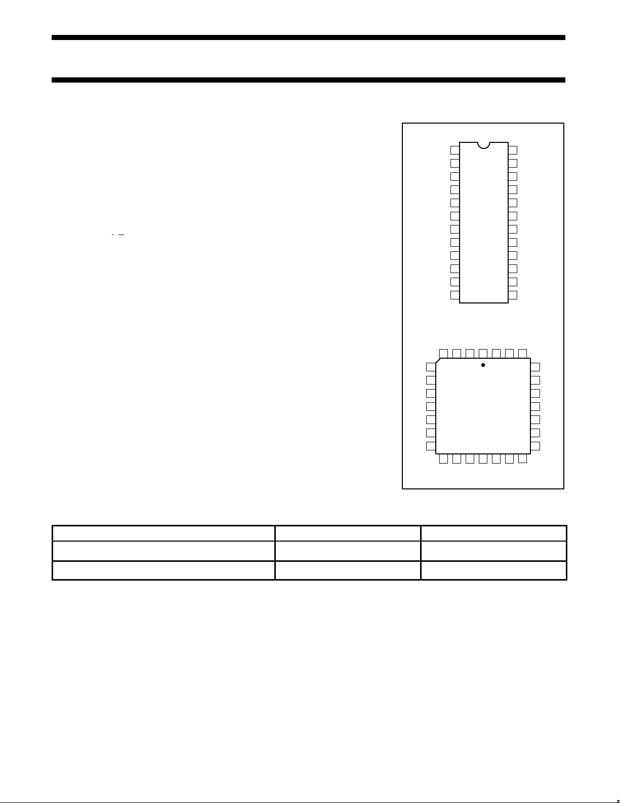
PIN CONFIGURATIONS
1234
5
6
7
8
9
10
11
12 13 14 15 16 17
18
19
20
21
22
23
24
25
262728
1
2
3
4
5
6
7
8
9
10
11
12 13
14
15
16
17
18
19
20
21
22
23
24
N Package
I0
I1
I2
I3
I4
I5
I6
I7
I8
I9
I10
V
CC
B9
B8
B7
B6
B5
B4
B3
B2
B1
B0
I11
GND
A Package
N = Plastic DIP (300mil-wide)
I0I1I2I3
V
CC
B9 B8
NC
I4
I5
I6
I7
I8
NC
I9 I10
GND
I11 B0 B1 B2
NC
B3
B7
B6
B5
B4
NC
A = Plastic Leaded Chip Carrier
ORDERING INFORMATION
DESCRIPTION ORDER CODE DRAWING NUMBER
24-Pin Plastic Dual-In-Line 300mil-wide PLS173N 0410D
28-Pin Plastic Leaded Chip Carrier PLS173A 0401F

Philips Semiconductors Programmable Logic Devices Product specification
PLS173
Programmable logic array
(22 × 42 × 10)
October 22, 1993
26
LOGIC DIAGRAM
NOTES:
1. All programmed ‘AND’ gate locations are pulled to logic “1”.
2. All programmed ‘OR’ gate locations are pulled to logic “0”.
3. Programmable connection.
(LOGIC TERMS–P) (CONTROL TERMS)
1
2
3
4
5
6
7
8
9
10
11
13
14
15
16
17
18
19
20
21
22
23
I0
I1
I2
I3
I4
I5
I6
I7
I8
I9
I10
I11
B9
B8
B7
B6
B5
B4
B3
B2
B1
B0
31 24 23 16 15 8 7 0
D
9D8D7D6D5D4D3D2D1D0
S
9
S
8
S
7
S
6
S
5
S
4
S
3
S
2
S
1
S
0
X
9
X
8
X
7
X
6
X
5
X
4
X
3
X
2
X
1
X
0
B9
B8
B7
B6
B5
B4
B3
B2
B1
B0

TYPICAL PRODUCT TERM:
Pn = A ⋅ B
⋅ C ⋅ D ⋅ . . .
TYPICAL LOGIC FUNCTION:
AT OUTPUT POLARITY = H
Z = P0 + P1 + P2 . . .
AT OUTPUT POLARITY + L
Z = P0 + P1 + P2 +
. . .
Z = P0
⋅ P1 ⋅ P2 ⋅ . . .
NOTES:
1. For each of the 10 outputs, either function Z
(Active-High) or Z
(Active-Low) is available, but not
both. The desired output polarity is programmed
via the EX-OR gates.
2. ZX, A, B, C, etc. are user defined connections to
fixed inputs (I), and bidirectional pins (B).
TEMPERATURE
Maximum junction 150°C
Maximum ambient 75
°C
Allowable thermal rise 75
°C
ambient to junction
The PLS173 is also processed to military
requirements for operation over the military
temperature range. For specifications and
ordering information, consult the Philips
Semiconductors Military Data Handbook.
Philips Semiconductors Programmable Logic Devices Product specification
PLS173
Programmable logic array
(22 × 42 × 10)
October 22, 1993
27
FUNCTIONAL DIAGRAM LOGIC FUNCTION
P
31
P
0
D
0
D
9
I0
I11
B0
B9
B9
B0
S
0
S
9
X
9
X
0
ABSOLUTE MAXIMUM RATINGS
1
THERMAL RATINGS
RATING
SYMBOL PARAMETER Min Max UNIT
V
CC
Supply voltage +7 V
DC
V
IN
Input voltage +5.5 V
DC
V
OUT
Output voltage +5.5 V
DC
I
IN
Input currents –30 +30 mA
I
OUT
Output currents +100 mA
T
amb
Operating free-air temperature range 0 +75 °C
T
stg
Storage temperature range –65 +150 °C
NOTES:
1. Stresses above those listed may cause malfunction or permanent damage to the device. This
is a stress rating only. Functional operation at these or any other condition above those
indicated in the operational and programming specification of the device is not implied.
 Loading...