

Philips PLS153A, PLS153AN, PLS153N Datasheet
Philips Semiconductors Programmable Logic Devices Product specification
PLS153/A
Programmable logic arrays
(18 × 42 × 10)
1
October 22, 1993 853–0311 11164
DESCRIPTION
The PLS153 and PLS153A are two-level
logic elements, consisting of 42 AND gates
and 10 OR gates with fusible link connections
for programming I/O polarity and direction.
All AND gates are linked to 8 inputs (I) and
10 bidirectional I/O lines (B). These yield
variable I/O gate configurations via 10
direction control gates (D), ranging from 18
inputs to 10 outputs.
On-chip T/C buffers couple either True (I, B)
or Complement (I
, B) input polarities to all
AND gates, whose outputs can be optionally
linked to all OR gates. Their output polarity, in
turn, is individually programmable through a
set of EX-OR gates for implementing
AND/OR or AND/NOR logic functions.
The PLS153 and PLS153A are
field-programmable, enabling the user to
quickly generate custom patterns using
standard programming equipment.
FEATURES
•Field-Programmable (Ni-Cr links)
•8 inputs
•42 AND gates
•10 OR gates
•10 bidirectional I/O lines
•Active-High or -Low outputs
•42 product terms:
– 32 logic terms
– 10 control terms
•I/O propagation delay:
– PLS153: 40ns (max)
– PLS153A: 30ns (max)
•Input loading: –100µA (max)
•Power dissipation: 650mW (typ)
•3-State outputs
•TTL compatible
APPLICATIONS
•Random logic
•Code converters
•Fault detectors
•Function generators
•Address mapping
•Multiplexing
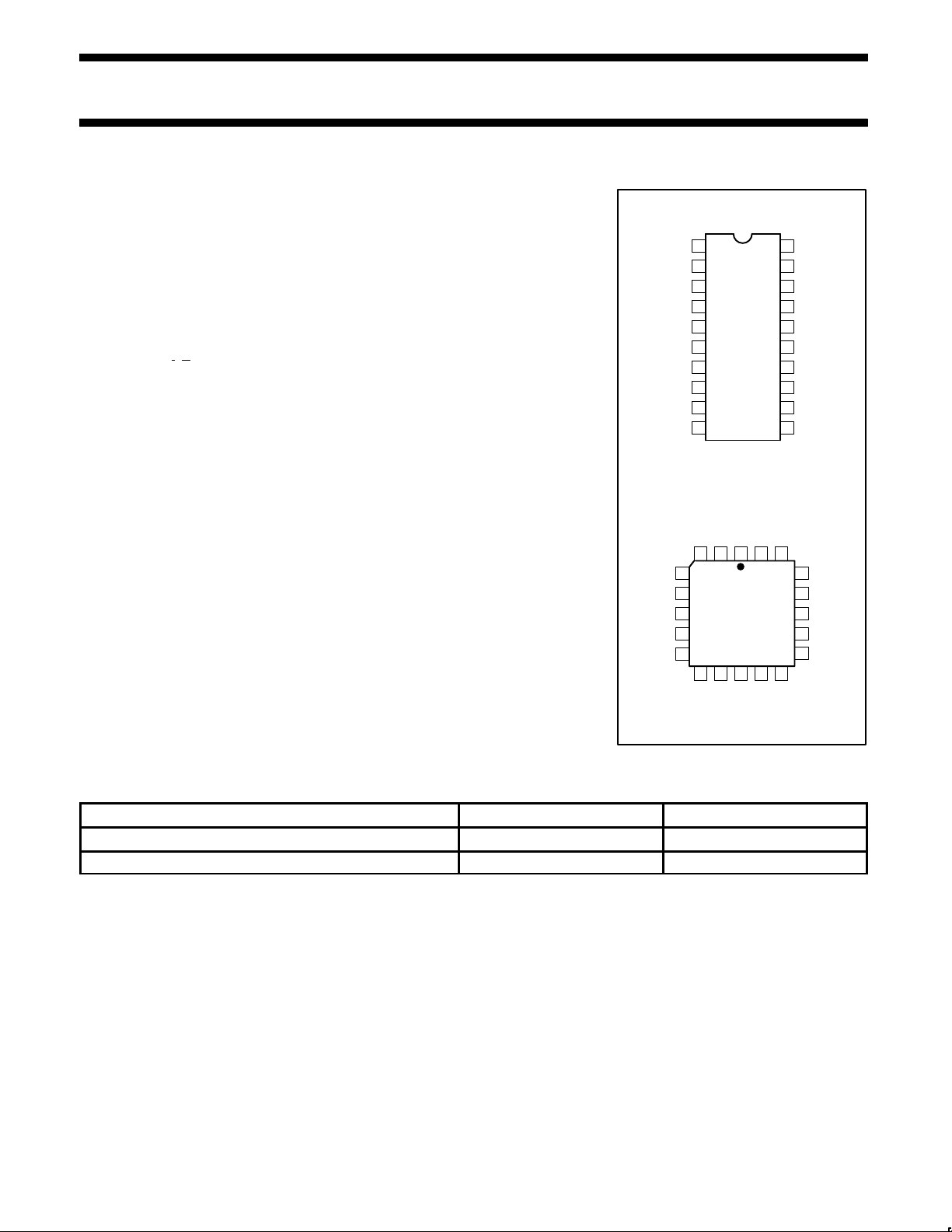
PIN CONFIGURATIONS
1
2
3
4
5
6
7
8
9
10 11
12
13
14
15
16
17
18
19
20
N Package
I
0
I
1
I
2
I
3
I
4
I
5
I
6
I
7
B
0
B
2
GND
B
3
B
4
B
5
B
6
B
7
B
8
B
9
V
CC
B
1
123
4
5
6
7
8
9 10 11 12 13
14
15
16
17
18
1920
A Package
N = Plastic DIP (300mil-wide)
A = Plastic Leaded Chip Carrier
B
2B3
B
4
B
5
B
6
B
7
B
8
B9V
CC
B
1
I0I1I
2
I
3
I
4
I
5
I
6
I
7
B
0
GND
SP00274
ORDERING INFORMATION
DESCRIPTION ORDER CODE DRAWING NUMBER
20-Pin Plastic Dual In-Line, 300mil-wide PLS153N, PLS153AN 0408B
20-Pin Plastic Leaded Chip Carrier PLS153A, PLS153AA 0400E

Philips Semiconductors Programmable Logic Devices Product specification
PLS153/A
Programmable logic arrays
(18 × 42 × 10)
October 22, 1993
2
LOGIC DIAGRAM
NOTES:
1. All programmed ‘AND’ gate locations are pulled to logic “1”.
2. All programmed ‘OR’ gate locations are pulled to logic “0”.
3. Programmable connection.
(LOGIC TERMS–P) (CONTROL TERMS)
1
2
3
4
5
6
7
8
9
11
12
13
14
15
16
17
18
19
I0
I1
I2
I3
I4
I5
I6
I7
B9
B8
B7
B6
B5
B4
B3
B2
B1
B0
31 24 23 16 15 8 7 0
D9D8D7D6D5D4D3D2D1D
0
S
9
S
8
S
7
S
6
S
5
S
4
S
3
S
2
S
1
S
0
X
9
X
8
X
7
X
6
X
5
X
4
X
3
X
2
X
1
X
0
B9
B8
B7
B6
B5
B4
B3
B2
B1
B0
SP00276

Philips Semiconductors Programmable Logic Devices Product specification
PLS153/A
Programmable logic arrays
(18 × 42 × 10)
October 22, 1993
3
FUNCTIONAL DIAGRAM
P
31
P
0
D
0
D
9
I
0
I
7
B
0
B
9
B
9
B
0
S
0
S
9
X
9
X
0
SP00277
ABSOLUTE MAXIMUM RA TINGS
1
RATINGS
SYMBOL PARAMETER MIN MAX UNIT
V
CC
Supply voltage +7 V
DC
V
IN
Input voltage +5.5 V
DC
V
OUT
Output voltage +5.5 V
DC
I
IN
Input currents –30 +30 mA
I
OUT
Output currents +100 mA
T
amb
Operating temperature range 0 +75 °C
T
stg
Storage temperature range –65 +150 °C
NOTES:
1. Stresses above those listed may cause malfunction or permanent damage to the device. This
is a stress rating only. Functional operation at these or any other condition above those
indicated in the operational and programming specification of the device is not implied.
 Loading...