

Philips PCK2057DGG Datasheet
INTEGRATED CIRCUITS
PCK2057
2
70 – 190 MHz I
C differential
1:10 clock driver
Product data
Supersedes data of 2001 May 09
File under Integrated Circuits, ICL03
2001 Jun 12
Philips Semiconductors Product data
2
70 – 190 MHz I
C differential 1:10 clock driver
PCK2057
FEA TURES
•Optimized for clock distribution in DDR (Double Data Rate)
SDRAM applications supporting DDR 200/266/300/333
•Full DDR solution provided when used with PCK2002P or
PCK2002PL, and PCK2022RA
•1-to-10 differential clock distribution
•Very low jitter (< 100 ps)
•Operation from 2.2 V to 2.7 V AV
and 2.3 V to 2.7 V V
DD
DD
•SSTL_2 interface clock inputs and outputs
•HCSL to SSTL_2 input conversion
•Test mode enables buffers while disabling PLL
•Tolerant of Spread Spectrum input clock
•3.3 V I
•2.5 V I
2
C support with 3.3 V VDDI2C
2
C support with 2.5 V VDDI2C
•Form, fit, and function compatible with CDCV850
DESCRIPTION
The PCK2057 is a high-performance, low-skew, low-jitter zero delay
is tied to
DD
) to ten
buffer that distributes a differential clock input pair (CLK, CLK
differential pairs of clock outputs and one differential pair of
feedback clock outputs. The clock outputs are controlled by the
clock inputs (CLK, CLK
), the feedback clocks (FBIN, FBIN), the
2-line serial interface (SDA, SCL), and the analog power input
(AV
). The two-line serial interface (I2C) can put the individual
DD
output clock pairs in a high-impedance state. When AV
GND, the PLL is turned off and bypassed for test purposes.
The device provides a standard mode (100 kbits) I
2
C interface for
device control. The implementation is as a slave/receiver. The serial
inputs (SDA, SCL) provide integrated pull-up resistors (typically
100 kΩ).
Two 8-bit, 2-line serial registers provide individual enable control for
each output pair. All outputs default to enabled at power-up. Each
output pair can be placed in a high-impedance mode, when a
low-level control bit is written to the control register. The registers
must be accessed in sequential order (i.e., random access of the
registers is not supported). The I
with either 2.5 V or 3.3 V (V
2
C interface circuit can be supplied
I2C).
DD
Since the PCK2057 is based on PLL circuitry, it requires a
stabilization time to achieve phase-lock of the PLL. This stabilization
time is required following power-up.
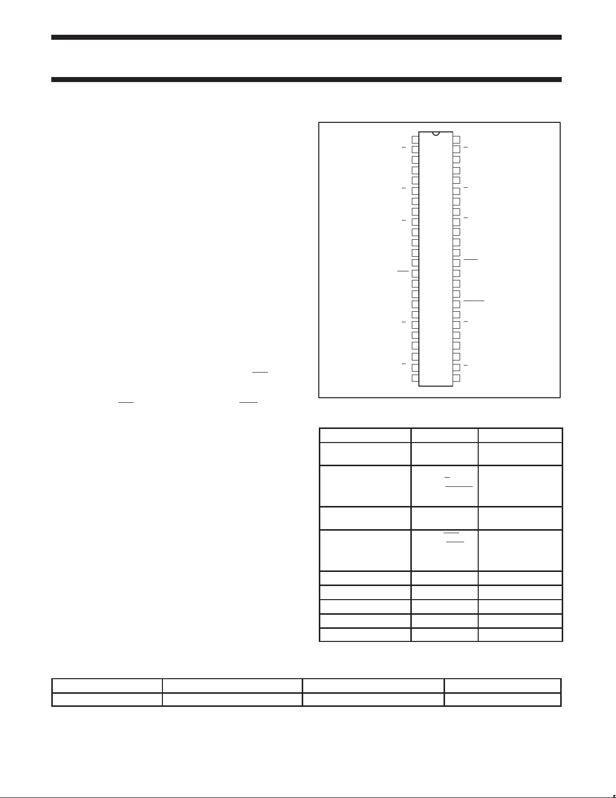
PIN CONFIGURATION
1
GND
Y
2
0
Y
3
0
4
V
DDQ
Y
5
1
Y
6
1
GND
7
8
GND
9
Y
2
Y
10
2
V
11
DDQ
SCL
12
13
CLK
14
CLK
VDDI2C
15
AV
16
DD
17
AGND
GND
18
Y
19
3
Y
20
3
21
V
DDQ
Y
22
4
Y
4
23
24
GND
PIN DESCRIPTION
PINS SYMBOL DESCRIPTION
1, 7, 8, 18, 24, 25, 31,
41, 42, 48
2, 3, 5, 6, 9, 10, 19, 20,
22, 23, 26, 27, 29, 30,
32, 33, 39, 40, 43, 44,
46, 47
4, 11, 21, 28, 34, 38,
45
13, 14, 35, 36 CLK, CLK,
16 AV
17 AGND Analog ground
37 SDA Serial data
12 SCL Serial clock
15 VDDI2C I2C power
FBOUT, FBOUT
48
GND
47
Y
5
Y
46
5
45
V
DDQ
Y
44
6
Y
6
43
GND
42
GND
41
Y
7
40
Y
39
7
V
DDQ
38
SDA
37
FBIN
36
FBIN
35
V
34
DDQ
FBOUT
33
FBOUT
32
GND
31
Y
8
30
Y
29
8
V
28
DDQ
Y
9
27
26
Y
9
GND
25
SW00506
GND Ground
Yn, Yn,
V
DDQ
FBIN, FBIN
DD
Buffered output
copies of input clock,
CLK
2.5 V supply
Differential clock
inputs and feedback
differential clock
inputs
Analog power
ORDERING INFORMATION
PACKAGES TEMPERATURE RANGE ORDER CODE DRAWING NUMBER
48-Pin Plastic TSSOP 0 to +70 °C PCK2057DGG SOT362-1
2001 Jun 12 853–2253 26485
2
Philips Semiconductors Product data
2
70 – 190 MHz I
C differential 1:10 clock driver
PCK2057
FUNCTION TABLE
1
AV
DD
INPUTS OUTPUTS
CLK CLK Y Y FBOUT FBOUT
GND L H L H L H Bypassed/OFF
GND H L H L H L Bypassed/OFF
2.5 V (nom.) L H L H L H ON
2.5 V (nom.) H L H L H L ON
NOTES:
H = HIGH voltage level
L = LOW voltage level
1. Each output pair (except FBOUT and FBOUT
) can be put into a high-impedance state through the 2-line serial interface.
PLL ON/OFF
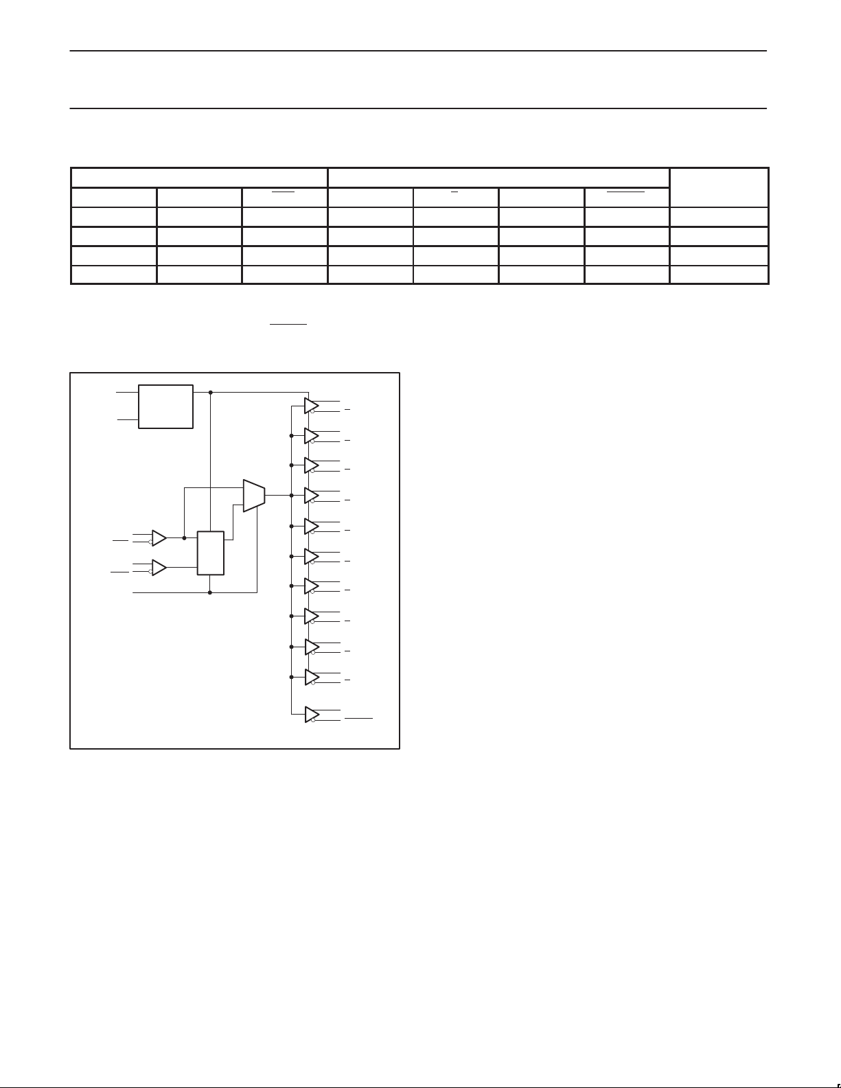
BLOCK DIAGRAM
SDA
SCL
CLK
CLK
FBIN
FBIN
AV
DD
CONTROL
LOGIC
PLL
Y
0
Y
0
Y
1
Y
1
Y
2
Y
2
Y
3
Y
3
Y
4
Y
4
Y
5
Y
5
Y
6
Y
6
Y
7
Y
7
Y
8
Y
8
Y
9
Y
9
FBOUT
FBOUT
SW00507
2001 Jun 12
3

Philips Semiconductors Product data
2
70 – 190 MHz I
C differential 1:10 clock driver
PCK2057
I2C ADDRESS
11 0 1001
R/W
su01394
I2C CONSIDERA TIONS
I2C has been chosen as the serial bus interface to control the PCK2057. I2C was chosen to support the JEDEC proposal JC-42.5 168 Pin
Unbuffered SDRAM DIMM. All vendors are required to determine the legal issues associated with the manufacture of I
1) Address assignment: The clock driver in this specification uses the single, 7-bit address shown below. All devices can use the address if only
one master clock driver is used in a design. The address can be re-used for the CKBF device if no other conflicting I
the system.
The following address was confirmed by Philips on 09/04/96.
A6 A5 A4 A3 A2 A1 A0 R/W
11010010
NOTE: The R/W
bit is used by the I2C controller as a data direction bit. A ‘zero’ indicates a transmission (WRITE) to the clock device. A ‘one’
indicates a request for data (READ) from the clock driver. Since the definition of the clock buffer only allows the controller to WRITE data; the
bit of the address will always be seen as ‘zero’. Optimal address decoding of this bit is left to the vendor.
R/W
2) Data Transfer Rate: 100 kbits/s (standard mode) is the base functionality required. Fast mode (400 kbits/s) functionality is optional.
3) Logic Levels: I
2
C logic levels are based on a percentage of VDD for the controller and other devices on the bus. Assume all devices are
based on a 3.3 Volt supply.
4) Data Byte Format: Byte format is 8 Bits as described in the following appendices.
2
5) Data Protocol: To simplify the clock I
C interface, the clock driver serial protocol was specified to use only block writes from the controller.
The bytes must be accessed in sequential order from lowest to highest byte with the ability to stop after any complete byte has been
transferred. Indexed bytes are not allowed. However, the SMBus controller has a more specific format than the generic I
The clock driver must meet this protocol which is more rigorous than previously stated I2C protocol. Treat the description from the viewpoint of
controller. The controller “writes” to the clock driver.
2
C devices.
2
C clock driver is used in
2
C protocol.
1 bit 7 bits 1 1 8 bits 1
Start bit Slave Address R/W DUMMY DUMMY
Ack Data Byte 1Ack Data Byte 2 Ack StopAckAck
1 bit 8 bits 1 18 bits 1
SW00911
NOTE: The acknowledgement bit is returned by the slave/receiver (the clock driver).
2
6) Electrical Characteristics: All electrical characteristics must meet the standard mode specifications found in section 15 of the I
C
specification.
a) Pull-Up Resistors: Any internal resistors pull-ups on the SDATA and SCLOCK inputs must be stated in the individual datasheet. The use of
internal pull-ups on these pins of below 100 kΩ is discouraged. Assume that the board designer will use a single external pull-up resistor for
each line and that these values are in the 5–6 kΩ range. Assume one I
clock driver plus one/two more I
2
C devices on the platform for capacitive loading purposes.
2
C device per DIMM (serial presence detect), one I2C controller, one
(b) Input Glitch Filters: Only fast mode I2C devices require input glitch filters to suppress bus noise. The clock driver is specified as a standard
mode device and is not required to support this feature.
For specific I
2001 Jun 12
2
C information, consult the Philips I2C Peripherals Data Handbook IC12 (1997).
4
 Loading...