

Philips PCK2023DGG, PCK2023DL Datasheet

INTEGRATED CIRCUITS
PCK2023
CK408 (66/100/133/200 MHz)
spread spectrum differential system
clock generator
Product data
File under Integrated Circuits — ICL03
2001 Sep 07
Philips Semiconductors Product data
CK408 (66/100/133/200 MHz) spread spectrum
differential system clock generator
FEA TURES
•3.3 V operation
•Three differential CPU clock pairs
•Ten PCI clocks at 3.3 V
•Six 66 MHz clocks at 3.3 V
•Two 48 MHz clocks at 3.3 V
•One 14.318 MHz reference clock
•66,100, 133 or 200 MHz operation
•Power management control pins
•CPU clock skew less than 200 ps cycle-to-cycle
•CPU clock skew less than 150 ps pin-to-pin
•1.5 ns to 3.5 ns delay on PCI pins
•Spread Spectrum capability
DESCRIPTION
The PCK2023 is a clock synthesizer/driver for a Pentium IV and
other similar processors.
The PCK2023 has three differential pair CPU current source
outputs. There are ten PCI clock outputs running at 33 MHz and two
48 MHz clocks. There are six 3V66 outputs. Finally, there is one
3.3 V reference clock at 14.318 MHz. All clock outputs meet Intel’s
drive strength, rise/fall times, jitter, accuracy, and skew
requirements.
The part possesses a dedicated power-down input pin for power
management control. This input is synchronized on-chip and
ensures glitch-free output transitions.
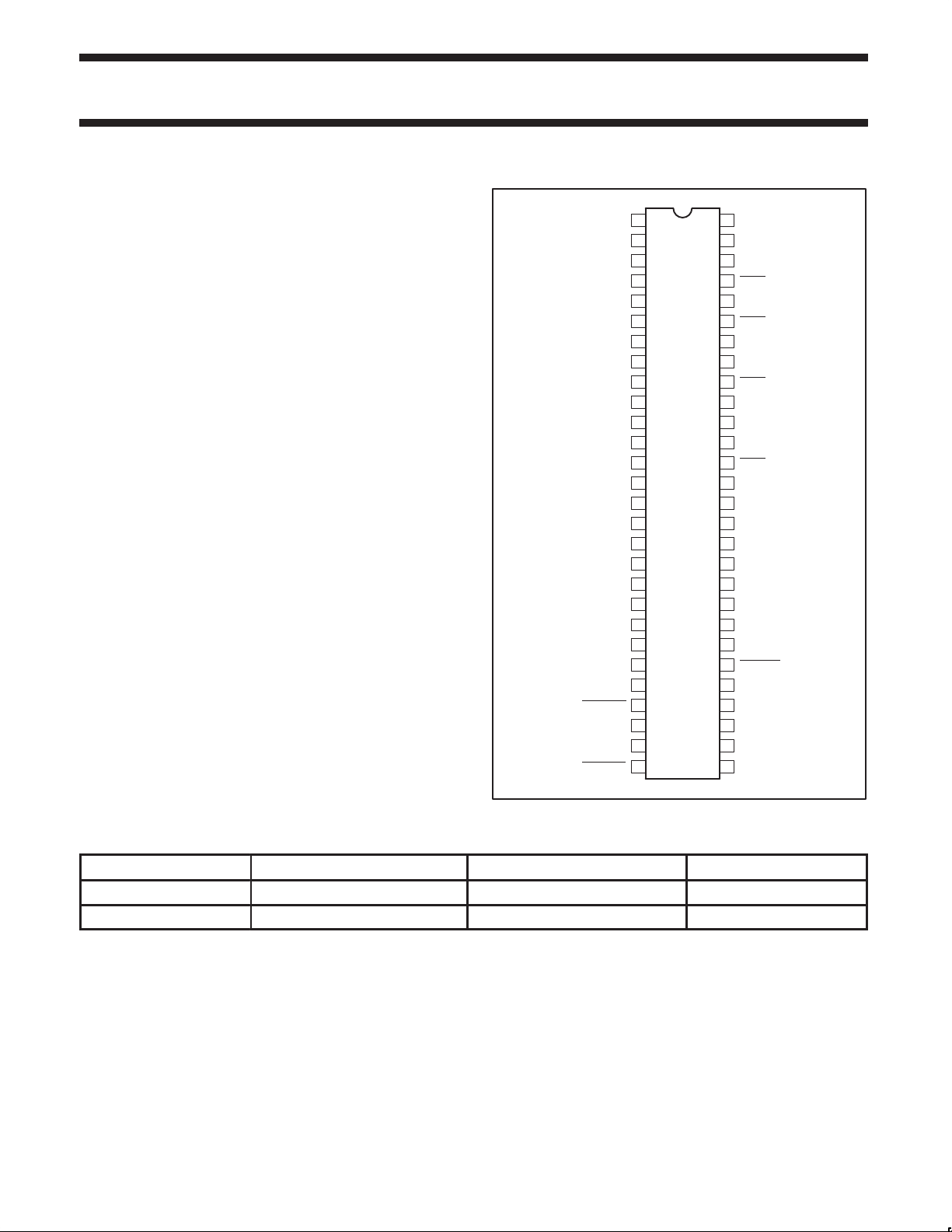
PIN CONFIGURATION
XTAL_In
XTAL_Out
V
PCIF0
PCIF1
PCIF2
V
V
PCI0
PCI1
V
V
PCI4
PCI5
PCI6
V
V
66Buff0/3V66_2
66Buff1/3V66_3
66Buff2/3V66_4
66In/3V66_5
PWRDWN
VDDA
1
DD
2
3
4
SS
5
6
7
8
DD
9
SS
10
11
12 45
13
14
DD
15
SS
16
17
18 39
19 38
DD
20
SS
21
22
23
24
25 32
26 31 V
27 30 SCLKVSSA
28 29Vtt_Pwrgd SDATA
PCK2023
REF_0
56V
S0
55
CPU3
54
CPU3
53
52
CPU0
51
CPU0
50
V
DD
CPU1
49
48
CPU1
47
V
SS
46
V
DD
CPU2PCI2
44PCI3
CPU2
Mult0
43
42
IREF
V
Iref
41
SS
40
S2
USB 48 MHz
DOT 48 MHz
37
48 MHz
V
DD
36
V
48 MHz
SS
35
3V66_1/VCH
34
PCI_Stop
33
3V66_0
V
DD
SS
SW00695
ORDERING INFORMATION
PACKAGES TEMPERATURE RANGE ORDER CODE DRAWING NUMBER
56-Pin Plastic SSOP 0 to +70 °C PCK2023DL SOT371-1
56-Pin Plastic TSSOP 0 to +70 °C PCK2023DGG SOT364-1
Intel and Pentium are registered trademarks of Intel Corporation.
2001 Sep 07 853-2278 27052
2

Philips Semiconductors Product data
CK408 (66/100/133/200 MHz) spread
spectrum differential system clock generator
PIN DESCRIPTION
PIN NUMBER SYMBOL FUNCTION
56 ref 3.3 V 14.318 MHz clock output.
2 XTAL_In 14.318 MHz crystal input.
3 XTAL_Out 14.318 MHz crystal output.
44, 45, 48, 49, 51, 52
33 3V66_0 3.3 V 66 MHz clock output.
35 3V66_1/VCH 3.3 V selectable through I2C to be 66 MHz or 48 MHz
24 66In/3V66_5 66 MHz input to buffered 66Buff and PCI or 66 MHz clock from internal VCO.
21, 22, 23 66Buff [2:0] / 3V66 [4:2] 66 MHz buffered outputs from 66 input or 66 MHz clocks from internal VCO.
5, 6, 7
10, 11, 12, 13, 16, 17,
18
39 USB Fixed 48 MHz clock output.
38 DOT Fixed 48 MHz clock output.
40 S2 Special 3.3 V 3 level input for mode selection.
54, 55 S1, S0 3.3 V LVTTL inputs for CPU frequency selection.
42 I
43 Mult0 3.3 V LVTTL input for selecting the current multiplier for the CPU outputs.
25 PWRDWN 3.3 V L VTTL input for PowerDown active low.
34 PCI_Stop 3.3 V LVTTL input for PCI_Stop active low.
53 CPU_Stop 3.3 V L VTTL input for CPU_Stop active low.
28 Vtt_Pwrgd
29 SDATA I2C compatible SDATA.
30 SCLOCK I2C compatible SCLOCK.
1, 8, 14, 19, 32, 37, 46,
50
26 VDDA 3.3 V power supply for PLL.
4, 9, 15, 20, 31, 36, 41,
47
27 VSSA Ground for PLL.
CPU & CPU
[2:0]
PCIF
[2:0]
PCI
[6:0]
ref
V
DD
V
SS
Differential CPU clock outputs.
33 MHz clocks divided down from 66 input or divided down from 3V66.
PCI clock outputs divided down from 66 input or divided down from 3V66.
A precision resistor is attached to this pin which is connected to the internal current
reference.
3.3 V LVTTL input is a level sensitive strobe used to determine when S [2:0] and Mult0
inputs are valid and ok to be sampled (active low).
3.3 V power supply for outputs.
Ground for outputs.
PCK2023
2001 Sep 07
3
Philips Semiconductors Product data
CK408 (66/100/133/200 MHz) spread
spectrum differential system clock generator
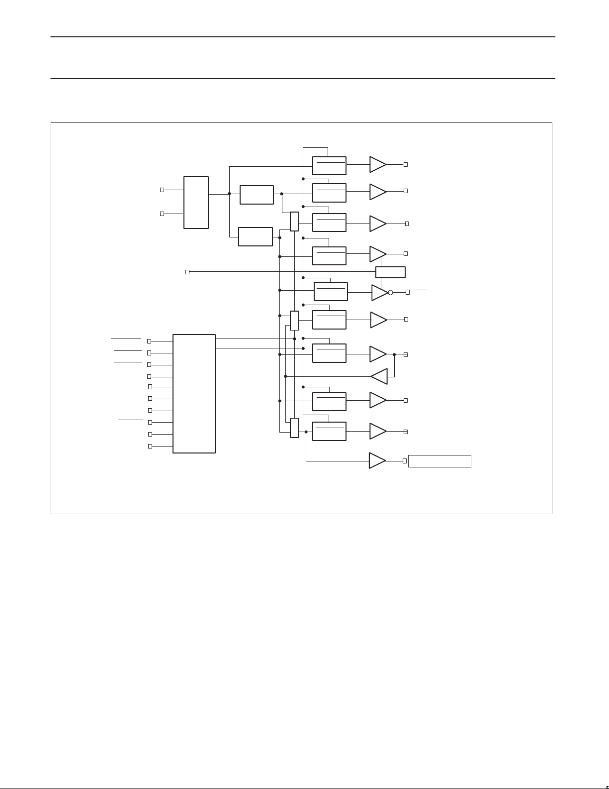
BLOCK DIAGRAM
XIN
XOUT
X
14.318
MHZ
IREF
OSC
X
X
USBPLL
SYSPLL
PWRDWN
PWRDWN
PWRDWN
PWRDWN
PWRDWN
PWRDWN
IBIAS
REF [0](14.318 MHz)
X
X
DOT/USB 48 MHz
3V66_1/VCH(48/66 MHz)
X
CPU [0–2](100/133 MHz)
X
CPU [0–2](100/133 MHz)
X
3V66 [2–4] (66 MHz)
X
PCK2023
CPU STOP
PCI STOP
PWRDWN
MULT0
Pwrgd
V
tt
SDA
SCL
X
X
X
S2
X
S1
X
S0
X
X
X
X
X
LOGIC
PWRDWN
PWRDWN
PWRDWN
66ln/3V66_5(66 MHz)
X
3V66_0 (66 MHz)
X
PCI [0–6](33 MHz)
X
PCIF [0–2] (33 MHz)
X
SW00861
2001 Sep 07
4

Philips Semiconductors Product data
CK408 (66/100/133/200 MHz) spread
PCK2023
spectrum differential system clock generator
FREQUENCY SELECT/FUNCTION TABLE
S2 S1 S0 CPU 3V66
66BUFF/
3V66
1 0 0 66 MHz 66 MHz 66 In 66 input 66 In/2 14.318 MHz 48 MHz 66/48 MHz
1 0 1 100 MHz 66 MHz 66 In 66 input 66 In/2 14.318 MHz 48 MHz 66/48 MHz
1 1 0 200 MHz 66 MHz 66 In 66 input 66 In/2 14.318 MHz 48 MHz 66/48 MHz
1 1 1 133 MHz 66 MHz 66 In 66 input 66 In/2 14.318 MHz 48 MHz 66/48 MHz
0 0 0 66 MHz 66 MHz 66 MHz 66 MHz 33 MHz 14.318 MHz 48 MHz 66/48 MHz
0 0 1 100 MHz 66 MHz 66 MHz 66 MHz 33 MHz 14.318 MHz 48 MHz 66/48 MHz
0 1 0 200 MHz 66 MHz 66 MHz 66 MHz 33 MHz 14.318 MHz 48 MHz 66/48 MHz
0 1 1 133 MHz 66 MHz 66 MHz 66 MHz 33 MHz 14.318 MHz 48 MHz 66/48 MHz
Mid 0 0 Low Hi Z Hi Z Hi Z Hi Z Hi Z Hi Z Hi-Z
Mid 0 1 Tclk/2 Tclk/4 Tclk/4 Tclk/4 Tclk/8 Tclk Tclk/2 Tclk/4
NOTE:
1. Mid is defined as a voltage level between 1.0 V and 1.8 V for 3 level input functionality. Low is below 0.8 V. High is above 2.0 V.
2. 3V66_1/VCH output frequency is set by the I
2
C.
3. Frequency of the 48 MHz outputs must be +167 ppm to match USB default.
4. Rref output min = 14.316 MHz, nominal = 14.31818, max = 14.32 MHz.
5. Tclk is a test clock over-driven on the XTAL_In input during test mode.
66In/
3V66_5
PCIF/PCI REF 0 USB/DOT
3V66_1/
VCH
POWER DOWN MODE
PWRDWN CPU CPU 3V66
1 Normal Normal Normal Normal Normal Normal Normal Normal Normal
0 I
*2 Float Low Low Low Low Low Low Low
ref
HOST SWING SELECT FUNCTIONS – CK408
MULT 0
0 50 Ω R
1 50 Ω R
CONDITIONS CONFIGURATION LOAD MIN. MAX.
I
OUT
I
OUT
VDD = 3.3 V All combinations,
VDD = 3.3 V ±5% All combinations,
BOARD
IMPEDANCE
Nominal test load for given configuration –7% of I
see Table above
Nominal test load for given configuration –12% of I
see Table above
66BUFF/
I
= 221.1%
ref
I
= 5.00 mA
ref
= 475.1%
ref
I
= 2.32 mA
ref
3V66
ref
66In/
3V66_5
PCIF/PCI REF 0 USB/DOT
I
OH
IOH = 4*I
IOH = 6*I
ref
ref
See Table above
OH
See Table above
OH
VOH @ 50 W
1.0 V
0.7 V
See Table above
See Table above
+7% of I
+12% of I
3V66_1/
VCH
OH
OH
2001 Sep 07
5

Philips Semiconductors Product data
SYMBOL
PARAMETER
CONDITION
UNIT
SYMBOL
PARAMETER
CONDITIONS
UNIT
NOTES
CK408 (66/100/133/200 MHz) spread
PCK2023
spectrum differential system clock generator
ABSOLUTE MAXIMUM RATINGS
V
DD3
I
IK
V
I
I
OK
V
O
I
O
T
stg
P
tot
NOTES:
1. Stresses beyond those listed may cause permanent damage to the device. These are stress ratings only and functional operation of the
device at these or any other conditions beyond those indicated under “Recommended Operating Conditions” is not implied. Exposure to
absolute-maximum-rated conditions for extended periods may affect device reliability .
2. The input and output voltage ratings may be exceeded if the input and output current ratings are observed.
DC 3.3 V supply –0.5 +4.6 V
DC input diode current VI < 0 — –50 mA
DC input voltage Note 2 — — V
DC output diode current VO > VDD or VO < 0 — ±50 mA
DC output voltage Note 2 –0.5 VDD + 0.5 V
DC output source or sink current VO = 0 to V
Storage temperature range –65 +150 °C
Power dissipation per package
plastic medium-shrink (SSOP)
DC OPERA TING CONDITIONS
V
DD3
AV
V
IH
V
IL
V
OL3
V
OH3
I
IL
f
ref
C
IN
C
XTAL
C
OUT
L
PIN
T
amb
NOTES:
1. Input leakage current does not include inputs with pull up or pull down resistors.
2. This is a recommendation, not an absolute requirement.
3. As seen by the crystal. Device is intended to be used with a 17–20 pF AT crystal.
DC 3.3 V supply voltage 3.135 3.465 V
DC 3.3 V analog supply voltage 3.135 3.465 V
DD
3.3 V input high voltage 2.0 VDD + 0.3 V
3.3 V input high voltage VSS – 0.3 0.8 V
3.3 V input low voltage IOL = 1.0 mA — 0.4 V
3.3 V input high voltage IOH = 1.0 mA 2.4 — V
Input leakage current 0 < VIN < V
reference frequency , oscillator normal value 14.31818 14.31818 MHz
Input pin capacitance — 5 pF 2
Xtal pin capacitance 13.5 22.5 pF 3
Output pin capacitance — 6 pF 2
Pin inductance — 7 nH 2
Operating ambient temperature range in free
air
1, 2
DD
For temperature range: –40 to +125°C
above +55°C derate linearly with 11.3 mW/K
DD
LIMITS
MIN MAX
— ±50 mA
— 850 mW
LIMITS
MIN MAX
–5 +5 µA 1
0 +70 °C
2001 Sep 07
6
Philips Semiconductors Product data
TEST CONDITIONS
IOH48 MHz USB, VCH
y
mA
IOL48 MHz USB, VCH
y
mA
IOH48 MHz DOT
y
mA
IOL48 MHz DOT
y
mA
I
,, ,
y
mA
I
,, ,
y
mA
CK408 (66/100/133/200 MHz) spread
PCK2023
spectrum differential system clock generator
POWER MANAGEMENT
MAXIMUM 3.3 V SUPPLY CONSUMPTION
CONDITION
Power-down mode (PWRDWN = 0) 25 mA @ I
MAXIMUM DISCRETE CAP LOADS, V
ALL STATIC INPUTS = V
46 mA @ I
= 2.32 mA
ref
= 5.0 mA
ref
DD3
Full active 280 mA
CPU STOP FUNCTIONALITY
CPU_STOP CPU CPU 3V66 66BUFF PCIF/PCI USB/DOT
1 Normal Normal 66 MHz 66 input 66 input/2 48 MHz
0 I
*2 Float 66 MHz 66 input 66 input/2 48 MHz
ref
DC CHARACTERISTICS
SYMBOL PARAMETER
VDD (V) OTHER MIN TYP MAX
3.135 V
3.465 V
3.135 V
3.465 V
3.135 V
3.465 V
3.135 V
3.465 V
REF, PCI, PCIF,
OH
3V66, 66BUFF
REF, PCI, PCIF,
OL
3V66, 66BUFF
V
±I
CPU/CPU VSS = 0.0
OL
±I
Input leakage current 3.365 0 < VIN < V
I
3-State output OFF-State
OZ
current
3.135 V
3.465 V
3.135 V
3.465 V
3.465
NOTE:
1. All clock outputs loaded with maximum lump capacitance test load specified in AC characteristics section.
= 1.0 V
OUT
= 3.135 V
OUT
= 1.95 V
OUT
= 0.4 V
OUT
= 1.0 V
OUT
= 3.135 V
OUT
= 1.95 V
OUT
= 0.4 V
OUT
= 1.0 V
OUT
= 3.135 V
OUT
= 1.95 V
OUT
= 0.4 V
OUT
RS = 33.2 Ω
RP= 49.9 Ω
V
=
OUT
V
or GND
DD
DD3
Type 3A
12–60 Ω
Type 3A
12–60 Ω
Type 3B
12–60 Ω
Type 3B
12–60 Ω
Type 5
12–55 Ω
Type 5
12–55 Ω
–29 — —
— — –23
29 — —
— — 27
–29 — —
— — –23
29 — —
— — 27
–33 — —
— — –33
30 — —
— — 38
Type X1 0.0 — 0.05 V
— –5 — 5 µA
IO = 0 — — 10 µA
= 3.465 V
DDL
OR V
SS
LIMITS
T
= 0 to +70 °C UNIT
amb
2001 Sep 07
7
Philips Semiconductors Product data
CK408 (66/100/133/200 MHz) spread
spectrum differential system clock generator
AC CHARACTERISTICS
V
= 3.3 V –5%; f
DD3
3V66 66 MHz TIMING REQUIREMENTS
SYMBOL PARAMETER
T
PERIOD
t
HIGH
t
LOW
t
RISE
t
FALL
t
JITTER
Edge rate rising edge rate 1.0 4.0 V/ns 12
Edge rate falling edge rate 1.0 4.0 V/ns 12
t
SKEW
t
SKEW
t
SKEW
= 14.31818 MHz
crystal
LIMITS
T
= 0 to +70 °C
amb
UNIT NOTES
MIN MAX
period 15.0 15.3 ns 8, 13
HIGH time 4.95 N/A ns 9
LOW time 4.55 N/A ns 10
rise time 0.5 2.0 ns 12
fall time 0.5 2.0 ns 12
cycle-to-cycle jitter — 250 ps
pin-to-pin skew 3V66 [1:0] 0.0 250 ps
pin-to-pin skew 3V66 [5:2] 0.0 250 ps
pin-to-pin skew 3V66 [5:0] 0.0 450 ps
PCK2023
66 MHz BUFFERED TIMING REQUIREMENTS
LIMITS
T
= 0 to +70 °C
SYMBOL PARAMETER
amb
UNITS NOTES
MIN MAX
t
RISE
t
FALL
t
PD
propagation delay from 66In to 66BUFF [2:0] 2.5 4.5 ns
rise time 0.5 2.0 ns 12
fall time 0.5 2.0 ns 12
Edge rate rising edge rate 1.0 4.0 V/ns 12
Edge rate falling edge rate 1.0 4.0 V/ns 12
t
SKEW
66 MHz buffered pin-to-pin skew 0.0 175 ps
PCIF/PCI AC TIMING REQUIREMENTS
LIMITS
T
= 0 to +70 °C
SYMBOL PARAMETER
T
PERIOD
t
HIGH
t
LOW
t
RISE
t
FALL
t
JITTER
period 30.0 N/A ns 8, 13
HIGH time 12.0 N/A ns 9
LOW time 12.0 N/A ns 10
rise time 0.5 2.0 ns 12
fall time 0.5 2.0 ns 12
cycle-to-cycle jitter — — ps
Edge rate rising edge rate 1.0 4.0 V/ns 12
Edge rate falling edge rate 1.0 4.0 V/ns 12
t
SKEW
t
PCI
pin-to-pin skew 0.0 500 ps
3V66 [5:0] leads 33 MHz PCI 1.5 3.5 ns
amb
MIN MAX
UNITS NOTES
2001 Sep 07
8
Philips Semiconductors Product data
CK408 (66/100/133/200 MHz) spread
spectrum differential system clock generator
USB 48 MHz AC TIMING REQUIREMENTS
SYMBOL PARAMETER
T
DOT 48 MHz AC TIMING REQUIREMENTS
T
(average) period nominal = 20.829 ns
PERIOD
t
HIGH
t
LOW
HIGH time 8.094 10.036 ns
LOW time 7.694 9.836 ns
f frequency 48.000 48.008 MHz 8
t
RISE
t
FALL
t
JITTER
rise time 1.0 2.0 ns 12
fall time 1.0 2.0 ns 12
cycle-to-cycle jitter 0 350 ps
Edge rate rising edge rate 1.0 2.0 V/ns
Edge rate falling edge rate 1.0 2.0 V/ns
SYMBOL PARAMETER
(average) period nominal = 20.829 ns
PERIOD
t
HIGH
t
LOW
HIGH time 8.094 10.036 ns
LOW time 7.694 9.836 ns
f frequency 48.000 48.008 MHz 8
t
RISE
t
FALL
t
JITTER
rise time 0.5 1.0 ns 12
fall time 0.5 1.0 ns 12
cycle-to-cycle jitter — 350 ps
Edge rate rising edge rate 2.0 4.0 V/ns
Edge rate falling edge rate 2.0 4.0 V/ns
t
SKEW
USB to DOT — 1000 ps
LIMITS
T
= 0 to +70 °C
amb
MIN MAX
LIMITS
T
= 0 to +70 °C
amb
MIN MAX
PCK2023
UNITS NOTES
UNITS NOTES
2001 Sep 07
9
 Loading...