

Philips PCF8820U Datasheet
INTEGRATED CIRCUITS
DATA SH EET
PCF8820
67 × 101 Grey-scale/ECB colour
dot matrix LCD driver
Product specification
File under Integrated Circuits, IC12
2000 Dec 07

Philips Semiconductors Product specification
67 × 101Grey-scale/ECB colour dotmatrix
LCD driver
CONTENTS
1 FEATURES
2 APPLICATIONS
3 GENERAL DESCRIPTION
4 ORDERING INFORMATION
5 BLOCK DIAGRAM
6 PINNING
6.1 Pad configuration
6.2 Pad functions
6.2.1 Row driver outputs
6.2.2 Column driver outputs
6.2.3 Ground supply
6.2.4 Supply voltage
6.2.5 Voltage multiplier output
6.2.6 Voltage multiplier regulation input
6.2.7 Supply voltage of bias voltage generator
6.2.8 LCD intermediate bias voltages
6.2.9 Serial data input
6.2.10 Serial data output
6.2.11 Serial clock input
6.2.12 Slave address inputs
6.2.13 Oscillator signal input
6.2.14 External reset input
6.2.15 Test pads
7 FUNCTIONAL DESCRIPTION
7.1 Oscillator
7.2 I2C-bus interface controller
7.3 Input filters
7.4 Display Data RAM (DDRAM)
7.5 Timing generator
7.6 Address counter
7.7 Display address counter
7.8 Command decoder
7.9 Column driver outputs
7.10 Row driver outputs
7.11 Bias voltage generator
7.12 High voltage generator
7.13 Temperature compensation
7.14 Temperature sensor
7.15 LCD driver waveforms
7.16 DDRAM to display mapping
7.17 DDRAM addressing
7.18 I2C-bus interface
7.18.1 Bit transfer
7.18.2 START and STOP conditions
7.18.3 System configuration
7.18.4 Acknowledge
7.18.5 I2C-bus protocol
7.18.6 Command decoder
7.18.7 Display data byte
8 INSTRUCTIONS
8.1 Description of the bit functions
8.1.1 Power-down mode
8.1.2 Partial screen mode
8.1.3 Y-address of DDRAM
8.1.4 Bias system
8.1.5 High voltage generator configuration
8.1.6 Temperature read-out
8.1.7 V
8.1.8 Grey-scale register and grey-scale level
8.1.9 Direct drive mode
8.1.10 Frame frequency calibration
8.2 Reset and initialization
9 LIMITING VALUES
10 HANDLING
11 DC CHARACTERISTICS
12 TIMING
13 APPLICATION INFORMATION
13.1 Programming example for the PCF8820
13.2 Examples of effects on the display
13.3 High voltage generator
13.4 Application for COG
13.5 Typical system configuration
13.6 External supply of V
14 BONDING PAD INFORMATION
15 DEVICE PROTECTION CIRCUITS
16 TRAY INFORMATION
17 DATA SHEET STATUS
18 DEFINITIONS
19 DISCLAIMERS
20 BARE DIE DISCLAIMER
21 PURCHASE OF PHILIPS I2C COMPONENTS
control register
LCD
PCF8820
LCDIN
2000 Dec 07 2

Philips Semiconductors Product specification
67 × 101 Grey-scale/ECB colour dot matrix
LCD driver
1 FEATURES
• Single-chip LCD controller and driver for grey-scale/
Electrically Controlled Birefringence (ECB) colour
• 4 grey levels/colours (2-bit) definable from 64 levels
• 67 row and 101 column outputs
• Display data RAM 67 × 101 × 2-bit with linear RAM
addressing
• Partial screen mode with reduced current consumption
(8 rows at top or bottom of display)
• On-chip:
– Generation of LCD supply voltage (V
external supply also possible
– Configurable voltage multiplier factor of
8, 7, 6, 5, 4, 3 or 2; direct drive also possible
– Selectable linear temperature compensation
of V
LCDOUT
– Generation of intermediate LCD bias voltages
– Oscillator requires noexternal components; external
clock also possible.
• Temperature read-out
• Fast mode I2C-bus interface (400 kbits/s)
• Frame frequency calibration via software
• Software selectable bias configuration
• Compatible with 4-bit, 8-bit or 16-bit microcontrollers
• Multiplex rates of 1 : 67 or 1 : 8
• Logic supply voltage range from 2.5 to 5.5 V
(V
DD1
to V
SS1
)
• High voltage generator supply voltage range from
2.7 to 5.5 V (V
DD2
to V
SS1
and V
DD3
to V
• Bias voltage generator supply voltage range
(V
LCDIN
to V
SS1
):
– From 7 to 14.5 V at a multiplex rate of 1 : 67
– From 4.5 to 14.5 V in partial screen mode at a
multiplex rate of 1 : 8.
• Low power consumption, suitable for battery operated
systems
• Slim chip layout, suitable for chip-on-glass applications
LCDOUT
)
SS2
);
PCF8820
• Software selectable top and bottom row swap for
adapting driver to different glass-layouts
• CMOS compatible inputs
• Manufactured in silicon gate CMOS process.
2 APPLICATIONS
• Mobile telecommunication systems
• Battery powered equipment
• Point of sale terminals
• Instrumentation
• Automotive information systems.
3 GENERAL DESCRIPTION
The PCF8820 is a low power CMOS LCD row/column
driver,designed to drive grey-scale/ ECB colour dot matrix
graphic displays at a multiplex rate of 1 : 67. In the partial
screen mode, only 8 rows are driven at a multiplex rate of
1:8.
This chip provides all the necessary display functions,
including on-chip generation of the LCD supply voltage
and LCD bias voltages. Consequently, fewer external
components are required and the power consumption is
low.
The PCF8820 interfaces with most microcontrollers and
communicates via a two-line bidirectional bus (I2C-bus).
All inputs are CMOS compatible.
Remark: the waveform generation for ECB colour is
identical to that used for grey-scale.
4 ORDERING INFORMATION
PACKAGE
TYPE NUMBER
NAME DESCRIPTION VERSION
PCF8820U − chip with bumps in tray −
2000 Dec 07 3
Philips Semiconductors Product specification
67 × 101 Grey-scale/ECB colour dot matrix
LCD driver
5 BLOCK DIAGRAM
handbook, full pagewidth
V
LCDSENSE
V
SDA_OUT
V
LCDIN
LCDOUT
V
DD1
V
DD2
V
DD3
V
SS1
V
SS2
T1
T2
T3
T4
T5
T6
SCL
SDA_IN
RES
166 to 171
172
173 to 178
179 to 184
188 to 194
185 to 187
206 to 211
198 to 203
205
221
212
213
217
218
215, 216
195, 196
197
219
V5V4V3V
162 3 to 25, 232 to 222,
BIAS
VOLTAGE
GENERATOR
HIGH
VOLTAGE
GENERATOR
TEMPERATURE
SENSOR
INPUT
FILTERS
2
DATA LATCHES
DISPLAY DATA RAM
2
C-BUS
I
INTERFACE
CONTROLLER
204
SA0
C0 to C100
26 to 126165164163
COLUMN
DRIVERS
DISPLAY
(DDRAM)
214
SA1
R0 to R66
DRIVERS
COMMAND
DECODER
148 to 127, 151 to 161
ROW
PCF8820
OSCILLATOR
TIMING
GENERATOR
DISPLAY
ADDRESS
COUNTER
ADDRESS
COUNTER
PCF8820
220
MGT114
OSC
Fig.1 Block diagram.
2000 Dec 07 4

Philips Semiconductors Product specification
67 × 101 Grey-scale/ECB colour dot matrix
LCD driver
6 PINNING
6.1 Pad configuration
SYMBOL PAD DESCRIPTION
R0 to R22 3 to 25 LCD row driver outputs (block 1)
R23 to R33 232 to 222 LCD row driver outputs (block 2)
R34 to R55 148 to 127 LCD row driver outputs (block 3)
R56 to R66 151 to 161 LCD row driver outputs (block 4)
C0 to C100 26 to 126 LCD column driver outputs
V
SS1
V
SS2
V
DD1
V
DD2
V
DD3
V
LCDOUT
V
LCDSENSE
V
LCDIN
V
2
V
3
V
4
V
5
SDA_IN 195 and 196 serial data input
SDA_OUT 197 serial data output (acknowledge)
SCL 215 and 216 serial clock input
SA0 204 I
SA1 214 I
OSC 220 oscillator signal input
RES 219 external reset input (active LOW)
T1 205 test 1 input
T2 221 test 2 output
T3 212 test 3 I/O
T4 213 test 4 I/O
T5 217 test 5 input
T6 218 test 6 output
206 to 211 ground supply 1
198 to 203 ground supply 2
179 to 184 supply voltage 1 of logic
188 to 194 supply voltage 2 of high voltage generator; temperature read-out
185 to 187 supply voltage 3 of high voltage generator; temperature read-out
173 to 178 voltage multiplier output
172 voltage multiplier regulation input
166 to 171 supply voltage for LCD (bias voltage generator)
165 LCD intermediate bias voltage 2; for test purposes only
164 LCD intermediate bias voltage 3; for test purposes only
163 LCD intermediate bias voltage 4; for test purposes only
162 LCD intermediate bias voltage 5; for test purposes only
2
C-bus slave address input 0 (bit 0)
2
C-bus slave address input 1 (bit 1)
PCF8820
The pad configuration is shown in Fig.32.
2000 Dec 07 5

Philips Semiconductors Product specification
67 × 101 Grey-scale/ECB colour dot matrix
LCD driver
6.2 Pad functions
6.2.1 ROW DRIVER OUTPUTS
Rowdriveroutputs(R0 to R66)aretheoutputsforthe LCD
rowdrivesignals.Theyshouldbeconnecteddirectlytothe
67 rows of the LCD. If less than 67 rows are required, the
unused outputs must be left open-circuit.
6.2.2 COLUMN DRIVER OUTPUTS
Columndriver outputs (C0 to C100) are the outputs for the
LCD column drive signals. They should be connected
directly to the 101 columns of the LCD. If less than
101 columns are required, the unused column outputs
must be left open-circuit.
6.2.3 GROUND SUPPLY
The ground supply rails (V
connected together. V
V
is related to V
SS2
DD2
SS1
.
and V
SS1
SS2
is related to V
) must be
and V
DD1
DD3
;
PCF8820
When an external supply voltage is used, pads V
V
LCDSENSE
together. However, if pads V
both connected to pad V
and V
do not have to be connected
LCDOUT
LCDSENSE
, the current consumption
LCDIN
and V
LCDOUT
can be reduced under the following conditions:
• The output of V
is set to high-impedance
LCDOUT
(see Table 8)
• The HIGH voltage programming range is selected by
setting bit PRS = 1, the maximum voltage multiplier on
factor 8 and the V
control register on the maximum
LCD
value (see Table 2).
6.2.8 LCD INTERMEDIATE BIAS VOLTAGES
The LCD intermediate bias voltages (V2,V3,V4and V5)
which are applied to the LCD columns and rows are
present on these pads for test purposes. They must be left
open-circuit in the application.
6.2.9 SERIAL DATA INPUT
LCDIN
are
,
6.2.4 SUPPLY VOLTAGE
The supply voltage rails (V
DD1,VDD2
and V
) must be
DD3
connectedtogether when the same supply is used for both
the logic circuits and for the voltage multiplier. When the
circuits are fed separately, V
DD2
and V
DD3
must be
connected to the same supply.
6.2.5 VOLTAGE MULTIPLIER OUTPUT
V
is the output of the voltage multiplier of the high
LCDOUT
voltage generator.
6.2.6 VOLTAGE MULTIPLIER REGULATION INPUT
V
LCDSENSE
multiplier and must be connected to V
is the regulation input of the high voltage
.
LCDOUT
6.2.7 SUPPLY VOLTAGE OF BIAS VOLTAGE GENERATOR
V
is the supply voltage on pad V
LCD
LCDIN
for the bias
voltage generator which supplies the LCD outputs. The
voltage on pad V
If V
is generated internally, pad V
LCD
connected to pad V
If V
is supplied externally, the external supply voltage
LCD
must be connected to pad V
voltagemustbeappliedafterapplyingV
removed before or when removing V
must not be lower than V
LCDIN
.
LCDIN
. An external supply
LCDIN
must be
LCDOUT
,anditmustbe
DD1
(see Fig.25). It is
DD1
DD1
.
recommended that an external supply voltage is applied
after leaving the reset state. The external supply voltage
can stay applied in the Power-down mode.
SDA_IN is the serial data input from the I2C-bus.
6.2.10 SERIAL DATA OUTPUT
SDA_OUT is the serial data output (data, acknowledge)
for the I2C-bus. Connecting pad SDA_OUT to
pad SDA_IN makes the SDA line fully I2C-bus compatible.
Not connecting pad SDA_IN to pad SDA_OUT allows the
devicetobeusedin applications inwhichtheacknowledge
bitisnotrequired. In Chip-On-Glass (COG) applications, it
is sometimes beneficial not to connect pad SDA_OUT to
pad SDA_IN. This is because in COG applications where
the track resistance from pad SDA_OUT to the system
SDA line is significant, a voltage divider is created by the
bus pull-up resistor and the Indium Tin Oxide (ITO) track
resistance. This divider could prevent the PCF8820 from
asserting a valid logic 0 level during an acknowledge
cycle.
In COG applications, where the acknowledge cycle is
required, the track resistance from the pad SDA_OUT to
the system SDA line must be minimized to guarantee a
valid LOW-level.
6.2.11 SERIAL CLOCK INPUT
SCL is the serial clock input from the I2C-bus.
2000 Dec 07 6

Philips Semiconductors Product specification
67 × 101 Grey-scale/ECB colour dot matrix
LCD driver
6.2.12 SLAVE ADDRESS INPUTS
These inputs (SA0 and SA1) allow up to four PCF8820
drivers to be controlled on the same I2C-bus. Inputs SA0
and SA1 represent respectively bit 0 and bit 1 of the slave
address.
6.2.13 OSCILLATOR SIGNAL INPUT
Pad OSC must be connected directly to V
on-chip oscillator is used. No external components are
required. It should be noted that any voltage drop of V
may affect the performance of the on-chip oscillator.
An external clock must be connected to input OSC.
6.2.14 EXTERNAL RESET INPUT
A LOW-level on input RES initializes the chip.
6.2.15 TEST PADS
The test pads (T1, T2, T3, T4, T5 and T6) must not be
accessible to the user.
Pads T1, T3 and T4 must be connected to V
must be connected to V
left open-circuit.
, and pads T2 and T6 must be
DD1
when the
DD1
SS1
DD1
, pad T5
PCF8820
7.4 Display Data RAM (DDRAM)
The PCF8820 contains a 67 × 101 × 2-bit static RAM,
which stores the display data. The RAM comprises
17 banks of 101 bytes (17 × 101 × 8 bits). Not all of the
last bank is implemented. During RAM access, data is
transferred to the RAM via the I
7.5 Timing generator
The timing generator produces the various signals
required to drive the internal circuitry. Internal chip
operation is not affected by operations on the I2C-bus.
7.6 Address counter
The address counter generates write addresses to the
DDRAM.During a write operation, display data is stored at
the addressed locations.
7.7 Display address counter
The display address counter generates read addresses to
the DDRAM. During a read operation, display data is read
out to the LCD.
7.8 Command decoder
2
C-bus interface controller.
7 FUNCTIONAL DESCRIPTION
7.1 Oscillator
Theon-chiposcillatorprovidestheclock signal for the LCD
system. The clock mode is controlled via the I2C-bus
interface. A clock signal must always be present, except in
the Power-down mode, to prevent the LCD entering a
DC state.
2
7.2 I
TheI2C-businterface controller receives and executes the
commands sent via the I2C-bus. The PCF8820 acts as an
I2C-bus slave receiver/transmitter and therefore it cannot
control the bus communication.
7.3 Input filters
RC low-pass filters are provided on inputs SDA_IN, SCL
and RES to enhance noise immunity in electrically
adverse environments.
C-bus interface controller
The command decoder receives command words which
are followed by data byte(s) from the I2C-bus. The
command decoder identifies the command words and
determines the destination for the data byte(s).
7.9 Column driver outputs
The LCD driver section has 101 outputs (C0 to C100)
which should be connected directly to the column drive
inputs of the LCD. The column driver signals are
generated in accordance with the multiplexed row signals
and with the data in the display data latch.
The programmed grey-scale levels are built-up in the LCD
over four frames (N11,N12,N13 and N14) as shown in
Figs 3, 4 and 5.
7.10 Row driver outputs
The LCD driver section has 67 outputs (R0 to R66) which
should be connected directly to the row drive inputs of the
LCD. The row driver signals are generated in accordance
with the selected LCD drive mode.
2000 Dec 07 7
Philips Semiconductors Product specification
67 × 101 Grey-scale/ECB colour dot matrix
LCD driver
7.11 Bias voltage generator
The bias voltage generator generates 4 buffered
intermediate LCD bias voltages. It contains 4 operational
amplifiers and an input reference voltage generator. It can
operate in two voltage ranges:
• Normal mode (from 7.0 to 14.5 V)
• Partial screen mode (from 4.5 to 14.5 V).
7.12 High voltage generator
The high voltage generator contains a voltage multiplier
which uses a charge pump circuit supplied by V
V
.
DD3
The multiplier is software programmable with a factor from
2 to 8. In the direct drive mode the output voltage
V
LCDOUT=VDD2
.
7.13 Temperature compensation
The viscosity of the liquid crystal depends on the
temperature; so to maintain optimum contrast at lower
temperatures V
shows V
LCD
needs usually to be increased. Fig.2
LCD
as a function of the temperature for a typical
high multiplex rate liquid crystal.
DD2
and
PCF8820
7.14 Temperature sensor
The PCF8820 has a built-in temperature sensor. The
sensor monitors the temperature and writes an 8-bit
number into the status register. The temperature sensor
and status register can both be accessed via the I2C-bus
interface controller.
The temperature sensor allows any temperature
compensation to be implemented; any programmable
parameter can be optimized as a function of the sensor
read-out temperature.
7.15 LCD driver waveforms
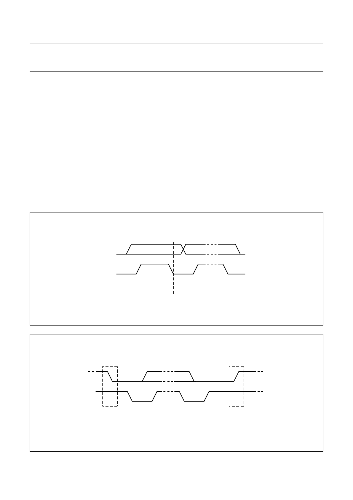
The LCD waveforms are shown in Figs 3, 4 and 5.
At frame inversion, the PCF8820 generates a dummy row
cycle, where no row is selected. This ensures equal
conditions for the first row after frame inversion as for the
other rows. Therefore the effective multiplex rate in all
modes is 1 : (multiplex rate + 1).
7.16 DDRAM to display mapping
DDRAM to display mapping is shown in Fig.6.
Linear temperature compensation is supported in the
PCF8820. The temperature coefficient for V
LCDOUT
can be
set to one of 8 values by setting bits TC2to TC0.
handbook, halfpage
V
LCD
(V)
(1) LCD characteristic.
(2) Linear temperature compensation.
0
T
amb
MGT123
(1)
(2)
(°C)
Fig.2 LCD supply voltage as a function of the
temperature.
2000 Dec 07 8
This text is here in white to force landscape pages to be rotated correctly when browsing through the pdf in the Acrobat reader.This text is here in
o
o
_white to force landscape pages to be rotated correctly when browsing through the pdf in the Acrobat reader.This text is here inThis text is here in
white to force landscape pages to be rotated correctly when browsing through the pdf in the Acrobat reader. white to force landscape pages to be ...
2000 Dec 07 9
ROW 0
ROW 0
R0(t)
R0(t)
ROW 1
ROW 1
R1(t)
R1(t)
COL 0
COL 0
C0(t)
C0(t)
COL 1
COL 1
C1(t)
C1(t)
V
V
state1
state1
V
V
state2
state2
(t)
(t)
(t)
(t)
V
V
LCD
LCD
V
V
2
2
V
V
3
3
V
V
4
4
V
V
5
5
V
V
SS
SS
V
V
LCD
LCD
V
V
2
2
V
V
3
3
V
V
4
4
V
V
5
5
V
V
SS
SS
V
V
LCD
LCD
V
V
2
2
V
V
3
3
V
V
4
4
V
V
5
5
V
V
SS
SS
V
V
LCD
LCD
V
V
2
2
V
V
3
3
V
V
4
4
V
V
5
5
V
V
SS
SS
V
V
LCD
LCD
V
V
3
3
V
V
LCD − V2
LCD − V2
0 V
0 V
V3 − V
V3 − V
V
V
LCD
LCD
V
V
3
3
V
V
LCD − V2
LCD − V2
0 V
0 V
V3 − V
V3 − V
Frame
Frame
2
2
2
2
4
4
79 16xx
79 16xx
N1
N1
N1
1
1
4
4
79 16xx
79 16xx
N1
2
2
4
4
88 16xx
88 16xx
ok, full pagewidth
ok, full pagewidth
N1
N1
3
3
N1
N1
4
4
4
4
5
5
7916xx
7916xx
88 16xx
88 16xx
N2
N2
1
1
V4 − V
V4 − V
5
5
0 V
0 V
− V5
− V5
V4 − V
V4 − V
LCD
LCD
−V
−V
LCD
LCD
V4 − V
V4 − V
5
5
0 V
0 V
− V5
− V5
V4 − V
V4 − V
LCD
LCD
−V
−V
LCD
LCD
state1
state1
state2
state2
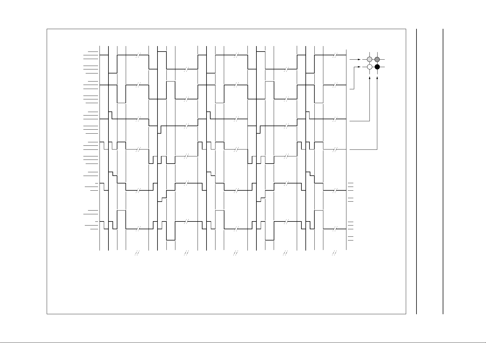
LCD driver
Philips Semiconductors Product specification
67 × 101 Grey-scale/ECB colour dot matrix
V
(t) = C1(t) − R0(t)
state1
V
(t) = C1(t) − R1(t)
state2
0012 660012 660012 660012 660012 66
0012 660012 660012 660012 660012 66
Example for setting grey-scale register.
ROW0, COL0: GS = 17
ROW1, COL0: GS = 0
ROW0, COL1: GS = 30
ROW1, COL0: GS = 63 (63 will be set to 64; see Section 8.1.8).
Fig.3 Typical LCD driver waveforms at a multiplex rate of 1 : 67.
MGT115
MGT115
PCF8820
This text is here in white to force landscape pages to be rotated correctly when browsing through the pdf in the Acrobat reader.This text is here in
o
_white to force landscape pages to be rotated correctly when browsing through the pdf in the Acrobat reader.This text is here inThis text is here in
white to force landscape pages to be rotated correctly when browsing through the pdf in the Acrobat reader. white to force landscape pages to be ...
2000 Dec 07 10
ROW 0
R0(t)
ROW 1
R1(t)
COL 0
C0(t)
COL 1
C1(t)
V
state1
V
state2
(t)
(t)
V
LCD
V
2
V
3
V
4
V
5
V
SS
V
LCD
V
2
V
3
V
4
V
5
V
SS
V
LCD
V
2
V
3
V
4
V
5
V
SS
V
LCD
V
2
V
3
V
4
V
5
V
SS
V
LCD
V
3
V
LCD − V2
0 V
V3 − V
V
LCD
V
3
V
LCD − V2
0 V
V3 − V
Frame
2
2
N1
1
N1
2
4
4
79 16xx
79 16xx
4
88 16xx
ok, full pagewidth
N1
3
N1
4
N2
1
4
5
79 16xx
88 16xx
V4 − V
5
0 V
− V5
V4 − V
LCD
−V
LCD
V4 − V
5
0 V
− V5
V4 − V
LCD
−V
LCD
state1
state2
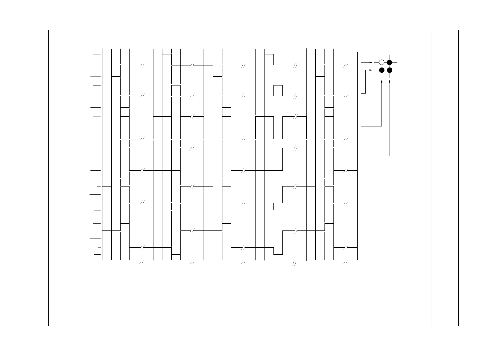
LCD driver
Philips Semiconductors Product specification
67 × 101 Grey-scale/ECB colour dot matrix
V
(t) = C1(t) − R0(t)
state1
V
(t) = C1(t) − R1(t)
state2
0012 70012 70012 7 0012 70012 7
Example for setting grey-scale register.
ROW0, COL0: GS = 17
ROW1, COL0: GS = 0
ROW0, COL1: GS = 30
ROW1, COL0: GS = 63 (63 will be set to 64; see Section 8.1.8).
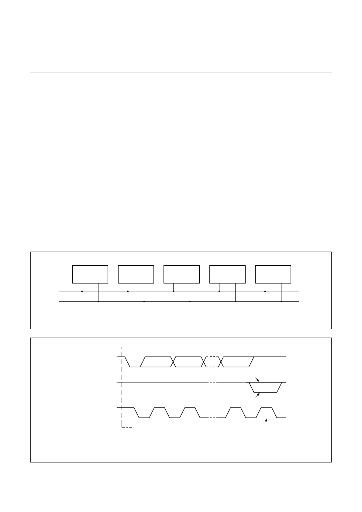
Fig.4 Typical LCD driver waveforms at a multiplex rate of 1 : 8 for partial screen mode.
MGT116
PCF8820
This text is here in white to force landscape pages to be rotated correctly when browsing through the pdf in the Acrobat reader.This text is here in
o
_white to force landscape pages to be rotated correctly when browsing through the pdf in the Acrobat reader.This text is here inThis text is here in
white to force landscape pages to be rotated correctly when browsing through the pdf in the Acrobat reader. white to force landscape pages to be ...
2000 Dec 07 11
V
state1
ROW 0
R0(t)
ROW 1
R1(t)
COL 0
C0(t)
COL 1
C1(t)
Frame
V
LCD
0.5V
LCD
V
SS
V
LCD
0.5V
LCD
V
SS
V
LCD
V
SS
V
LCD
V
SS
V
LCD
0.5V
LCD
(t)
0 V
−0.5V
LCD
−V
LCD
N1
1
N1
2
ok, full pagewidth
N1
3
N1
4
N2
1
state1
state2
LCD driver
Philips Semiconductors Product specification
67 × 101 Grey-scale/ECB colour dot matrix
V
state2
V
(t) = C1(t) − R0(t).
state1
V
(t) = C1(t) − R1(t).
state2
V
LCD
0.5V
LCD
(t)
0 V
−0.5V
LCD
−V
LCD
0012 70012 70012 7 0012 70012 7
MGT117
Example for setting grey-scale register.
ROW0, COL0: GS = 0
PCF8820
ROW1, COL0: GS = 63 (63 will be set to 64; see Section 8.1.8).
ROW0, COL1: GS = 63 (63 will be set to 64; see Section 8.1.8).
ROW1, COL0: GS = 63 (63 will be set to 64; see Section 8.1.8).
Fig.5 Typical LCD driver waveforms at a multiplex rate of 1 : 8, for partial screen mode and bias system1/2.
Philips Semiconductors Product specification
67 × 101 Grey-scale/ECB colour dot matrix
LCD driver
handbook, full pagewidth
LSB
MSB
DB0
DB1
DB2
DB3
DB4
DB5
DB6
DB7
P0
MSB
P0
LSB
P1
MSB
P1
LSB
P2
MSB
P2
LSB
P3
MSB
P3
LSB
P0
P1
P2
P3
P0
bank 0
P1
P2
P3
bank 1
bank 2
bank 3
LSB
PCF8820
pixel 0
MSB
top of LCD
R0
R4
R8
X
R = row
P = pixel
R12
.
.
.
.
.
.
bank 13
bank 14
bank 15
bank 16
X
.
.
LCD
R66
R16
R52
R56
R60
R64
MGT118
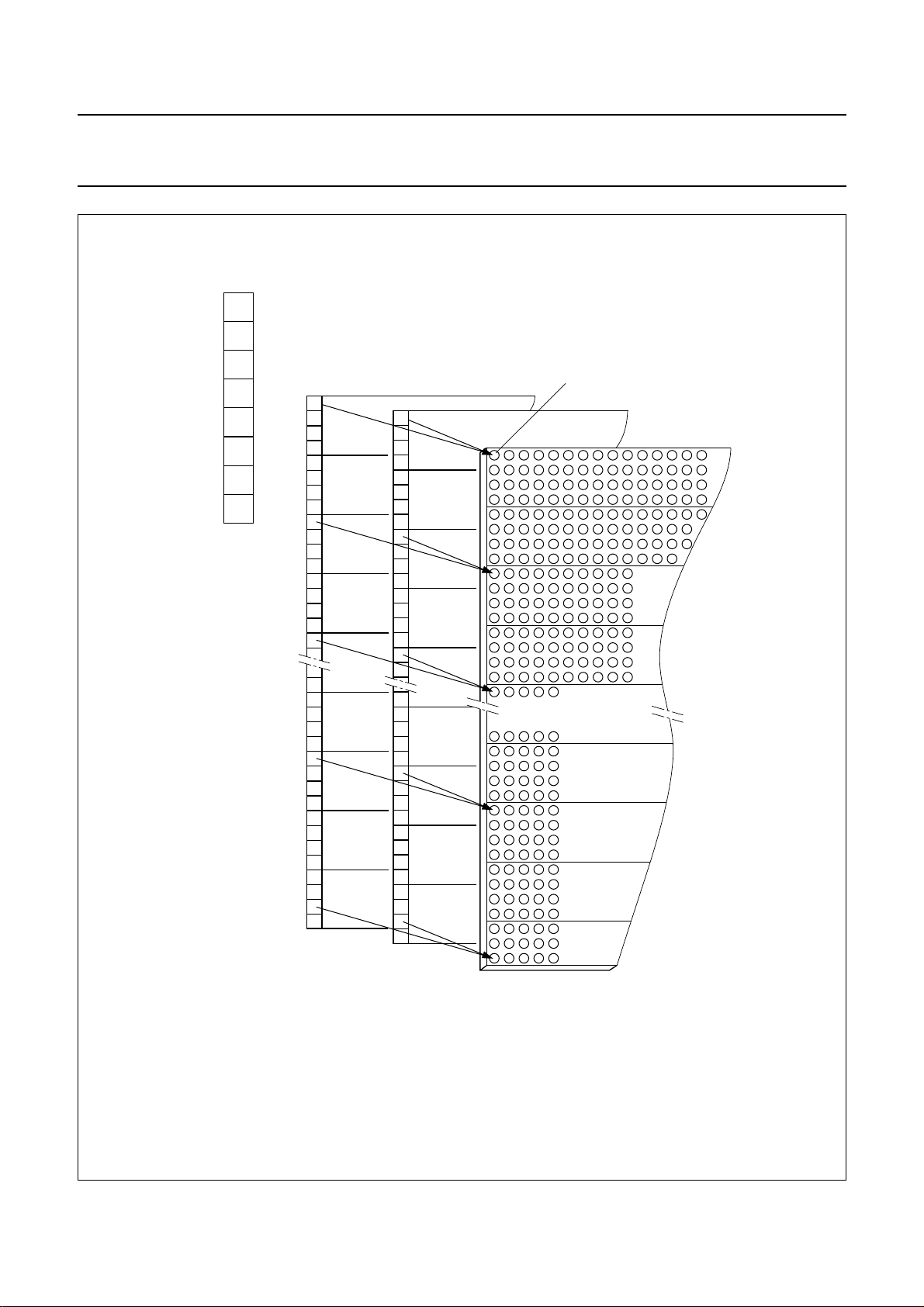
Fig.6 DDRAM to display mapping.
2000 Dec 07 12

Philips Semiconductors Product specification
67 × 101 Grey-scale/ECB colour dot matrix
LCD driver
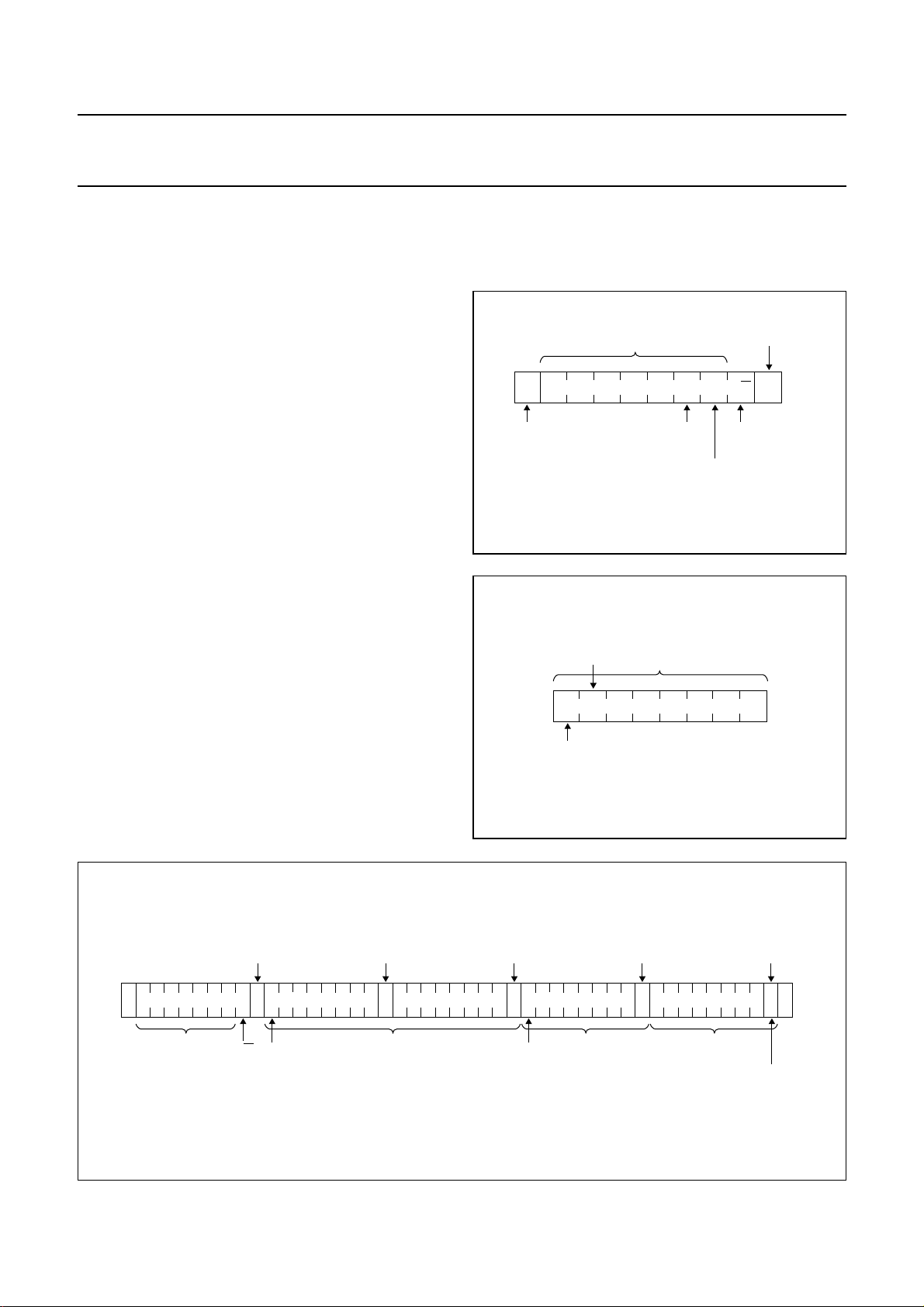
7.17 DDRAM addressing
Data is written in 8-bit bytes into the display data RAM
matrix of the PCF8820 (see Figs 6 to 8). The display data
RAMcomprisesamatrixof 67 × 101 × 2 bits. The columns
areaddressedbytheaddress pointer. The addressranges
are:X = 0 to 100 (64H) and Y=0to16(10H). It should be
noted that only 3 rows are addressed in bank 16.
Addresses outside these ranges are not allowed.
handbook, full pagewidth
LSB
Col0
MSB
PCF8820
Bit MX (see Table 3) enables or disables horizontal
address space mirroring:
• When bit MX = 0, mirroring is disabled. The address
corresponds to Col0 (see Fig.7).
• When bit MX = 1, mirroring is enabled and address
X = 0 corresponds to Col0 (see Fig.8). Bit MX
determines how data is written to the RAM. If bit MX is
changedafterwritingdatatotheRAM,nochangeonthe
display will be visible.
0
Y address
handbook, full pagewidth
LSB
MSB
0 100X address
Fig.7 RAM X-address format for mirroring disabled.
Col0
100 0
X address
16
MGT119
0
Y address
16
MGT120
Fig.8 RAM X-address format for mirroring enabled.
2000 Dec 07 13
Philips Semiconductors Product specification
67 × 101 Grey-scale/ECB colour dot matrix
LCD driver
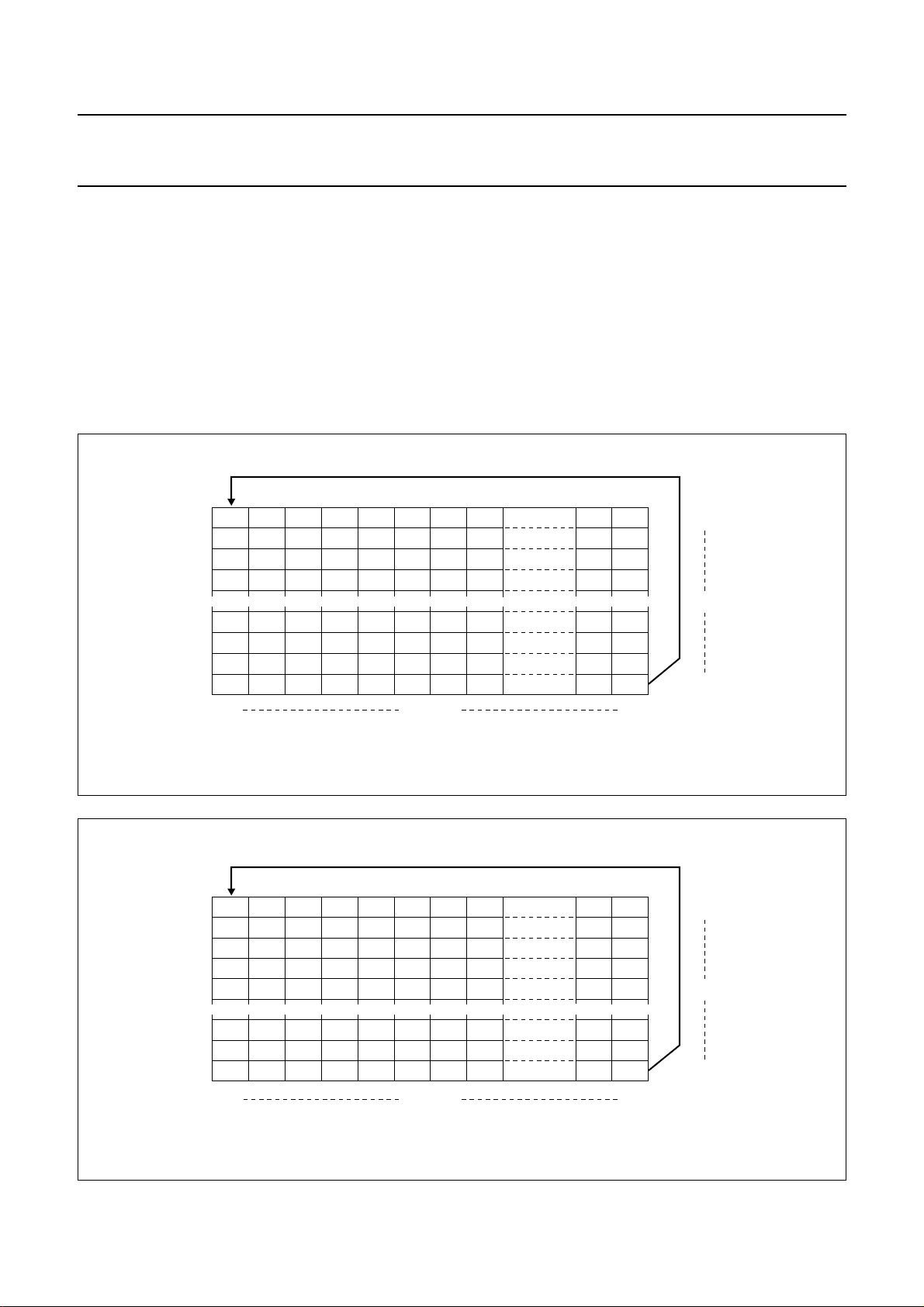
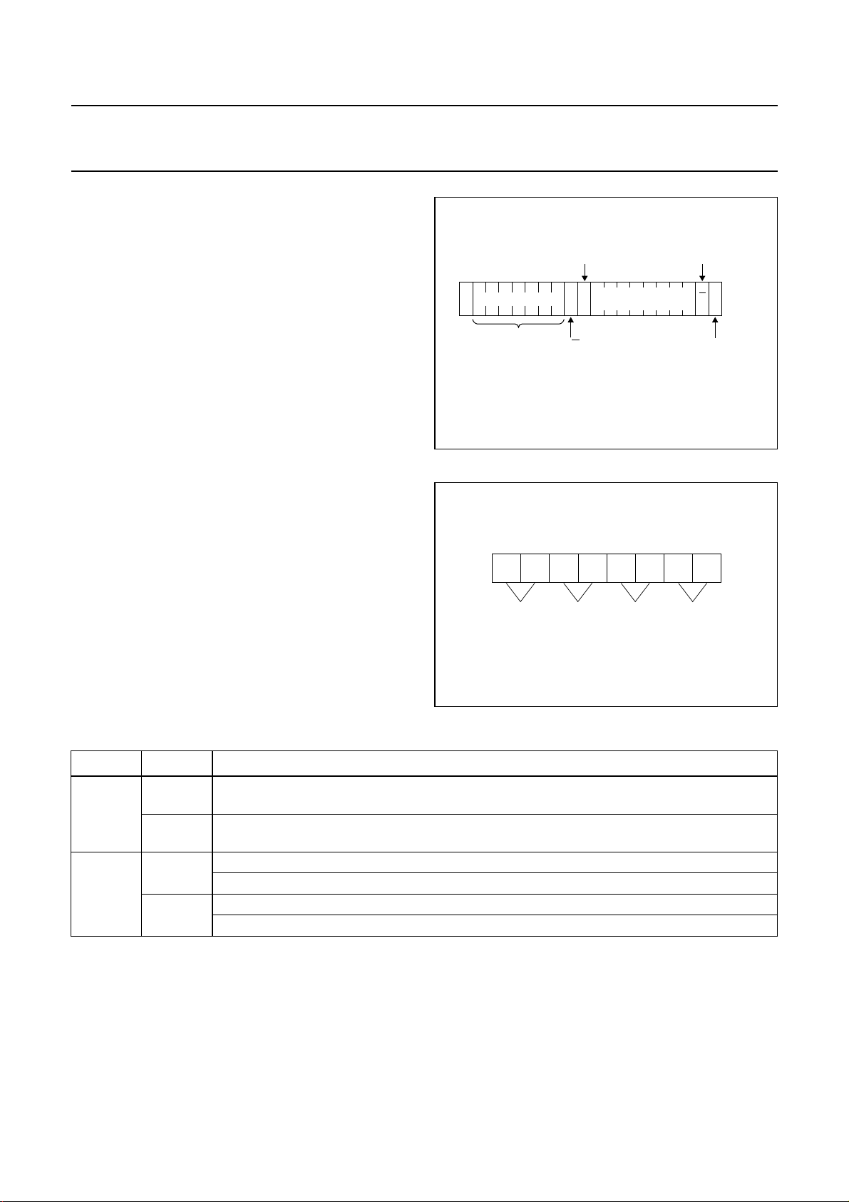
Bit V (see Table 3) selects either horizontal or vertical
address mode:
• In vertical address mode (bit V = 1), the Y-address is
incremented after each byte (see Fig.9). After Y = 16,
the Y-address sequence returns to Y = 0 and the
X-address is incremented to address the next column.
• In horizontal address mode (bit V = 0) the X-address is
incremented after each byte (see Fig.10). After X = 100,
the X-address sequence returns to X = 0 and the
Y-address is incremented to address the next row.
handbook, full pagewidth
017
118
219
320
13
14
15
16
0 100X address
PCF8820
After the very last address (X = 100 and Y = 16), the
address pointers return to the first address (X = 0 and
Y = 0). It should be noted that in bank 16 only
bits DB0 to DB5 of the data will be written into the RAM.
0
Y address
161716
MGT121
Fig.9 Writing data to RAM sequence in vertical address mode.
handbook, full pagewidth
012345 100
101 102
202 203
303 304
404
1414
1515
1616
0 100X address
Fig.10 Writing data to RAM sequence in horizontal address mode.
2000 Dec 07 14
0
201
Y address
161716
MGT122
Philips Semiconductors Product specification
67 × 101 Grey-scale/ECB colour dot matrix
LCD driver
7.18 I2C-bus interface
The I2C-bus allows bidirectional data communication
betweendifferentICsormodules. The serialdatainputline
and serial data output line are connected together, so
representing the Serial Data (SDA) line. See Section 13.4
for layout considerations. The SDA line and the Serial
Clock Line (SCL) line must be connected to a positive
supply voltage via a pull-up resistor. Data transfer may be
initiated only when the bus is not busy.
7.18.1 BIT TRANSFER
Onedatabitistransferredduringaclockpulseperiod.The
data on the SDA line must remain stable during the HIGH
periodoftheclockpulse,otherwiseanychangeinthedata
within this period will be interpreted as a control signal
(see Fig.11).
PCF8820
7.18.2 START
Both data and clock lines are HIGH when the bus is not
busy (see Fig.12).
A START condition (S) occurs when the data line goes
from HIGH-to-LOW while the clock is HIGH.
ASTOP condition (P) occurs when the data line goes from
LOW-to-HIGH while the clock is HIGH.
AND STOP CONDITIONS
handbook, full pagewidth
handbook, full pagewidth
SDA
SCL
SDA
SCL
S
START condition
data line
stable;
data valid
change
of data
allowed
Fig.11 Bit transfer.
MBC621
P
STOP condition
SDA
SCL
MBC622
Fig.12 Definition of START and STOP conditions.
2000 Dec 07 15
Philips Semiconductors Product specification
67 × 101 Grey-scale/ECB colour dot matrix
LCD driver
7.18.3 SYSTEM CONFIGURATION
Thd system components are defined below (see Fig.13):
• Transmitter: the device which sends data to the bus
• Receiver: the device which receives data from the bus
• Master: the device which initiates a transfer, generates
clock signals and terminates a transfer
• Slave: the device addressed by a master
• Multi-master: more than one master can attempt to
control the bus at the same time without corrupting the
message
• Arbitration: procedure to ensure that, if more than one
master simultaneously tries to control the bus, only one
is allowed to do so and the message is not corrupted
• Synchronization: procedure to synchronize the clock
signals of two or more devices.
7.18.4 ACKNOWLEDGE
Each 8-bit data byte transferred over the bus must be
followed by an acknowledge bit (see Fig.14).
PCF8820
Duringthe acknowledge clock pulse a HIGH-level signal is
put on the bus by the transmitter.
A slave receiver which is addressed must generate an
acknowledge bit after the reception of each data byte.
A master receiver must generate an acknowledge bit after
receiving a data byte that has been clocked out of the
slave transmitter. The device that acknowledges must
pull-down the SDA line to a LOW-level during the
acknowledge clock pulse. Set-up and hold times must be
taken into consideration to ensure that the SDA line is
stable during the HIGH period of the acknowledge related
clock pulse.
A master receiver must signal an end-of-data to the slave
transmitter by not generating an acknowledge bit on the
lastbytethathasbeenclockedoutoftheslavetransmitter.
In this event the slave transmitter must leave the data line
HIGH to allow the master to generate a STOP condition.
For the PCF8820 the acknowledge bit is output at
pad SDA_OUT.
SDA
SCL
handbook, full pagewidth
MASTER
TRANSMITTER/
RECEIVER
DATA OUTPUT
BY TRANSMITTER
DATA OUTPUT
BY RECEIVER
SCL FROM
MASTER
SLAVE
RECEIVER
S
START
condition
SLAVE
TRANSMITTER/
RECEIVER
TRANSMITTER
Fig.13 System configuration.
MASTER
not acknowledge
acknowledge
MASTER
TRANSMITTER/
RECEIVER
9821
clock pulse for
acknowledgement
MBC602
MGA807
Fig.14 Acknowledgement on the I2C-bus.
2000 Dec 07 16
Philips Semiconductors Product specification
67 × 101 Grey-scale/ECB colour dot matrix
LCD driver
7.18.5 I2C-BUS PROTOCOL
The PCF8820 is a slave transmitter/receiver. If data is to
be read from the device, the SDA_OUT output must be
used.
Before any data is transferred over the I2C-bus, the
destination device is addressed first (see Fig.15).
The PCF8820 has four 7-bit slave addresses reserved:
0111 100, 0111 101, 0111 110 and 0111 111. The two
least significant bits of the slave address are set by
connecting slave address inputs SA1 and SA0 to either
V
(logic 0) or V
SS1
A write sequence (see Fig.17) is initiated with a START
condition (S) from the I2C-bus master which is followed by
the slave address. Only the addressed slave
acknowledges. After acknowledgement, one or more
command words follow which define the status of the
addressed slave.
A command word consists of a control byte (see Fig.16)
defining ‘continuation’ bit Co and ‘register selection’
bit RS, plus a data byte. The last control byte is indicated
byresettingbit Co = 0. The control and data bytes are also
acknowledged by all addressed slaves on the bus.
Depending on the setting of bit RS in the last control byte,
either a series of display data bytes or command data
bytes may follow.
If bit RS = 1, the data bytes are stored as display data in
the DDRAM at the address specified by the data pointer.
The data pointer is automatically incremented.
If bit RS = 0, the data byte is interpreted as a command
byte to be decoded and the device will be set according to
the received commands.
DD1
(logic 1).
PCF8820
Only the addressed PCF8820 acknowledges after each
byte is received. The I
condition (P) at the end of the transmission.
S01111 SA0SA1 A
START
condition
MGU185
CoRSXXXXXX
continuation
bit
2
C-bus master issues a stop
slave address
slave
address
bit 1
Fig.15 Slave address.
register
selection
bit
control byte
Fig.16 Control byte.
slave
address
bit 0
acknowledge
bit
R/W
read/write
bit
MGT124
handbook, full pagewidth
S01111
slave address
acknowledgement
from PCF8820
S
S
A
1
A
0
0A
R/W
Co
1
RS
acknowledgement
from PCF8820
control byte
A data byte data byte
2n ≥ 0 bytes
Fig.17 Write sequence: master transmits bytes to slave receiver.
2000 Dec 07 17
acknowledgement
from PCF8820
0A AP
A
RS
Co
acknowledgement
from PCF8820
control byte
1 byte
acknowledgement
m ≥ 0 bytes
MGT125
from PCF8820
update
data pointer
Philips Semiconductors Product specification
67 × 101 Grey-scale/ECB colour dot matrix
LCD driver
For a read sequence (see Fig.18), the addressed
PCF8820 will immediately start to output the requested
data until a NOT acknowledge is transmitted by the
master. Before the read access, the user has to set bit RS
to the appropriate value by a preceding write access. The
sequence should be terminated by a STOP condition
when no further access is required, or by a RE-START
condition if further access is required.
7.18.6 COMMAND DECODER
The command decoder identifies command words
received via the I2C-bus.
Bit 7 of the control byte is named bit Co (see Fig.16):
• Bit Co = 1 indicates that only one command byte or
DDRAM data byte will follow next
• Bit Co = 0 indicates that a stream of command bytes or
DDRAM data bytes will follow next depending on last
status of bit RS.
Bit 6 of a control byte is named bit RS:
• Bit RS = 1 indicates that another DDRAM data byte will
follow next
• Bit RS = 0 indicates that another command byte will
follow next.
The definition of bits Co and RS is shown in Table 1.
PCF8820
acknowledgement
from PCF8820
S
S01111
slave address
S
A
1
A
0
1A
R/W
Fig.18 Read sequence: master receives bytes
from slave transmitter status register.
MSB LSB
DB7 DB6 DB5 DB4 DB3 DB2 DB1 DB0
P3
P3
LSB
MSBP2LSBP2MSBP1LSBP1MSBP0LSBP0MSB
pixel 3 pixel 2 pixel 1 pixel 0
not acknowledgement
temperature
readout value
from master
AP
STOP condition
MGT126
MGT127
7.18.7 DISPLAY DATA BYTE
Fig.19 Grey-scale display data byte.
A display data byte for grey-scale is shown in Fig.19.
Table 1 Definition of bits Co and RS
BIT VALUE ACTION
Co 0 last control byte to be sent; only a stream of data bytes are allowed to follow; this stream may
only be terminated by a STOP or RE-START condition
1 another control byte will follow the data byte unless a STOP or RE-START condition is
received
RS 0 data byte will be decoded and used to set up the device
data byte will return the sensor temperature read-out
1 data byte will be stored in the DDRAM
RAM read-back (not supported)
2000 Dec 07 18
 Loading...