

Philips PCF8812U-2 Datasheet

INTEGRATED CIRCUITS
DATA SH EET
PCF8812
65 × 102 pixels matrix LCD driver
Product specification
File under Integrated Circuits, IC12
2000 Nov 22

Philips Semiconductors Product specification
65 × 102 pixels matrix LCD driver PCF8812
CONTENTS
1 FEATURES
2 APPLICATIONS
3 GENERAL DESCRIPTION
4 ORDERING INFORMATION
5 BLOCK DIAGRAM
6 PINNING
7 PIN FUNCTIONS
7.1 Pin functions
7.1.1 ROW 0 to ROW 64 row driver outputs
7.1.2 COL 0 to COL 101 column driver outputs
7.1.3 V
7.1.4 V
7.1.5 V
7.1.6 V
7.1.7 V
and V
SS1
DD1
LCDIN
LCDOUT
LCDSENSE
(V
LCD
SS2
to V
DD3
: LCD power supply
: LCD power supply
: voltage multiplier regulation input
)
: negative power supply rails
: positive power supply rails
7.1.8 T1 to T5: test pads
7.1.9 SDIN: serial data line
7.1.10 SCLK: serial clock line
7.1.11 D/C: mode select
7.1.12 SCE: chip enable
7.1.13 OSC: oscillator
7.1.14 RES: reset
8 FUNCTIONAL DESCRIPTION
8.1 Oscillator
8.2 Address Counter (AC)
8.3 Display Data RAM (DDRAM)
8.4 Timing generator
8.5 Display address counter
8.6 LCD row and column drivers
9 ADDRESSING
9.1 Data structure
10 INSTRUCTIONS
10.1 Initialization
10.2 Reset function
10.3 Function set
10.3.1 PD
10.3.2 V
10.3.3 H
10.4 Display control
10.4.1 D and E
10.5 Set Y address of RAM
10.6 Set X address of RAM
10.7 Set HV-generator stages
10.8 Bias system
10.9 Temperature control
10.10 Set VOP value
11 LIMITING VALUES
12 HANDLING
13 DC CHARACTERISTICS
14 AC CHARACTERISTICS
15 SERIAL INTERFACE
16 RESET
17 APPLICATION INFORMATION
18 CHIP INFORMATION
19 PAD INFORMATION
20 BONDING PAD LOCATION
21 DEVICE PROTECTION DIAGRAM
22 TRAY INFORMATION
23 DATA SHEET STATUS
24 DEFINITIONS
25 DISCLAIMERS
2000 Nov 22 2
Philips Semiconductors Product specification
65 × 102 pixels matrix LCD driver PCF8812
1 FEATURES
• 65 row and 102 column outputs
• Display data RAM 65 × 102 bits
• On-chip:
– Configurable 5 (4, 3 and 2) voltage multiplier
generating V
(external V
LCD
also possible)
LCD
– Generation of intermediate LCD bias voltages
– Oscillator requires no external components
(external clock also possible).
• External reset input pin
• Serial interface maximum 4.0 Mbit/s
• CMOS compatible inputs
• Mux rate: 1 : 65
• Logic supply voltage range V
DD1
to VSS:
– 2.5 to 5.5 V.
• High voltage generator supply voltage range
V
to VSS and V
DD2
DD3
to V
SS
– 2.5 to 4.5 V.
• Display supply voltage range V
LCD
to VSS:
– 4.5 to 9.0 V.
• Low power consumption, suitable for battery operated
systems
• Temperature compensation of V
• Temperature range: T
amb
LCD
= −40 to +85 °C
• Slim chip layout, suited for Chip-On-Glass (COG)
applications.
2 APPLICATIONS
• Telecom equipment.
3 GENERAL DESCRIPTION
The PCF8812is a low power CMOS LCD controller driver,
designed to drive a graphic display of 65 rows and
102 columns. All necessary functions for the display are
provided in a single chip, including on-chip generation of
LCD supply and bias voltages, resulting in a minimum of
external components and low power consumption. The
PCF8812 interfaces to microcontrollers via a serial bus
interface.
4 ORDERING INFORMATION
PACKAGE
TYPE NUMBER
NAME DESCRIPTION VERSION
PCF8812U/2 Tray chip with bumps in tray −
2000 Nov 22 3
Philips Semiconductors Product specification
65 × 102 pixels matrix LCD driver PCF8812
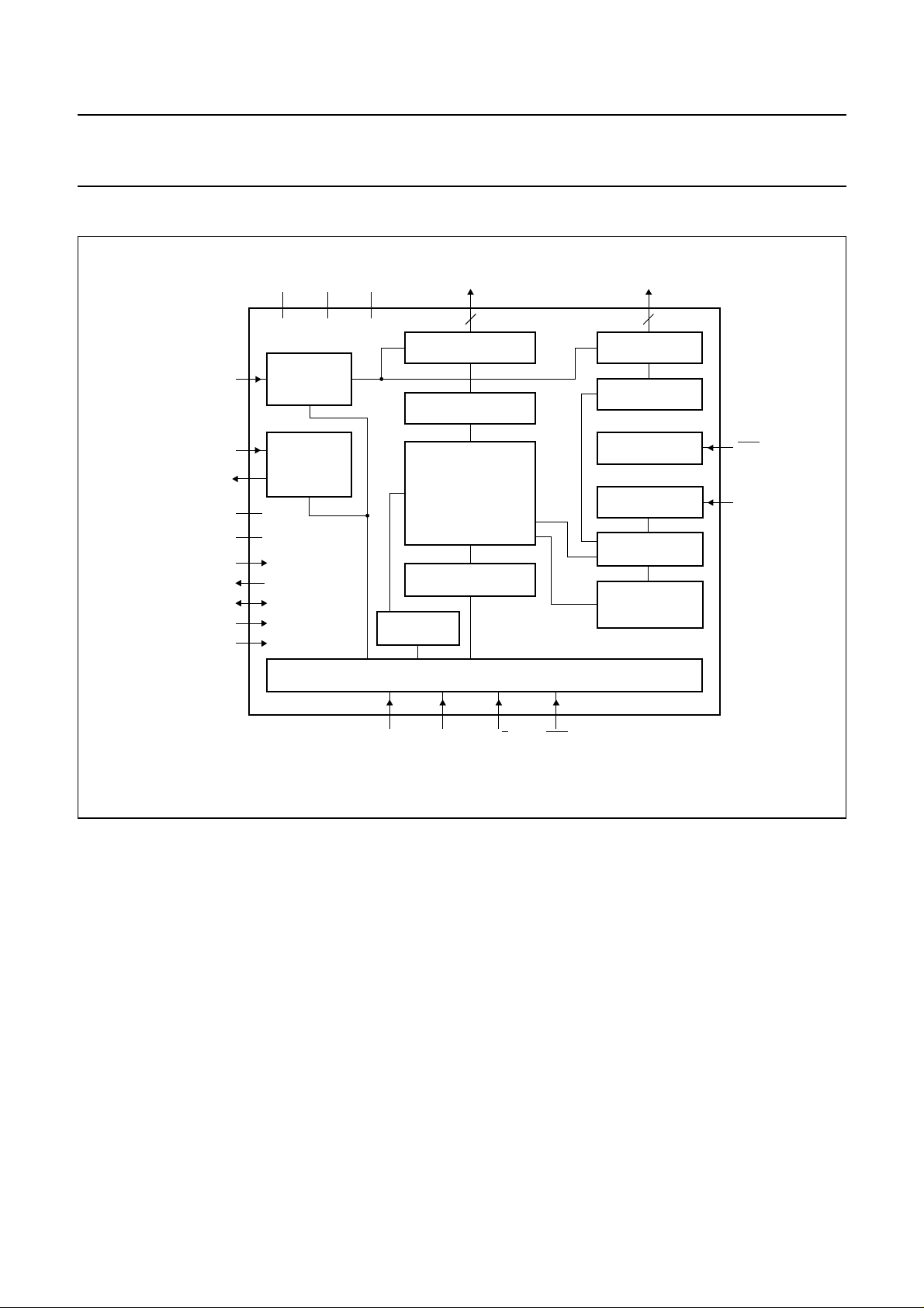
5 BLOCK DIAGRAM
V
handbook, full pagewidth
DD1
V
DD2VDD3
COL0 to COL101
ROW0 to ROW64
V
LCDIN
V
LCDSENSE
V
LCDOUT
V
V
SS1
SS2
T1
T2
T3
T4
T5
BIAS
VOLTAGE
GENERATOR
HIGH
VOLTAGE
GENERATOR
4 stages
COLUMN DRIVERS
DATA LATCHES
DISPLAY DATA RAM
65 × 102 bits
ADDRESS COUNTER
DATA
REGISTER
SDIN SCLK
102
(DDRAM)
I/O BUFFER
D/C
PCF8812
SCE
65
ROW DRIVERS
SHIFT REGISTER
RESET
OSCILLATOR
TIMING
GENERATOR
DISPLAY
ADDRESS
COUNTER
RES
OSC
MGT636
Fig.1 Block diagram.
2000 Nov 22 4
Philips Semiconductors Product specification
65 × 102 pixels matrix LCD driver PCF8812
6 PINNING 7 PIN FUNCTIONS
SYMBOL PAD DESCRIPTION
RES 1 external reset input
(active LOW)
ROW 32 to
2 to 15 LCD row driver outputs
ROW 19
ROW 0 to
18 to 36 LCD row driver outputs
ROW 18
COL0to
COL 101
ROW 50 to
37 to 138 LCD column driver
outputs
139 to 156 LCD row driver outputs
ROW 33
ROW 51 to
159 to 172 LCD row driver outputs
ROW 64
V
V
V
DD1
DD3
DD2
174 to 179 supply voltage 1
180 supply voltage 3
181 to 193 supply voltage 2
OSC 194 oscillator input
SDIN 195 serial data input
D/
C 196 data/command input
SCE 197 chip enable input
(active LOW)
T2 198 test 2 output
SCLK 199 serial clock input
V
SS2
V
SS1
200 to 213 negative power supply 2
214 to 217 negative power supply 1
T1 218 test 1 input
T5 219 test 5 input
T4 220 test 4 input
V
SS1
221 and 222 negative power supply 1
T3 223 test 3 input/output
V
LCDIN
V
LCDOUT
V
LCDSENSE
224 to 229 LCD supply voltage
230 to 236 voltage multiplier output
237 voltage multiplier
regulation input (V
16, 17, 157,
dummy pads
158 and 173
LCD
7.1 Pin functions
7.1.1 ROW 0 TO ROW 64 ROW DRIVER OUTPUTS
These pads output the row signals.
7.1.2 COL 0 TO COL 101 COLUMN DRIVER OUTPUTS
These pads output the column signals.
7.1.3 V
The 2 supply rails V
SS1
AND V
: NEGATIVE POWER SUPPLY RAILS
SS2
SS1
and V
must be connected
SS2
together.
7.1.4 V
V
and V
DD2
TO V
DD1
are the supply voltage for the internal
DD3
: POSITIVE POWER SUPPLY RAILS
DD3
voltage generator. Both have the same voltage and may
be connected together outsideof thechip. V
supply for the rest of the chip. V
together with V
DD2
and V
DD3
can be connected
DD1
but in thiscase care must be
is used as
DD1
taken to respect the supply voltage range
(see Chapter 13).
If the internal voltage generator is not used then V
V
must be connected to V
DD3
7.1.5 V
: LCD POWER SUPPLY
LCDIN
or connected to power.
DD1
DD2
and
Positive power supply for the liquid crystal display.
An external LCDsupply voltage canbe supplied using the
V
pad. In thiscase V
LCDIN
LCDOUT
has to beleft open-circuit
and the internal voltage generator has to be programmed
to zero. If the PCF8812 is in Power-down mode, the
external LCD supply voltage has to be switched off.
7.1.6 V
: LCD POWER SUPPLY
LCDOUT
Positive power supply for the liquid crystal display. If the
internal voltage generator is used, the two supply rails
V
LCDIN
and V
must be connected together. If an
LCDOUT
external supply is used this pin must be left open-circuit.
)
7.1.7 V
V
LCDSENSE
LCDSENSE
INPUT
is the input of the internal voltage multiplier
: VOLTAGE MULTIPLIER REGULATION
(V
)
LCD
regulation.
2000 Nov 22 5
If the internal voltage generator is used then V
mustbe connectedtoV
is used then the V
LCDSENSE
.If aexternalsupply voltage
LCDOUT
can be let open-circuit or
connected to ground.
LCDSENSE

Philips Semiconductors Product specification
65 × 102 pixels matrix LCD driver PCF8812
7.1.8 T1 TO T5: TEST PADS
T1, T3, T4 and T5 must be connected to VSS, T2 must be
left open-circuit. Not accessible to user.
7.1.9 SDIN: SERIAL DATA LINE
Serial data input line.
7.1.10 SCLK: SERIAL CLOCK LINE
Input for the clock signal 0 to 4.0 Mbits/s.
7.1.11 D/C: MODE SELECT
Input to select either command/address or data input.
7.1.12 SCE: CHIP ENABLE
The enable pin allows data to be clocked in; the signal is
active LOW.
7.1.13 OSC: OSCILLATOR
When the on-chip oscillator is used this input must be
connected to VDD. An external clock signal, if used, is
connected to this input. If the oscillator and external clock
are both inhibited by connecting the OSC pin to VSS the
display is not clocked and may be left in a DC state.
To avoid this the chip should always be put into
Power-down mode before stopping the clock.
7.1.14 RES: RESET
8.2 Address Counter (AC)
The address counter assigns addresses to the display
data RAM for writing. The X address X6 to X0 and the
Y address Y3 to Y0 are set separately. After a write
operation the address counter is automatically
incremented by 1 according to the V flag (see Chapter 9).
8.3 Display Data RAM (DDRAM)
The PCF8812 contains a 65 × 102 bit static RAM which
storesthe displaydata. TheRAM is dividedinto 8 banksof
102 bytes (8 × 8 × 102 bits) and one bank of 102 bits
(1 × 102 bits). During RAM access, data is transferred to
the RAM via the serial interface. There is a direct
correspondence between the X address and the column
output number.
8.4 Timing generator
The timing generator produces the various signals
required to drive the internal circuitry. Internal chip
operation is not affected by operations on the data buses.
8.5 Display address counter
The display is generated by continuously shifting rows of
RAM data to the dot matrix LCD via the column outputs.
The display status (all dots on/off and normal/inverse
video) is set by bits E and D in the command ‘display
control’ (see Table 2).
This signal will reset the device and must be applied to
properly initialize the chip; the signal is active LOW.
8 FUNCTIONAL DESCRIPTION
8.1 Oscillator
The on-chip oscillator provides the clock signal for the
display system.No external componentsare required and
the OSC input must be connected to VDD. An external
clock signal, if used, is connected to this input.
2000 Nov 22 6
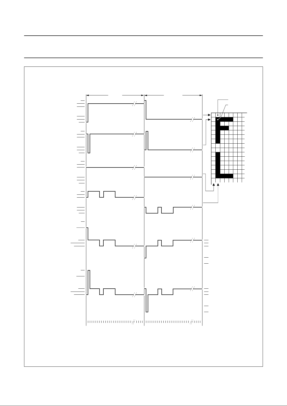
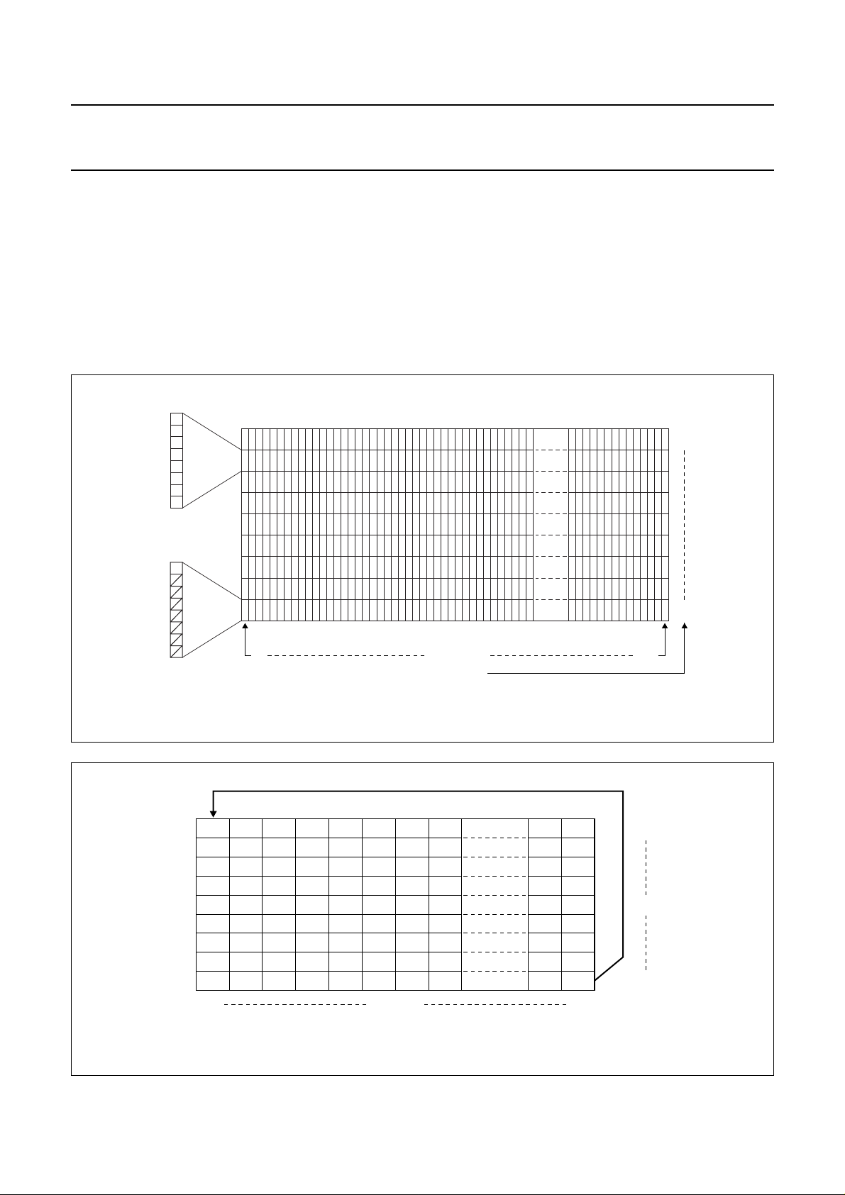
8.6 LCD row and column drivers
The PCF8812 contains 65 row and 102 column drivers,
which connect the appropriate LCD bias voltages in
sequence to the display in accordance with the data to be
displayed. Figure 2 shows typical waveforms. Unused
outputs should be left unconnected.
Philips Semiconductors Product specification
65 × 102 pixels matrix LCD driver PCF8812
ROW 0
R0 (t)
ROW 1
R1 (t)
COL 0
C0 (t)
COL 1
C1 (t)
V
V3 − V
LCD
− V
SS
V
V
V
V
V
V
V
V
V
V
V
V
V
V
V
V
V
V
V
V
V
V
V
V
LCD
2
3
4
5
SS
LCD
2
3
4
5
SS
LCD
2
3
4
5
SS
LCD
2
3
4
5
SS
SS
frame n frame n + 1
V
state1
V
state2
(t)
(t)
V
− V
LCD
0 V
V3 − V
V
LCD
V3 − V
V
LCD
0 V
V3 − V
2
− V
SS
− V
2
2
SS
2
012345678... ... 64 012345678... ... 64
(1) V
(2) V
V
state1
V
state2
(t) = C1(t) − R0(t).
state1
(t) = C1(t) − R1(t).
state2
(t)
(t)
Fig.2 Typical LCD driver waveforms.
2000 Nov 22 7
V4 − V
0 V
VSS − V
V4 − V
V
SS
V4 − V
0 V
VSS − V
V4 − V
V
SS
MGT637
− V
− V
5
5
LCD
LCD
5
5
LCD
LCD

Philips Semiconductors Product specification
65 × 102 pixels matrix LCD driver PCF8812
DDRAM
bank 0
top of LCD
bank 1
bank 2
bank 3
bank 7
bank 8
LCD
Fig.3 DDRAM to display mapping.
2000 Nov 22 8
MGS395
Philips Semiconductors Product specification
65 × 102 pixels matrix LCD driver PCF8812
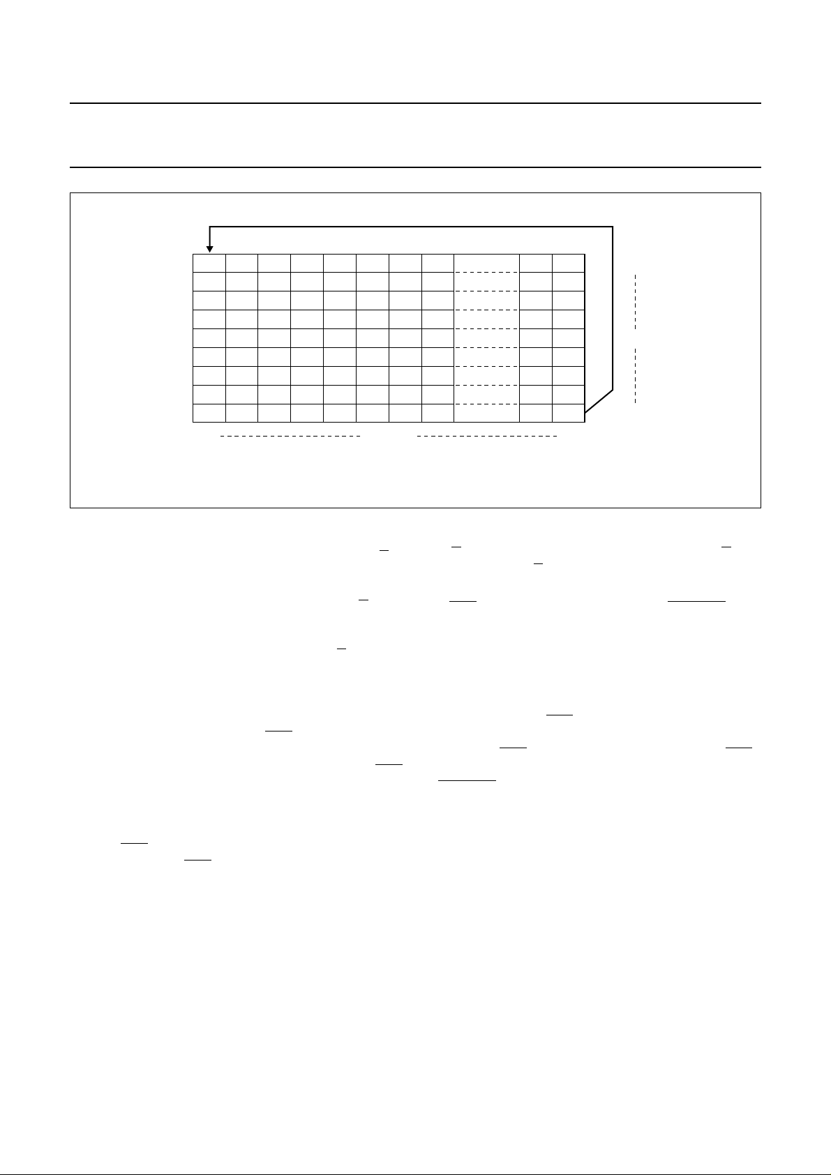
9 ADDRESSING
Data is downloaded in bytes into the RAM matrix of the PCF8812 as indicated in Figs.3, 4, 5 and 6. The display RAM
has a matrix of 65 × 102 bits. The columns are addressed by the address pointer. The address ranges are: X0 to X101
(1100101) andY0 to Y8 (1000). Addresses outside of these ranges are not allowed.In vertical addressingmode (V = 1)
the Y address increments after each byte (see Fig.6). After the last Y address (Y = 8) Y wraps around to 0 and X
increments toaddress the nextcolumn. In horizontaladdressing mode (V = 0)the X address incrementsafter each byte
(see Fig.5). After the last X address (X = 101) X wraps around to 0 and Y increments to address the next row. After the
very last address (X = 101 and Y = 8) the address pointers wrap around to address (X = 0 and Y = 0).
9.1 Data structure
handbook, full pagewidth
handbook, full pagewidth
MSB
LSB
MSB
LSB
0 101X address
Fig.4 RAM format addressing.
09
110
2
3
4
5
6
7
8
0 101X address
Y address
0
8
MGT638
0
Y address
8917
MGS397
Fig.5 Sequence of writing data bytes into RAM with vertical addressing (V = 1).
2000 Nov 22 9
Philips Semiconductors Product specification
65 × 102 pixels matrix LCD driver PCF8812
handbook, full pagewidth
012
102 103 104
204 205 206
306 307 308
408 409 410
510 511 512
612 613 614
714 715 716
816 817 818
0 101X address
Fig.6 Sequence of writing data bytes into RAM with horizontal addressing (V = 0).
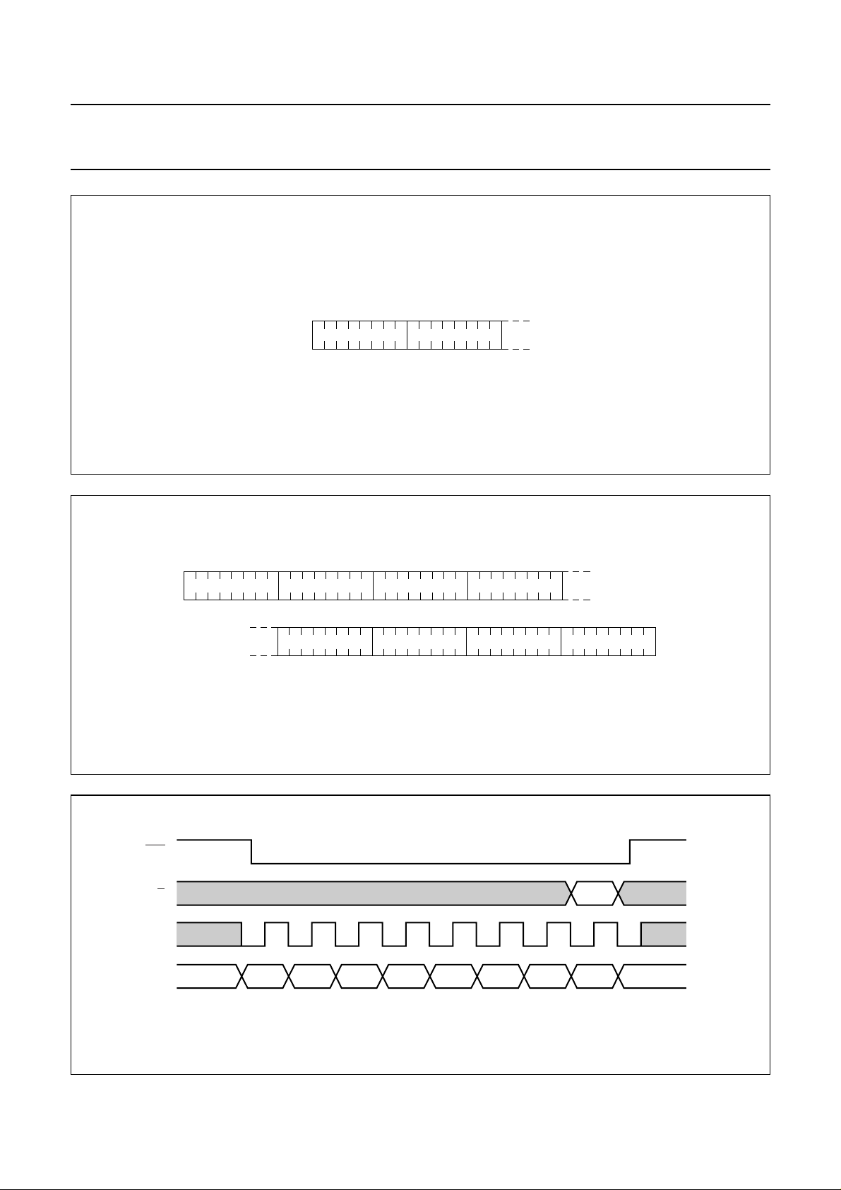
10 INSTRUCTIONS
The instruction format is divided into two modes: If D/C
(mode select) is setLOW thecurrent byteis interpreted as
command byte(see Table 1). Figure 8 showsan example
of a serial datastream for initializing the chip. If D/C is set
HIGH the following bytes are stored in the display data
RAM. After every data byte the address counter is
incremented automatically. The level of the D/C signal is
read during the last bit of the data byte. Every instruction
can be sent in any order to the PCF8812. The MSB of a
byte is transmitted first. Figure 8 shows one possible
command stream, used to set-up the LCD driver. The
serial interface is initialized when SCE is HIGH. In this
state SCLK clock pulses have no effect and no power is
consumedby theserial interface. A negativeedge onSCE
enablesthe serialinterface andindicatesthe startofa data
transmission.
0
Y address
8917
MGS396
• SDIN is sampled at the positive edge of SCLK
• D/C indicates whether the byte is acommand (D/C=0)
or RAM data (D/C = 1). It is read with the eighth SCLK
pulse
• If SCE stays LOW after the last bit of a command/data
byte, theserial interfaceexpects DB7 of the nextbyte at
the next positive edge of SCLK (see Fig.12). If SCLK
goes LOW after the last data bit (DB0), either:
– A rising clock edge is requiredto latchthe lastdata bit
– Or the last bit is latched when SCE goes HIGH.
• A reset pulse with RES interrupts the transmission.
No data is written into the RAM. The registers are
cleared. If SCE is LOW after the positive edge of RES,
the serial interface is ready to receive bit 7 of a
command/data byte (see Fig.12).
Figures 9 and 10 show the serial bus protocol:
• When SCE is HIGH, SCLK clocks are ignored. During
the HIGH time of SCE the serial interface is initialized
(see Fig.12)
2000 Nov 22 10
Philips Semiconductors Product specification
65 × 102 pixels matrix LCD driver PCF8812
handbook, full pagewidth
handbook, halfpage
MSB (DB7) LSB (DB0)
Fig.7 General format of data stream.
bias systemfunction set (H = 1)
set V
OP
datadata
MGT639
temperature control
X addressY addressdisplay controlfunction set (H = 0)
MGT640
Fig.8 Example of serial data stream.
handbook, full pagewidth
SCE
D/C
SCLK
SDIN
DB7 DB6 DB5 DB4 DB3 DB2 DB1 DB0
Fig.9 Serial bus protocol transmission of one byte.
2000 Nov 22 11
MGT641
 Loading...