

Philips PCF8801 Datasheet

INTEGRATED CIRCUITS
DATA SH EET
PCF8801
LCD driver for 140 × 2 segments
Product specification
File under Integrated Circuits, IC12
2000 Feb 04

Philips Semiconductors Product specification
LCD driver for 140 × 2 segments PCF8801
FEATURES
• Single-chip LCD controller/driver
• Fixed backplane multiplexing at a rate of 1 : 2
• Internal LCD bias generation (0.5VDD)
• 140 segment outputs configured to drive seven
40-segment characters
• On-chip oscillator with one external resistor
• Wide power supply range (2.7 V up to 5.5 V)
• Low power consumption
• Compatible with most microprocessors/microcontrollers
• 1 MHz serial bus interface (280-bit shift register)
• Easily cascaded for large LCD applications (two
cascade directions possible)
• Compatible with chip-on-glass technology
• Manufactured by silicon gate CMOS process.
GENERAL DESCRIPTION
The PCF8801 is a peripheral device which interfaces a
multiplexed Liquid Crystal Display (LCD) having two
backplanes and up to 140 segments. It generates drive
signals at a multiplex rate of 1 : 2 allowing seven
40-segment (5 x 8) characters to be driven.
The chip can easily be cascaded for larger LCD
applications,andthedirectionoftheinformationflowinthe
cascadecanbeselected.ThePCF8801iscompatiblewith
most microprocessors/microcontrollers and
communicates via a serial bus interface comprising a
280-bit shift register.
Theoutputsaremultiplexedbyaclocksignalgeneratedby
the internal oscillator which needs only one external
resistor.Cascadeapplicationsonlyrequiretheclocksignal
to be generated by the first device with the internal
oscillators in the other devices disabled.
The PCF8801 is designed for chip-on-glass applications.
It has a narrow package with raised points (bumps) for
easy assembly on to LCD glass.
ORDERING INFORMATION
TYPE
NUMBER
PCF8801U − chip with bumps in tray −
NAME DESCRIPTION VERSION
PACKAGE
2000 Feb 04 2
Philips Semiconductors Product specification
LCD driver for 140 × 2 segments PCF8801
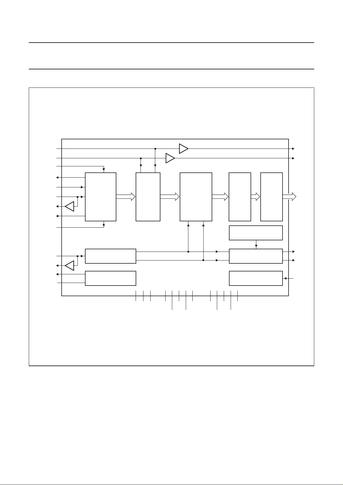
BLOCK DIAGRAM
handbook, full pagewidth
LDPI
LDNI
DI1
DO1
DIR
CLKI
CLKO
DO2
280-BIT
BI-
DIRECTIONAL
SHIFT
REGISTER
SH1_1
SH140_2
280-BIT
OUTPUT
REGISTER
IO1_1
IO140_2
OUTPUT
MULTIPLEXER
OM1
OM140
ROUTING
BLOCK
OUTPUT
DRIVERS
LDPO
LDNO
S1
S140
DI2
OSCI
OSCO
INT_OSCO
REXT
LCD BIAS GENERATOR
V
÷2
÷4
INTERNAL OSCILLATOR POWER-ON-RESET
T2 T3
T1
PCF8801
V
V
SS1
SS3VSS5VDD1
V
SS2VSS4
COMMON
M
V
V
DD2VDD4
BACKPLANE DRIVERSFRAME GENERATOR
DD3VDD5
MID
Fig.1 Block diagram.
COM1
COM2
RESET
MGL915
2000 Feb 04 3
Philips Semiconductors Product specification
LCD driver for 140 × 2 segments PCF8801
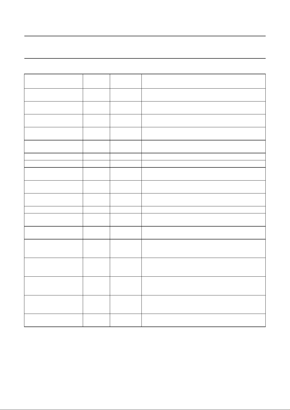
PINNING
SIMPLIFIED
SYMBOL
DD
(1)
DESCRIPTION
Power supply for output drivers, backplane drivers and LCD
V
DD1
SYMBOL PAD
to V
DD4
28, 27, 3, 4 V
bias generator; 4 pads connected internally
V
SS1
to V
SS4
30, 29, 1, 2 V
SS
Ground for output drivers, backplane drivers and LCD bias
generator; 4 pads connected internally
V
V
DD5
SS5
16 V
15 V
DD
SS
Power supply for remaining circuitry; connect externally to
V
to V
DD1
DD4
Ground for remaining circuitry; connect externally to
V
to V
SS1
SS4
REXT 10 Enable internal oscillator input; connected via an external
resistor
RESET 14 Reset input; active HIGH
T1 to T3 13, 17, 18 Test pads; must remain unconnected
COM1_1, COM1_2 31, 173 COM1 First pair of identical 3-level LCD backplane outputs; each
pad is located on opposite sides of the die
COM2_1, COM2_2 32, 174 COM2 Second pair of identical 3-level LCD backplane outputs;
each pad is located on opposite sides of the die
DIR 19 Data direction control input; its voltage level determines the
direction in which data is shifted
S1 to S140 33 to 172 LCD driver outputs
DI1, DI2 24, 7 DI Data input; the status of DIR determineswhich pad is valid;
each pad is located on opposite sides of the die
DO1, DO2 23, 8 DO Data outputs; both identical; both always valid; for cascade
use; each pad is located on opposite sides of the die
LDP1, LDP2 26, 5 LDPI, LDPO Data load control input (LDPI) and output (LDPO) on rising
edge; the status of DIR determines which pad is valid; each
pad is located on opposite sides of the die
LDN1, LDN2 25, 6 LDNI, LDNO Data load control input (LDNI) and output (LDNO) on falling
edge; the status of DIR determines which pad is valid; each
pad is located on opposite sides of the die
CLK1, CLK2 22, 9 CLKI, CLKO Data shift clock input (CLKI) and output (CLKO); the status
of DIR determineswhich pad is valid; for cascade use; each
pad is located on opposite sides of the die
OSC1, OSC2 21, 11 OSCI, OSCO LCD multiplexing clock input (OSCI) and output (OSCO);
the status of DIR determines which pad is valid; each pad is
located on opposite sides of the die
INT_OSCO1, INT_OSCO2 20, 12 INT_OSCO Internal oscillator outputs; both identical; each pad is
located on opposite sides of the die
Note
1. These symbols simplify descriptions in this data sheet where several pads have the same function and also indicate
the direction of data on pads which can be selected to be either an input or an output.
2000 Feb 04 4

Philips Semiconductors Product specification
LCD driver for 140 × 2 segments PCF8801
FUNCTIONAL DESCRIPTION
Refer to block diagram Fig.1. The PCF8801 comprises a
bi-directional 280-bit input shift register, 280-bit output
register,output multiplexer providing140-segmentoutputs
via a routing block and output drivers, two 3-level
backplane outputs, internal oscillator and internal
power-on reset circuit. To reduce the length of routing
requiredbetween cascaded chipsinmultiple chip-on-glass
applications, all inputs/outputs for control lines, clock
signals and data are provided at both sides of the narrow
package.
Shift register
The 280-bit bi-directional shift register shifts data on the
rising edge of clock signal CLKI. The shift register output
bits are called SH1_1, SH1_2 to SH140_1, SH140_2.
The direction in which data is shifted and the pads that are
valid for inputs DI, CLKI and output CLKO, is determined
by the voltage level on pad DIR. The voltage on pad DIR
mustbe tied to either VDDorVSSandmust not be switched
when the PCF8801 is operating. Therelationship between
the status of pad DIR and the other pads connected to the
shift register is shown in Table 1.
Table 1 280-bit bi-directional shift register pads
VALID PAD
SHIFT DIRECTION
DIR = 1 DIR = 0
Data input DI
(1)
Data output DO
(2)
DI1 DI2
DO1 and DO2 DO1 and DO2
Clock input CLKI CLK1 CLK2
Clock output CLKO
(2)
CLK2 CLK1
First bit shifted SH140_2 SH1_1
Last bit shifted
(3)
SH1_1 SH140_2
Notes
1. The invalid DI pad must be connected to either VDDor
VSS.
2. Pads DOand CLKO are used when PCF8801devices
are connected in cascade.
3. The last bit is loaded into a flip-flop whose output is
connectedtopad DO.Thevalue of the last bit appears
at pad DO delayed by a1⁄2CLKI period.
Output register
The280-databits(SH1_1,SH1_2 to SH140_1, SH140_2)
from the output of the shift register are transferred to the
input of the 280 bit output register. Data is transferred
when either pad LDPI goes HIGH or when pad LDNI goes
LOW. The output register bits are called IO1_1, IO1_2
to IO140_1, IO140_2. The pads that are valid for
inputs LDPI, LDNI, OSCI, and outputs LDPO, LDNO,
OSCO are determined by the voltage level on pad DIR.
During a positive pulse on pad LDPI, pad LDNI must stay
HIGH, or during a negative pulse on pad LDNI, pad LDPI
must stay LOW. The voltage on pad DIR must be tied to
either VDD or VSS and must not be switched when the
PCF8801 is operating. The relationship between the
status of pad DIR and the other pads connected to the
output register is shown in Table 2.
Table 2 280-bit output register pads
VALID PAD
SHIFT DIRECTION
DIR = 1 DIR = 0
Data load input LDPI LDP1 LDP2
Data load output LDPO LDP2 LDP1
Data load input LDNI LDN1 LDN2
Data load output LDNO LDN2 LDN1
Multiplexing clock input OSCI OSC1 OSC2
Multiplexing clock output OSCO OSC2 OSC1
Output multiplexer, frame generator and backplane
drivers
The 280 data bits (IO1_1, IO1_2 to IO140_1, IO140_2)
from the output register are transferred to the input of the
output multiplexer which multiplexes the data at the rate of
1 : 2. The 140 output bits from the output multiplexer are
called OM1 to OM140. The frame generator outputs two
control signals derived from the LCD multiplex clock
(OSCI) called COMMON (1⁄2f
) and M (1⁄4f
OSC
OSC
) which
control the output multiplexer and the backplane drivers.
The operation of the output multiplexer is defined in
Table 3.
2000 Feb 04 5

Philips Semiconductors Product specification
LCD driver for 140 × 2 segments PCF8801
Table 3 Output multiplexer truth table
n = 1 to 140; X = don’t care.
CONTROL INPUT DATA INPUT
DAT A
OUTPUT
COMMON M IOn_1 IOn_2 OMn
000X0
001X1
10X00
10X11
010X1
011X0
11X01
11X10
The backplane drivers generate two output signals called
COM1 and COM2 which connect directly to LCD
backplane 1 and to backplane 2 respectively.
These signals have 3 voltage levels called V
VSS, where VSS= 0 V and V
=1⁄2VDD.V
MID
DD,VMID
MID
and
is the LCD
bias voltage generated by the LCD bias generator.
Figure 2 is a timing diagram for the output multiplexer,
frame generator and backplane drivers.
Routing block and output drivers
Thelayout of the LCD interconnection requires eachof the
140 outputs (OM1 to OM140) from the output multiplexer
to be mapped to the corresponding pixel in each LCD
character by the routing block. The outputs of the routing
block are fed to output drivers whose outputs are
pads S1 to S140. Table 4 shows which pixel is driven by
which data bit output by the shift register for the first LCD
character. There are 7 characters in total, each character
has 40 data points, so routing is performed on a
point-by-point basis.
A pixel has 2 segments which are activated by backplane
drive signals COM1 and COM2 respectively. If DIR = 0,
the first data bit of the data stream to be loaded into the
shift register is routed to the first pixel. Data bit SH1_1 is
routed to pixel 1, activated by COM1, and data bit SH1_2
is routed to pixel 1, activated by COM2.
handbook, full pagewidth
RESET
OSC
COMMON
COM1
COM2
OMn
(n = 1 to 140)
M
IOn_1
IOn_2 IOn_1 IOn_2 IOn_1 IOn_2 IOn_1 IOn_2 IOn_1
Fig.2 Timing diagram for output multiplexer, frame generator and backplane drivers.
2000 Feb 04 6
t
MGL916
 Loading...