

Philips PCF8582C-2P-03, PCF8582C-2T-03, PCF8582C-2TS, PCF8582C-2W-03-280, PCF8598C-2T Datasheet
...
DATA SH EET
Product specification
File under Integrated Circuits, IC12
1997 Feb 13
INTEGRATED CIRCUITS
PCF85xxC-2 family
256 to 1024 × 8-bit CMOS
EEPROMs with I
2
C-bus interface

1997 Feb 13 2
Philips Semiconductors Product specification
256 to 1024 × 8-bit CMOS EEPROMs with
I
2
C-bus interface
PCF85xxC-2 family
CONTENTS
1 FEATURES
2 GENERAL DESCRIPTION
3 QUICK REFERENCE DATA
4 ORDERING INFORMATION
5 DEVICE SELECTION
6 BLOCK DIAGRAM
7 PINNING
7.1 Pin description PCF8582C-2
7.2 Pin description PCF8594C-2
7.3 Pin description PCF8598C-2
8I
2
C-BUS PROTOCOL
8.1 Bus conditions
8.2 Data transfer
8.3 Device addressing
8.4 Write operations
8.4.1 Byte/word write
8.4.2 Page write
8.4.3 Remark
8.5 Read operations
8.5.1 Remark
9 LIMITING VALUES
10 CHARACTERISTICS
11 I2C-BUS CHARACTERISTICS
12 WRITE CYCLE LIMITS
13 EXTERNAL CLOCK TIMING
14 PACKAGE OUTLINES
15 SOLDERING
15.1 Introduction
15.2 DIP
15.2.1 Soldering by dipping or by wave
15.2.2 Repairing soldered joints
15.3 SO
15.3.1 Reflow soldering
15.3.2 Wave soldering
15.3.3 Repairing soldered joints
16 DEFINITIONS
17 LIFE SUPPORT APPLICATIONS
18 PURCHASE OF PHILIPS I2C COMPONENTS
1997 Feb 13 3
Philips Semiconductors Product specification
256 to 1024 × 8-bit CMOS EEPROMs with
I
2
C-bus interface
PCF85xxC-2 family
1 FEATURES
• Low power CMOS:
– maximum operating current:
2.0 mA (PCF8582C-2)
2.5 mA (PCF8594C-2)
4.0 mA (PCF8598C-2)
– maximum standby current 10 µA (at 6.0 V),
typical 4 µA
• Non-volatile storage of:
– 2 kbits organized as 256 × 8-bit (PCF8582C-2)
– 4 kbits organized as 512 × 8-bit (PCF8594C-2)
– 8 kbits organized as 1024 × 8-bit (PCF8598C-2)
• Single supply with full operation down to 2.5 V
• On-chip voltage multiplier
• Serial input/output I
2
C-bus
• Write operations:
– byte write mode
– 8-byte page write mode
(minimizes total write time per byte)
• Read operations:
– sequential read
– random read
• Internal timer for writing (no external components)
• Power-on-reset
• High reliability by using a redundant storage code
• Endurance: 1000000 Erase/Write (E/W) cycles at
T
amb
=22°C
• 10 years non-volatile data retention time
• Pin and address compatible to: PCF8570, PCF8571,
PCF8572 and PCF8581.
2 GENERAL DESCRIPTION
The PCF85xxC-2 is a family of floating gate Electrically
Erasable Programmable Read Only Memories
(EEPROMs) with 2, 4 and 8 kbits (256, 512 and
1024 × 8-bit). By using an internal redundant storage code
it is fault tolerant to single bit errors. This feature
dramatically increases the reliability compared to
conventional EEPROMs. Power consumption is low due to
the full CMOS technology used. The programming voltage
is generated on-chip, using a voltage multiplier.
As data bytes are received and transmitted via the serial
I
2
C-bus, a package using eight pins is sufficient. Up to
eight PCF85xxC-2 devices may be connected to the
I2C-bus. Chip select is accomplished by three address
inputs (A0, A1 and A2).
Timing of the E/W cycle is carried out internally, thus no
external components are required. Pin 7 (PTC) must be
connected to either VDD or left open-circuit. There is an
option of using an external clock for timing the length of an
E/W cycle.
3 QUICK REFERENCE DATA
SYMBOL PARAMETER CONDITIONS MIN. MAX. UNIT
V
DD
supply voltage 2.5 6.0 V
I
DDR
supply current read f
SCL
= 100 kHz
V
DD
= 2.5 V − 60 µA
V
DD
=6V − 200 µA
I
DDW
supply current E/W f
SCL
= 100 kHz
PCF8582C-2 V
DD
= 2.5 V − 0.6 mA
V
DD
=6V − 2.0 mA
PCF8594C-2 V
DD
= 2.5 V − 0.8 mA
V
DD
=6V − 2.5 mA
PCF8598C-2 V
DD
= 2.5 V − 1.0 mA
V
DD
=6V − 4.0 mA
I
DD(stb)
standby supply current VDD= 2.5 V − 3.5 µA
V
DD
=6V − 10 µA
1997 Feb 13 4
Philips Semiconductors Product specification
256 to 1024 × 8-bit CMOS EEPROMs with
I
2
C-bus interface
PCF85xxC-2 family
4 ORDERING INFORMATION
5 DEVICE SELECTION
Table 1 Device selection code
Note
1. The Most Significant Bit (MSB) ‘b7’ is sent first.
TYPE
NUMBER
PACKAGE
NAME DESCRIPTION VERSION
PCF8582C-2P
DIP8 plastic dual in-line package; 8 leads (300 mil) SOT97-1PCF8594C-2P
PCF8598C-2P
PCF8582C-2T
SO8 plastic small outline package; 8 leads (straight); body width 3.9 mm SOT96-1
PCF8594C-2T
PCF8598C-2T SO8 plastic small outline package; 8 leads; body width 7.5 mm SOT176-1
SELECTION DEVICE CODE CHIP ENABLE R/
W
Bit b7
(1)
b6 b5 b4 b3 b2 b1 b0
Device 1 0 1 0 A2 A1 A0 R/
W
1997 Feb 13 5
Philips Semiconductors Product specification
256 to 1024 × 8-bit CMOS EEPROMs with
I
2
C-bus interface
PCF85xxC-2 family
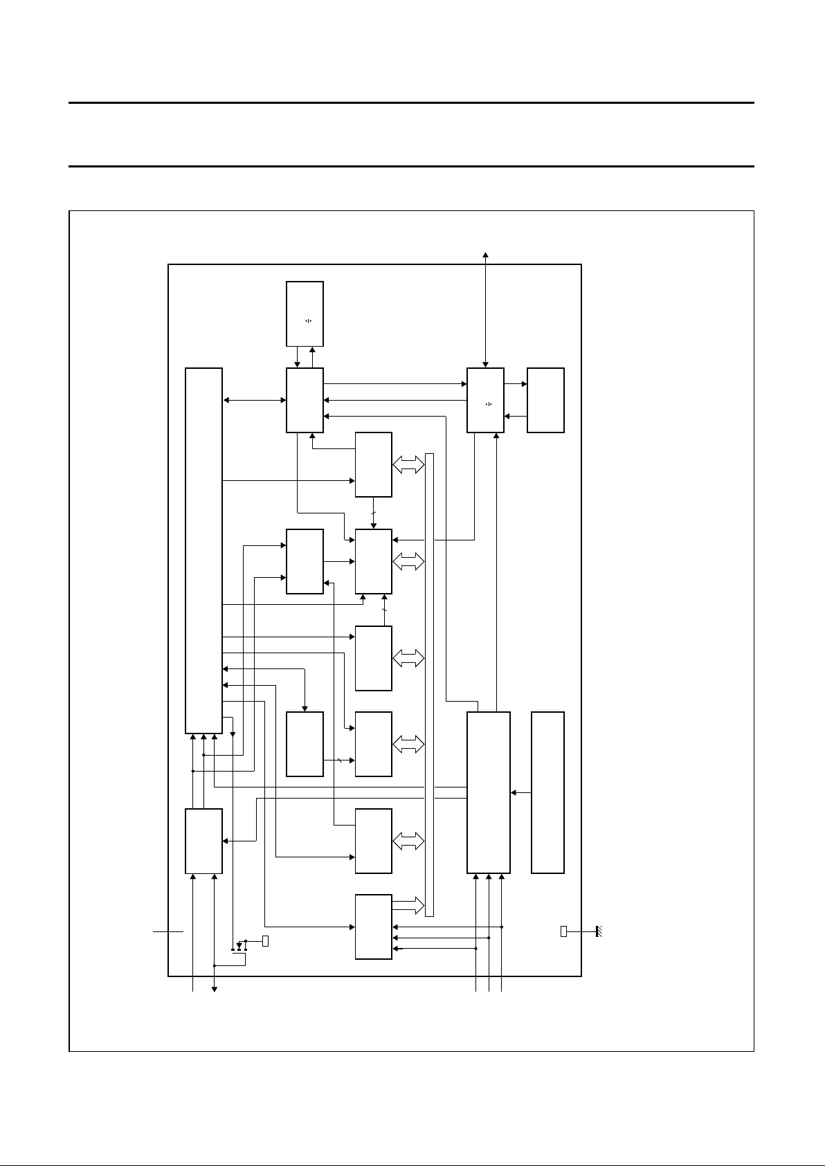
6 BLOCK DIAGRAM
handbook, full pagewidth
MGD927
TEST MODE DECODER
POWER-ON-RESET
I
2
C-BUS CONTROL LOGIC
SEQUENCER
ADDRESS
HIGH
REGISTER
BYTE
COUNTER
DIVIDER
( 128)
EE
CONTROL
TIMER
( 16)
EEPROM
ADDRESS
POINTER
BYTE
LATCH
(8 bytes)
SHIFT
REGISTER
ADDRESS
SWITCH
INPUT
FILTER
OSCILLATOR
8
4
3
n
7
PTC
PCF85xxC-2
4
V
SS
A1
A2
A0
321
8
V
DD
6
5
SCL
SDA
Fig.1 Block diagram.
The pin numbers in this block diagram refer to the PCF8582C-2.
For PCF8594C-2 and PCF8598C-2 please see Chapter 7.

1997 Feb 13 6
Philips Semiconductors Product specification
256 to 1024 × 8-bit CMOS EEPROMs with
I
2
C-bus interface
PCF85xxC-2 family
7 PINNING
7.1 Pin description PCF8582C-2
SYMBOL PIN DESCRIPTION
A0 1 address input 0
A1 2 address input 1
A2 3 address input 2
V
SS
4 negative supply voltage
SDA 5 serial data input/output (I
2
C-bus)
SCL 6 serial clock input (I
2
C-bus)
PTC 7 programming time control output
V
DD
8 positive supply voltage
Fig.2 Pin configuration PCF8582C-2.
handbook, halfpage
1
2
3
4
8
7
6
5
A0
A1
A2
V
SS
SDA
SCL
PTC
V
DD
PCF8582C-2
MGD928
7.2 Pin description PCF8594C-2
SYMBOL PIN DESCRIPTION
WP 1 write-protection input
A1 2 address input 1
A2 3 address input 2
V
SS
4 negative supply voltage
SDA 5 serial data input/output (I
2
C-bus)
SCL 6 serial clock input (I
2
C-bus)
PTC 7 programming time control output
V
DD
8 positive supply voltage
Fig.3 Pin configuration PCF8594C-2.
handbook, 2 columns
1
2
3
4
8
7
6
5
WP
A1
A2
V
SS
SDA
SCL
PTC
V
DD
PCF8594C-2
MGL001
7.3 Pin description PCF8598C-2
SYMBOL PIN DESCRIPTION
WP 1 write-protection input
n.c. 2 not connected
A2 3 address input 2
V
SS
4 negative supply voltage
SDA 5 serial data input/output (I
2
C-bus)
SCL 6 serial clock input (I
2
C-bus)
PTC 7 programming time control output
V
DD
8 positive supply voltage
Fig.4 Pin configuration PCF8598C-2.
handbook, halfpage
1
2
3
4
8
7
6
5
WP
n.c.
A2
V
SS
SDA
SCL
PTC
V
DD
PCF8598C-2
MGL002

1997 Feb 13 7
Philips Semiconductors Product specification
256 to 1024 × 8-bit CMOS EEPROMs with
I
2
C-bus interface
PCF85xxC-2 family
8I2C-BUS PROTOCOL
The I2C-bus is for 2-way, 2-line communication between
different ICs or modules. The serial bus consists of two
bidirectional lines: one for data signals (SDA), and one for
clock signals (SCL).
Both the SDA and SCL lines must be connected to a
positive supply voltage via a pull-up resistor.
The following protocol has been defined:
• Data transfer may be initiated only when the bus is not
busy.
• During data transfer, the data line must remain stable
whenever the clock line is HIGH. Changes in the data
line while the clock line is HIGH will be interpreted as
control signals.
8.1 Bus conditions
The following bus conditions have been defined:
• Bus not busy: both data and clock lines remain HIGH.
• Start data transfer: a change in the state of the data
line, from HIGH-to-LOW, while the clock is HIGH,
defines the START condition.
• Stop data transfer: a change in the state of the data
line, from LOW-to-HIGH, while the clock is HIGH,
defines the STOP condition.
• Data valid: the state of the data line represents valid
data when, after a START condition, the data line is
stable for the duration of the HIGH period of the clock
signal. There is one clock pulse per bit of data.
8.2 Data transfer
Each data transfer is initiated with a START condition and
terminated with a STOP condition. The number of the data
bytes, transferred between the START and STOP
conditions is limited to 7 bytes in the E/W mode and
8 bytes in the page E/W mode.
Data transfer is unlimited in the read mode.
The information is transmitted in bytes and each receiver
acknowledges with a ninth bit.
Within the I
2
C-bus specifications a low-speed mode (2 kHz
clock rate) and a high speed mode (100 kHz clock rate)
are defined. The PCF85xxC-2 operates in both modes.
By definition a device that sends a signal is called a
‘transmitter’, and the device which receives the signal is
called a ‘receiver’. The device which controls the signal is
called the ‘master’. The devices that are controlled by the
master are called ‘slaves’.
Each byte is followed by one acknowledge bit. This
acknowledge bit is a HIGH level, put on the bus by the
transmitter. The master generates an extra acknowledge
related clock pulse. The slave receiver which is addressed
is obliged to generate an acknowledge after the reception
of each byte.
The master receiver must generate an acknowledge after
the reception of each byte that has been clocked out of the
slave transmitter.
The device that acknowledges has to pull down the SDA
line during the acknowledge clock pulse in such a way that
the SDA line is stable LOW during the HIGH period of the
acknowledge related clock pulse.
Set-up and hold times must be taken into account.
A master receiver must signal an end of data to the slave
transmitter by not generating an acknowledge on the last
byte that has been clocked out of the slave. In this event
the transmitter must leave the data line HIGH to enable the
master generation of the STOP condition.
1997 Feb 13 8
Philips Semiconductors Product specification
256 to 1024 × 8-bit CMOS EEPROMs with
I
2
C-bus interface
PCF85xxC-2 family
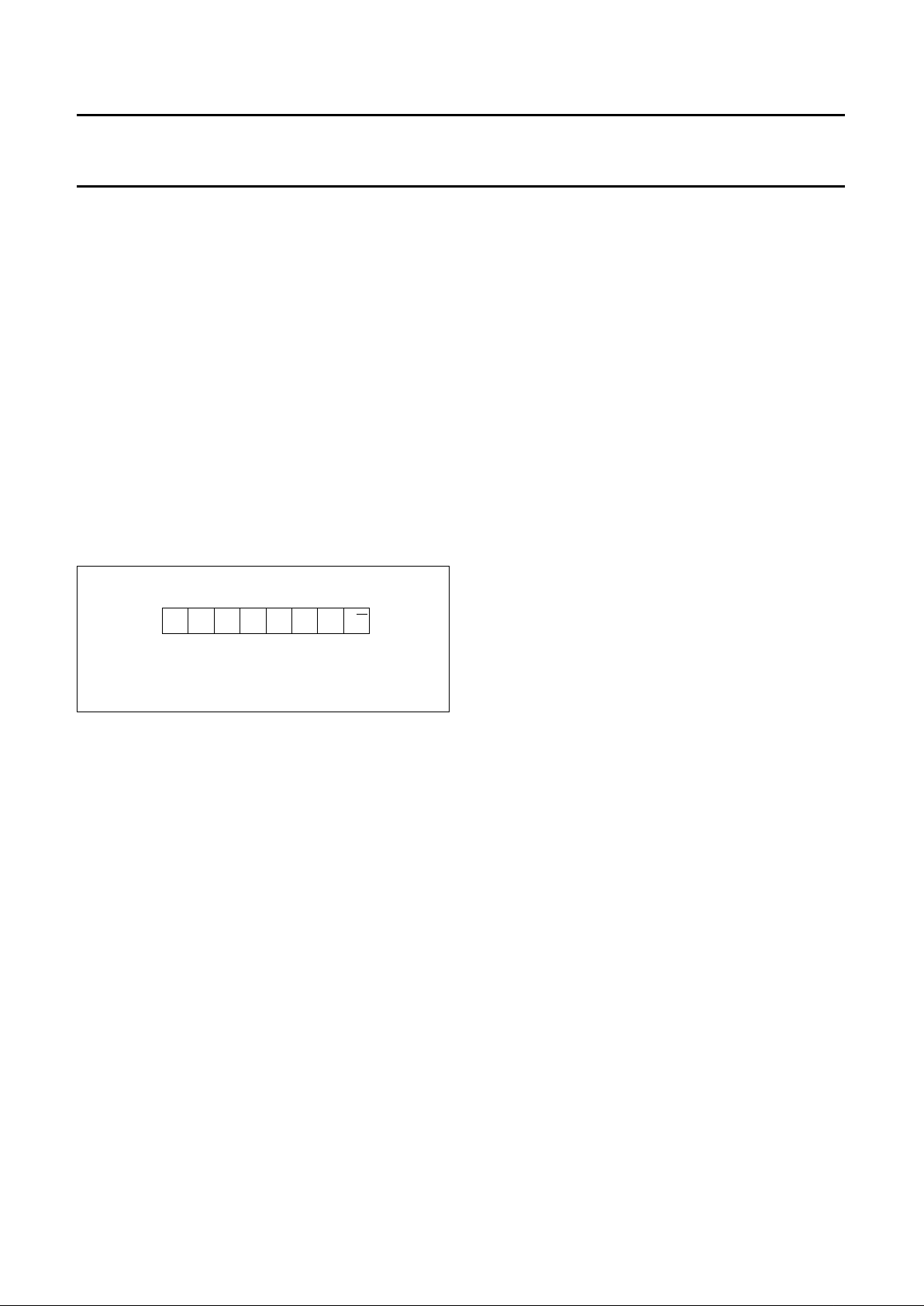
8.3 Device addressing
Following a START condition the bus master must output
the address of the slave it is accessing. The 4 MSBs of the
slave address are the device type identifier (see Fig.5).
For the PCF85xxC-2 this is fixed to ‘1010’.
The next three significant bits address a particular device
or memory page (page = 256 bytes of memory). A system
could have up to eight PCF8582C-2 (or four PCF8594C-2
containing two memory pages each or two PCF8598C-2
containing four memory pages each, respectively) devices
on the bus. The eight addresses are defined by the state
of the A0, A1 and A2 inputs.
The last bit of the slave address defines the operation to
be performed. When set to logic 1 a read operation is
selected.
Address bits must be connected to either V
DD
or VSS.
8.4 Write operations
8.4.1 BYTE/WORD WRITE
For a write operation the PCF85xxC-2 requires a second
address field. This address field is a word address
providing access to the 256 words of memory. Upon
receipt of the word address the PCF85xxC-2 responds
with an acknowledge and awaits the next eight bits of data,
again responding with an acknowledge. Word address is
automatically incremented. The master can now terminate
the transfer by generating a STOP condition or transmit up
to six more bytes of data and then terminate by generating
a STOP condition.
Fig.5 Slave address.
handbook, halfpage
MBC793
1010A2A1A0R/W
After this STOP condition the E/W cycle starts and the bus
is free for another transmission. Its duration is 10 ms per
byte.
During the E/W cycle the slave receiver does not send an
acknowledge bit if addressed via the I2C-bus.
8.4.2 P
AGE WRITE
The PCF85xxC-2 is capable of an eight-byte page write
operation. It is initiated in the same manner as the byte
write operation. The master can transmit eight data bytes
within one transmission. After receipt of each byte the
PCF85xxC-2 will respond with an acknowledge.
The typical E/W time in this mode is 9 × 3.5 ms = 31.5 ms.
Erasing a block of 8 bytes in page mode takes typical
3.5 ms and sequential writing of these 8 bytes another
typical 28 ms.
After the receipt of each data byte the three low order bits
of the word address are internally incremented. The high
order five bits of the address remain unchanged. The slave
acknowledges the reception of each data byte with an
ACK. The I
2
C-bus data transfer is terminated by the
master after the 8th byte with a STOP condition. If the
master transmits more than eight bytes prior to generating
the STOP condition, no acknowledge will be given on the
ninth (and following) data bytes and the whole
transmission will be ignored and no programming will be
done. As in the byte write operation, all inputs are disabled
until completion of the internal write cycles.
8.4.3 R
EMARK
A write to the EEPROM is always performed if the pin WP
is LOW (not on PCF8582C-2). If WP is HIGH, then the
upper half of the EEPROM is write-protected and no
acknowledge will be given by the PCF85xxC-2 when one
of the upper 256 EEPROM bytes (PCF8594C-2) or
512 EEPROM bytes (PCF8598C-2) is addressed.
However, an acknowledge will be given after the slave
address and the word address.
 Loading...