

Philips PCF8593P, PCF8593T Datasheet

INTEGRATED CIRCUITS
DATA SH EET
PCF8593
Low power clock/calendar
Product specification
Supersedes data of July 1994
File under Integrated Circuits, IC12
1997 Mar 25

Philips Semiconductors Product specification
Low power clock/calendar PCF8593
CONTENTS
1 FEATURES
2 GENERAL DESCRIPTION
3 QUICK REFERENCE DATA
4 ORDERING INFORMATION
5 BLOCK DIAGRAM
6 PINNING
7 FUNCTIONAL DESCRIPTION
7.1 Counter function modes
7.2 Alarm function modes
7.3 Control/status register
7.4 Counter registers
7.5 Alarm control register
7.6 Alarm registers
7.7 Timer
7.8 Event counter mode
7.9 Interrupt output
7.10 Oscillator and divider
7.10.1 Designing
7.11 Initialization (see Fig.12)
8 CHARACTERISTICS OF THE I2C-BUS
8.1 Bit transfer
8.2 Start and stop conditions
8.3 System configuration
8.4 Acknowledge
9I
9.1 Addressing
9.2 Clock/calendar READ/WRITE cycles
2
C-BUS PROTOCOL
10 LIMITING VALUES
11 HANDLING
12 DC CHARACTERISTICS
13 AC CHARACTERISTICS
14 APPLICATION INFORMATION
14.1 Quartz frequency adjustment
14.1.1 Method 1: Fixed OSCI capacitor
14.1.2 Method 2: OSCI Trimmer
14.1.3 Method 3: direct output
15 PACKAGE OUTLINES
16 SOLDERING
16.1 Introduction
16.2 DIP
16.2.1 Soldering by dipping or by wave
16.2.2 Repairing soldered joints
16.3 SO
16.3.1 Reflow soldering
16.3.2 Wave soldering
16.3.3 Repairing soldered joints
17 DEFINITIONS
18 LIFE SUPPORT APPLICATIONS
19 PURCHASE OF PHILIPS I2C COMPONENTS
1997 Mar 25 2

Philips Semiconductors Product specification
Low power clock/calendar PCF8593
1 FEATURES
• I2C-bus interface operating supply voltage: 2.5 to 6.0 V
• Clock operating supply voltage (T
=0to+70°C):
amb
1.0 to 6.0 V
• 8 bytes scratchpad RAM (when alarm not used)
• Data retention voltage: 1.0 to 6.0 V
• External RESET input resets I2C interface (only)
• Operating current (f
= 0 Hz, 32 kHz time base,
scl
VDD= 2.0 V): typ. 1 µA
• Clock function with four year calendar
• Universal timer with alarm and overflow indication
• 24 or 12 hour format
• 32.768 kHz or 50 Hz time base
2
• Serial input/output bus (I
C-bus)
• Automatic word address incrementing
• Programmable alarm, timer and interrupt function
• Space-saving SO8 package available
• Slave address:
– READ A3
– WRITE A2.
2 GENERAL DESCRIPTION
The PCF8593 is a CMOS clock/calendar circuit, optimized
for low power consumption. Addresses and data are
transferred serially via the two-line bidirectional I
2
C-bus.
The built-in word address register is incremented
automatically after each written or read data byte.
The built-in 32.768 kHz oscillator circuit and the first 8
bytes of RAM are used for the clock/calendar and counter
functions. The next 8 bytes may be programmed as alarm
registers or used as free RAM space.
3 QUICK REFERENCE DATA
SYMBOL PARAMETER CONDITIONS MIN. TYP. MAX. UNIT
V
DD
I
DD
I
DD
T
amb
T
stg
supply voltage operating mode I2C-bus active 2.5 − 6.0 V
2
C-bus inactive 1.0 − 6.0 V
I
supply current operating mode f
supply current clock mode f
= 100 kHz −−200 µA
scl
= 0 Hz; VDD=5V − 4.0 15.0 µA
scl
= 0 Hz; VDD=2V − 1.0 8.0 µA
f
scl
operating ambient temperature −40 − +85 °C
storage temperature −65 − +150 °C
4 ORDERING INFORMATION
TYPE
NUMBER
NAME DESCRIPTION VERSION
PACKAGE
PCF8593P DIP8 plastic dual in-line package; 8 leads (300 mil) SOT97-1
PCF8593T SO8 plastic small outline package; 8leads; body width 3.9mm SOT96-1
1997 Mar 25 3
Philips Semiconductors Product specification
Low power clock/calendar PCF8593
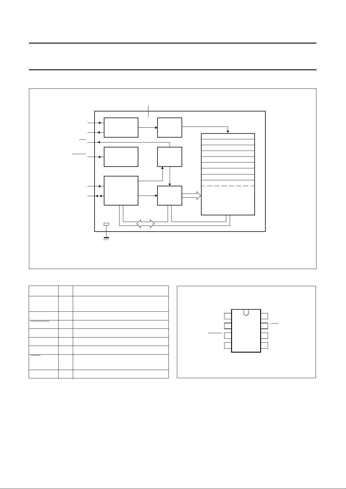
5 BLOCK DIAGRAM
handbook, full pagewidth
OSCI
OSCO
INT
RESET
SCL
SDA
1
2
7
3
6
5
V
SS
OSCILLATOR
32.768 kHz
RESET
2
I C-BUS
INTERFACE
4
V
DD
8
DIVIDER
1 : 256
100 : 128
CONTROL
LOGIC
100 Hz
PCF8593
ADDRESS
REGISTER
Fig.1 Block diagram.
control/status
hundredths of a second
seconds
minutes
hours
year/date
weekdays/months
timer
alarm control
alarm registers
or RAM
00
01
07
08
0F
MBD808
6 PINNING
SYMBOL PIN DESCRIPTION
OSCI 1 oscillator input, 50 Hz or event-pulse
input
OSCO 2 oscillator output
RESET 3 reset input (active LOW)
V
SS
4 negative supply
SDA 5 serial data input/output
SCL 6 serial clock input
INT 7 open drain interrupt output
(active LOW)
V
DD
8 positive supply
1
OSCI
2
OSCO
RESET
V
SS
3
4
PCF8593P
PCF8593T
MBD809
Fig.2 Pin configuration.
V
8
DD
7
INT
SCL
6
SDA
5
1997 Mar 25 4

Philips Semiconductors Product specification
Low power clock/calendar PCF8593
7 FUNCTIONAL DESCRIPTION
The PCF8593 contains sixteen 8-bit registers with an 8-bit
auto-incrementing address register, an on-chip
32.768 kHz oscillator circuit, a frequency divider and a
serial two-line bidirectional I2C-bus interface.
The first 8 registers (memory addresses 00 to 07) are
designed as addressable 8-bit parallel registers. The first
register (memory address 00) is used as a control/status
register. The memory addresses 01 to 07 are used as
counters for the clock function. The memory addresses
08 to 0F may be programmed as alarm registers or used
as free RAM locations.
7.1 Counter function modes
When the control/status register is programmed, a
32.768 kHz clock mode, a 50 Hz clock mode or an
event-counter mode can be selected.
In the clock modes the hundredths of a second, seconds,
minutes, hours, date, month (four year calendar) and
weekday are stored in a BCD format. The timer register
stores up to 99 days. The event counter mode is used to
count pulses applied to the oscillator input (OSCO left
open-circuit). The event counter stores up to 6 digits of
data.
When one of the counters is read (memory locations
01 to 07), the contents of all counters are strobed into
capture latches at the beginning of a read cycle. Therefore,
faulty reading of the count during a carry condition is
prevented.
When a counter is written, other counters are not affected.
7.2 Alarm function modes
By setting the alarm enable bit of the control/status register
the alarm control register (address 08) is activated.
By setting the alarm control register a dated alarm, a daily
alarm, a weekday alarm or a timer alarm may be
programmed. In the clock modes, the timer register
(address 07) may be programmed to count hundredths of
a second, seconds, minutes, hours or days. Days are
counted when an alarm is not programmed.
Whenever an alarm event occurs the alarm flag of the
control/status register is set. A timer alarm event will set
the alarm flag and an overflow condition of the timer will set
the timer flag. The open-drain interrupt output is switched
on (active LOW) when the alarm or timer flag is set
(enabled). The flags remain set until directly reset by a
write operation.
When the alarm is disabled (Bit 2 of control/status
register = 0) the alarm registers at addresses 08 to 0F may
be used as free RAM.
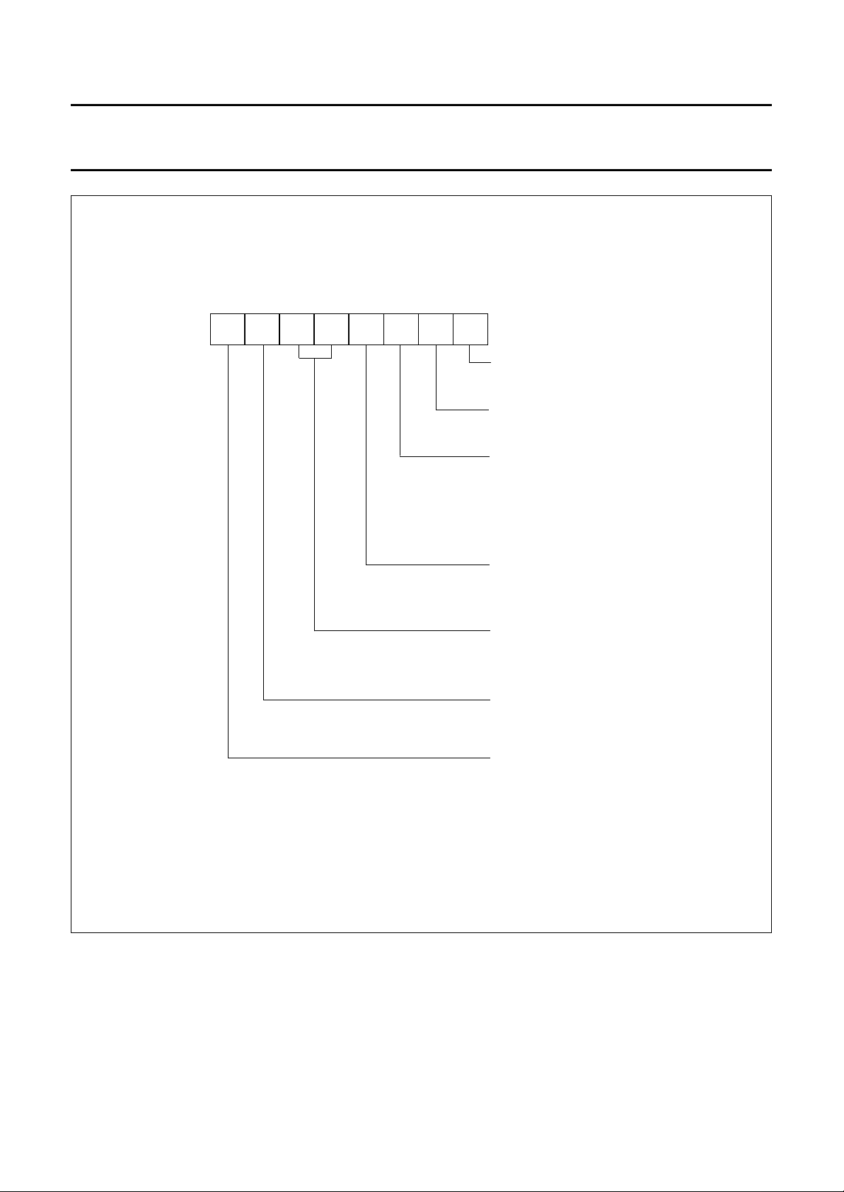
7.3 Control/status register
The control/status register is defined as the memory
location 00 with free access for reading and writing via the
2
C-bus. All functions and options are controlled by the
I
contents of the control/status register (see Fig.3).
7.4 Counter registers
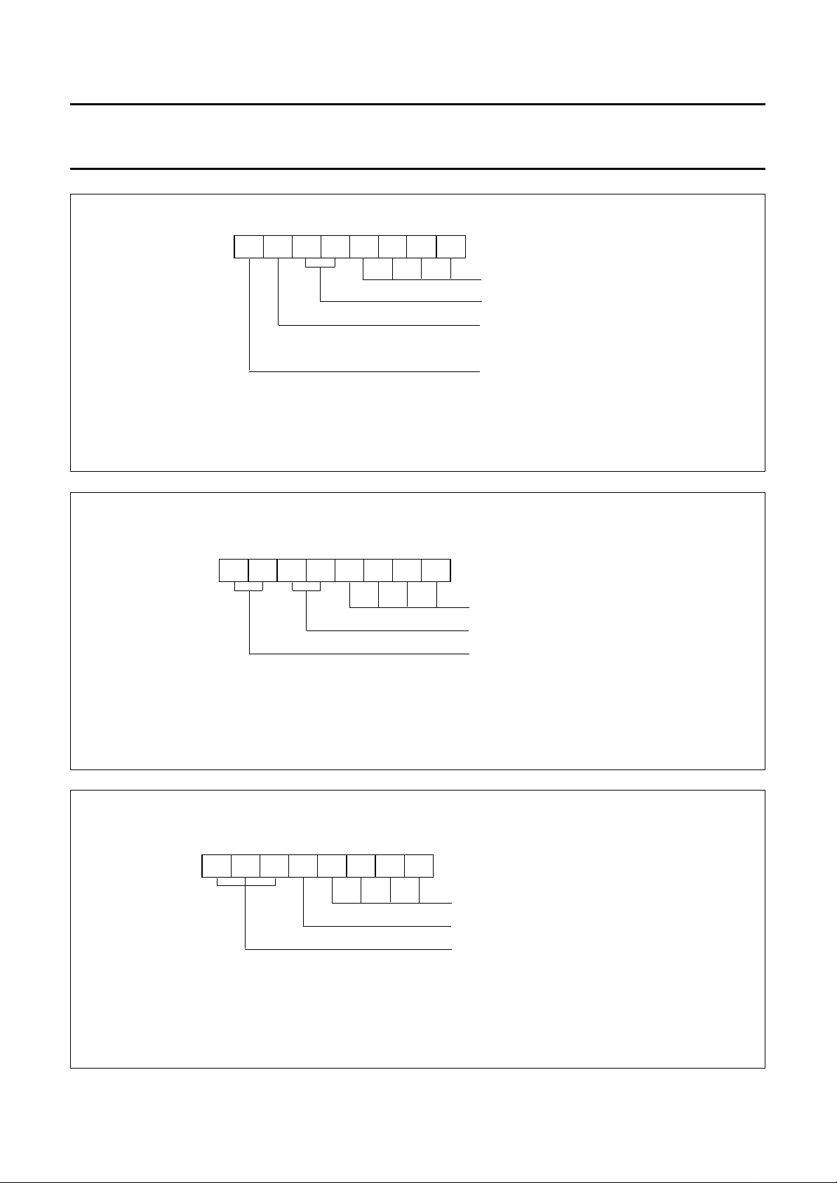
In the clock modes 24 h or 12 h format can be selected by
setting the most significant bit of the hours counter
register. The format of the hours counter is shown in Fig.5.
The year and date are packed into memory location 05
(see Fig 6). The weekdays and months are packed into
memory location 06 (see Fig.7). When reading these
memory locations the year and weekdays are masked out
when the mask flag of the control/status register is set.
This allows the user to read the date and month count
directly.
In the event-counter mode events are stored in BCD
format. D5 is the most significant and D0 the least
significant digit. The divider is by-passed.
In the different modes the counter registers are
programmed and arranged as shown in Fig.4. Counter
cycles are listed in Table 1.
1997 Mar 25 5
Philips Semiconductors Product specification
Low power clock/calendar PCF8593
handbook, full pagewidth
MSB LSB
76543210
MBD810
memory location 00
timer flag (50% duty factor
seconds flag if alarm
enable bit is 0)
alarm flag (50% duty factor
minutes flag if alarm
enable bit is 0)
alarm enable bit:
0 alarm disabled: flags toggle
alarm control register disabled
(memory locations 08 to 0F
can be treated as RAM)
1 enable Alarm Control register
(memory location 08 is the
Alarm Control register)
mask flag:
0 read locations 05 to 06
unmasked
1 read date and month count
directly
function mode :
00 clock mode 32.768 kHz
01 clock mode 50 Hz
10 event-counter mode
11 test modes
hold last count flag :
0 count
1 store and hold last count in
capture latches
stop counting flag :
0 count pulses
1 stop counting, reset divider
Fig.3 Control/status register.
1997 Mar 25 6
Philips Semiconductors Product specification
Low power clock/calendar PCF8593
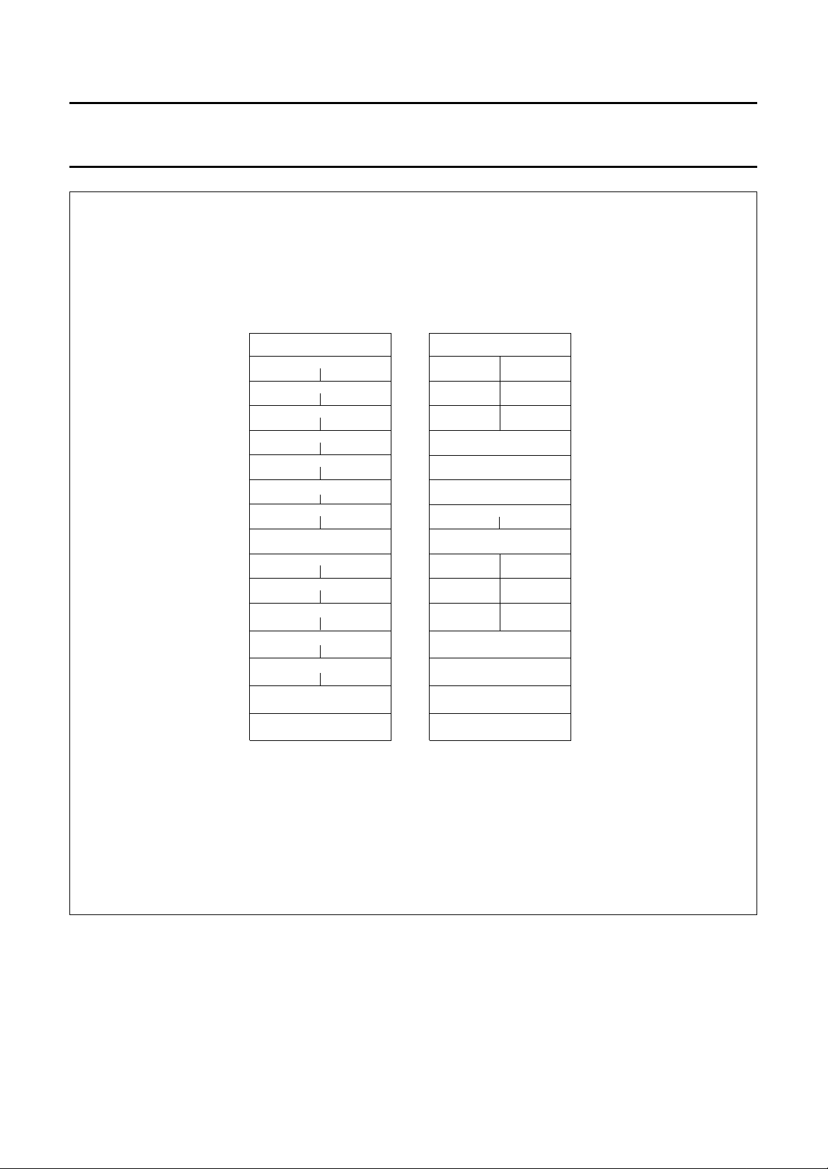
handbook, full pagewidth
control/status
hundredths of a second
1/10 s
10 s
10 min
10 h
10 day
weekday/month
10 month
10 day
alarm control
hundredths of a second
1/10 s 1/100 s
alarm seconds
alarm minutes
alarm hours
alarm month
alarm timer
1/100 s
seconds
1 s
minutes
1 min
hours
1 h
year/date
1 day
1 month
timer
1 day
alarm date
control/status
D1
D3
D5
T1
alarm control
alarm alarm
D1
D3
D5
alarm timer
free
free
free
timer
free
free
free
D0
D2
D4
T0
D0
D2
D4
00
01
02
03
04
05
06
07
08
09
0A
0B
0C
0D
0E
0F
CLOCK MODES EVENT COUNTER
Fig.4 Register arrangement.
1997 Mar 25 7
MBD811
Philips Semiconductors Product specification
Low power clock/calendar PCF8593
handbook, full pagewidth
handbook, full pagewidth
MSB LSB
76543210
MBD812
Fig.5 Format of the hours counter.
MSB LSB
76543210
MBD813
memory location 04 (hours counter)
unit hours BCD
ten hours (0 to 12 binary)
AM/PM flag:
0 AM
1 PM
format:
0 24 h format, AM/PM flag
remains unchanged
1 12 h format, AM/PM flag
will be updated
memory location 05 (year/date)
unit hours BCD
ten days (0 to 3 binary)
year (0 to 3 binary, read as 0 if
the mask flag is set)
Fig.6 Format of the year/date counter.
handbook, full pagewidth
MSB LSB
76543210
MBD814
Fig.7 Format of the weekdays/months counter.
1997 Mar 25 8
memory location 06 (weekdays/months)
unit months BCD
ten months
weekdays (0 to 6 binary, read as 0 if
the mask flag is set)

Philips Semiconductors Product specification
Low power clock/calendar PCF8593
Table 1 Cycle length of the time counters, clock modes.
UNIT COUNTING CYCLE CARRY TO NEXT UNIT
Hundredths of a second 00 to 99 99 to 00 −
Seconds 00 to 59 59 to 00 −
Minutes 00 to 59 59 to 00 −
Hours (24 h) 00 to 23 23 to 00 −
Hours (12 h) 12 AM −−
01 AM to 11AM −−
12 PM −−
01 PM to 11PM 11 PM to 12 AM −
Date 01 to 31 31 to 01 1, 3, 5, 7, 8, 10 and 12
01 to 30 30 to 01 4, 6, 9 and 11
01 to 29 29 to 01 2, year = 0
01 to 28 28 to 01 2, year = 1, 2 and 3
Months 01 to 12 12 to 01 −
Year 0 to 3 −−
Weekdays 0 to 6 6 to 0 −
Timer 00 to 99 no carry −
7.5 Alarm control register
When the alarm enable bit of the control/status register is
set (address 00, bit 2) the alarm control register
(address 08) is activated. All alarm, timer, and interrupt
output functions are controlled by the contents of the alarm
control register (see Fig.8).
An alarm signal is generated when the contents of the
alarm registers matches bit-by-bit the contents of the
involved counter registers. The year and weekday bits are
ignored in a dated alarm. A daily alarm ignores the month
and date bits. When a weekday alarm is selected, the
contents of the alarm weekday/month register will select
the weekdays on which an alarm is activated (see Fig.9).
CONTENTS OF THE
MONTH COUNTER
7.6 Alarm registers
All alarm registers are allocated with a constant address
offset of hexadecimal 08 to the corresponding counter
registers (see Fig.4,Register arrangement).
1997 Mar 25 9
Remark: in the 12 h mode, bits 6 and 7 of the alarm hours
register must be the same as the hours counter.
 Loading...