

Philips pcf8591 DATASHEETS
INTEGRATED CIRCUITS
DATA SH EET
PCF8591
8-bit A/D and D/A converter
Product specification
Supersedes data of 1997 Apr 02
File under Integrated Circuits, IC12
1998 Jul 02

Philips Semiconductors Product specification
8-bit A/D and D/A converter PCF8591
CONTENTS
1 FEATURES
2 APPLICATIONS
3 GENERAL DESCRIPTION
4 ORDERING INFORMATION
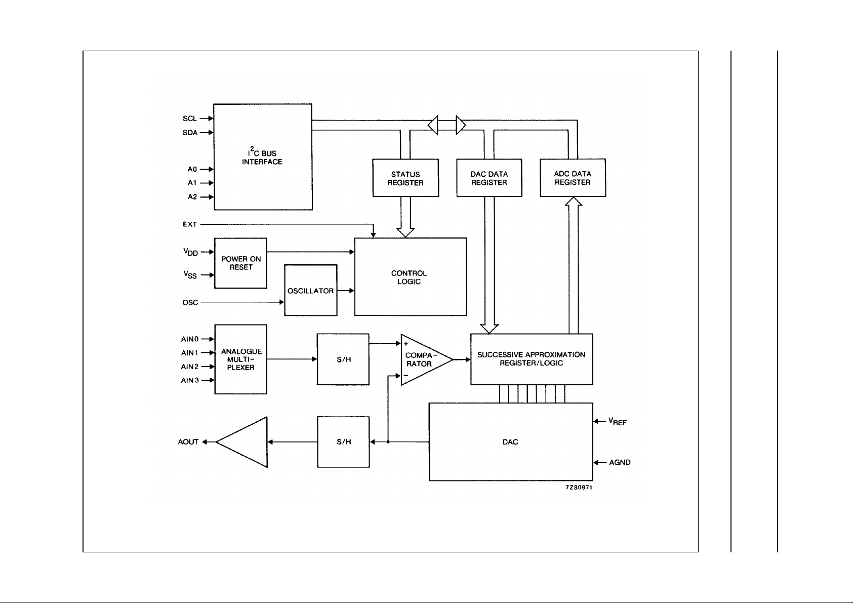
5 BLOCK DIAGRAM
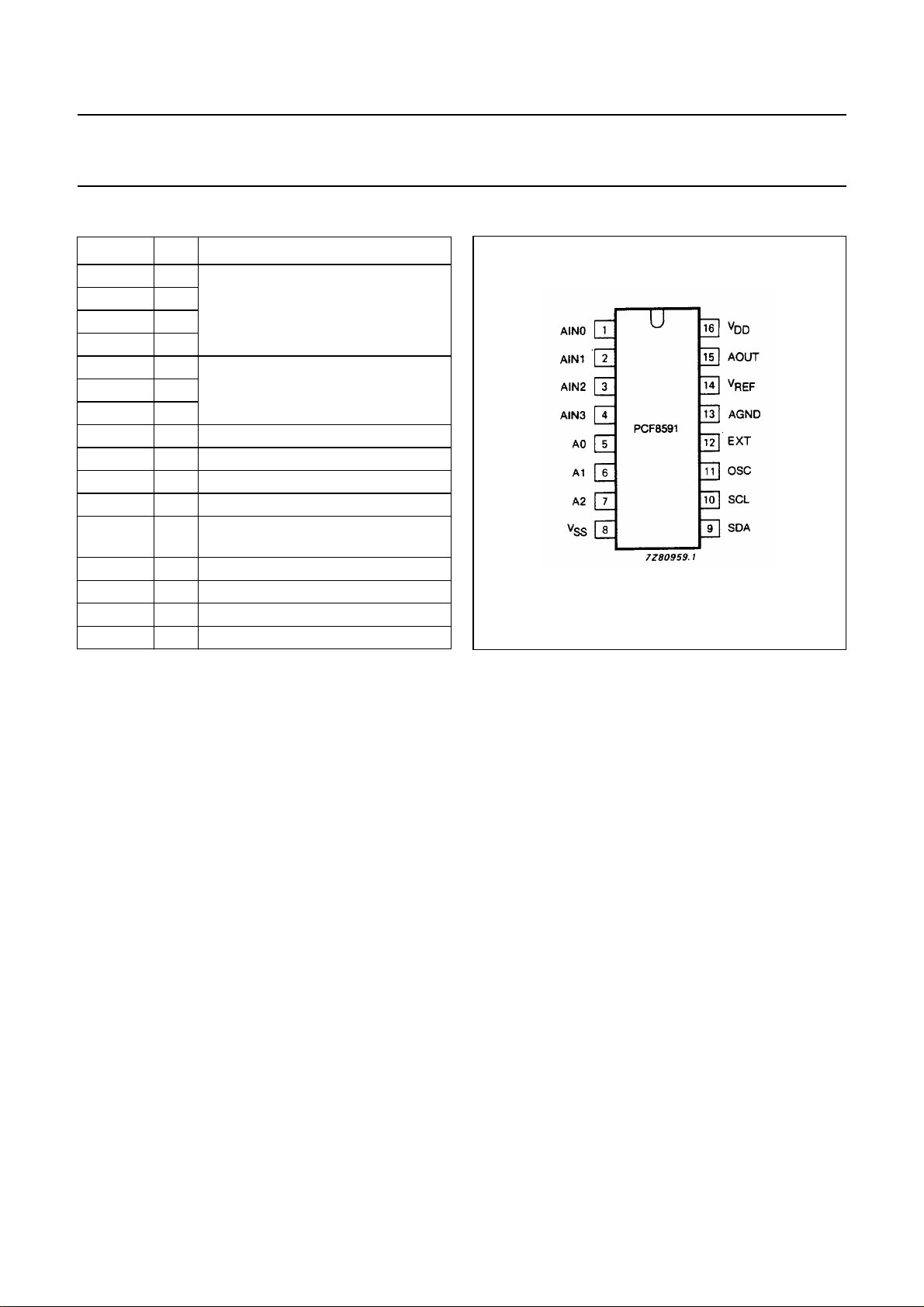
6 PINNING
7 FUNCTIONAL DESCRIPTION
7.1 Addressing
7.2 Control byte
7.3 D/A conversion
7.4 A/D conversion
7.5 Reference voltage
7.6 Oscillator
8 CHARACTERISTICS OF THE I2C-BUS
8.1 Bit transfer
8.2 Start and stop conditions
8.3 System configuration
8.4 Acknowledge
8.5 I2C-bus protocol
9 LIMITING VALUES
10 HANDLING
11 DC CHARACTERISTICS
12 D/A CHARACTERISTICS
13 A/D CHARACTERISTICS
14 AC CHARACTERISTICS
15 APPLICATION INFORMATION
16 PACKAGE OUTLINES
17 SOLDERING
17.1 Introduction
17.2 DIP
17.2.1 Soldering by dipping or by wave
17.2.2 Repairing soldered joints
17.3 SO
17.3.1 Reflow soldering
17.3.2 Wave soldering
17.3.3 Repairing soldered joints
18 DEFINITIONS
19 LIFE SUPPORT APPLICATIONS
20 PURCHASE OF PHILIPS I2C COMPONENTS
1998 Jul 02 2
Philips Semiconductors Product specification
8-bit A/D and D/A converter PCF8591
1 FEATURES
• Single power supply
• Operating supply voltage 2.5 V to 6 V
• Low standby current
• Serial input/output via I2C-bus
• Address by 3 hardware address pins
• Sampling rate given by I2C-bus speed
• 4 analog inputs programmable as single-ended or
differential inputs
• Auto-incremented channel selection
• Analog voltage range from V
SS
to V
DD
• On-chip track and hold circuit
• 8-bit successive approximation A/D conversion
• Multiplying DAC with one analog output.
2 APPLICATIONS
• Closed loop control systems
• Low power converter for remote data acquisition
• Battery operated equipment
• Acquisition of analog values in automotive, audio and
TV applications.
3 GENERAL DESCRIPTION
The PCF8591 is a single-chip, single-supply low power
8-bit CMOS data acquisition device with four analog
2
inputs, one analog output and a serial I
C-bus interface.
Three address pins A0, A1 and A2 are used for
programming the hardware address, allowing the use of
up to eight devices connected to the I2C-bus without
additional hardware. Address, control and data to and from
the device are transferred serially via the two-line
bidirectional I2C-bus.
The functions of the device include analog input
multiplexing, on-chip track and hold function, 8-bit
analog-to-digital conversion and an 8-bit digital-to-analog
conversion. The maximum conversion rate is given by the
2
maximum speed of the I
C-bus.
4 ORDERING INFORMATION
TYPE
NUMBER
NAME DESCRIPTION VERSION
PACKAGE
PCA8591P DIP16 plastic dual in-line package; 16 leads (300 mil); long body SOT38-1
PCA8591T SO16 plastic small outline package; 16 leads; body width 7.5 mm SOT162-1
1998 Jul 02 3
This text is here in white to force landscape pages to be rotated correctly when browsing through the pdf in the Acrobat reader.This text is here in
_white to force landscape pages to be rotated correctly when browsing through the pdf in the Acrobat reader.This text is here inThis text is here in
white to force landscape pages to be rotated correctly when browsing through the pdf in the Acrobat reader. white to force landscape pages to be ...
1998 Jul 02 4
5 BLOCK DIAGRAM
8-bit A/D and D/A converter PCF8591
Philips Semiconductors Product specification
Fig.1 Block diagram.
Philips Semiconductors Product specification
8-bit A/D and D/A converter PCF8591
6 PINNING
SYMBOL PIN DESCRIPTION
AINO 1
AIN1 2
AIN2 3
AIN3 4
A0 5
A2 7
V
SS
SDA 9 I
SCL 10 I
OSC 11 oscillator input/output
EXT 12 external/internal switch for oscillator
AGND 13 analog ground
V
REF
AOUT 15 analog output (D/A converter)
V
DD
analog inputs
(A/D converter)
hardware addressA1 6
8 negative supply voltage
2
C-bus data input/output
2
C-bus clock input
input
14 voltage reference input
16 positive supply voltage
Fig.2 Pinning diagram.
1998 Jul 02 5
Philips Semiconductors Product specification
8-bit A/D and D/A converter PCF8591
7 FUNCTIONAL DESCRIPTION
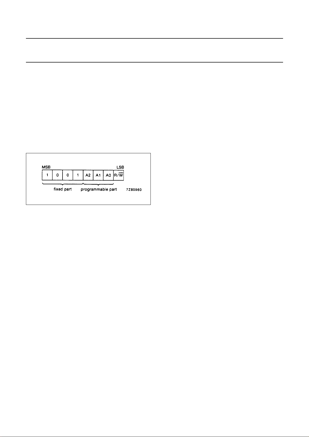
7.1 Addressing
Each PCF8591 device in an I
sending a valid address to the device. The address
consists of a fixed part and a programmable part.
The programmable part must be set according to the
address pins A0, A1 and A2. The address always has to
be sent as the first byte after the start condition in the
I2C-bus protocol. The last bit of the address byte is the
read/write-bit which sets the direction of the following data
transfer (see Figs 3, 15 and 16).
Fig.3 Address byte.
2
C-bus system is activated by
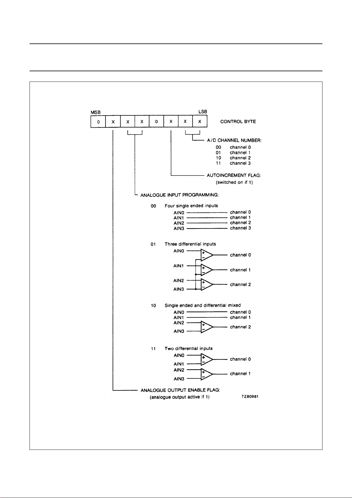
7.2 Control byte
The second byte sent to a PCF8591 device will be stored
in its control register and is required to control the device
function.
The upper nibble of the control register is used for enabling
the analog output, and for programming the analog inputs
as single-ended or differential inputs. The lower nibble
selects one of the analog input channels defined by the
upper nibble (see Fig.4). If the auto-increment flag is set
the channel number is incremented automatically after
each A/D conversion.
If the auto-increment mode is desired in applications
where the internal oscillator is used, the analog output
enable flag in the control byte (bit 6) should be set. This
allows the internal oscillator to run continuously, thereby
preventing conversion errors resulting from oscillator
start-up delay. The analog output enable flag may be reset
at other times to reduce quiescent power consumption.
The selection of a non-existing input channel results in the
highest available channel number being allocated.
Therefore, if the auto-increment flag is set, the next
selected channel will be always channel 0. The most
significant bits of both nibbles are reserved for future
functions and have to be set to 0. After a Power-on reset
condition all bits of the control register are reset to 0.
The D/A converter and the oscillator are disabled for power
saving. The analog output is switched to a high-impedance
state.
1998 Jul 02 6
Philips Semiconductors Product specification
8-bit A/D and D/A converter PCF8591
Fig.4 Control byte.
1998 Jul 02 7

Philips Semiconductors Product specification
8-bit A/D and D/A converter PCF8591
7.3 D/A conversion
The third byte sent to a PCF8591 device is stored in the
DAC data register and is converted to the corresponding
analog voltage using the on-chip D/A converter. This D/A
converter consists of a resistor divider chain connected to
the external reference voltage with 256 taps and selection
switches. The tap-decoder switches one of these taps to
the DAC output line (see Fig.5).
The analog output voltage is buffered by an auto-zeroed
unity gain amplifier. This buffer amplifier may be switched
on or off by setting the analog output enable flag of the
control register. In the active state the output voltage is
held until a further data byte is sent.
The on-chip D/A converter is also used for successive
approximation A/D conversion. In order to release the
DAC for an A/D conversion cycle the unity gain amplifier is
equipped with a track and hold circuit. This circuit holds the
output voltage while executing the A/D conversion.
The output voltage supplied to the analog output AOUT is
given by the formula shown in Fig.6. The waveforms of a
D/A conversion sequence are shown in Fig.7.
Fig.5 DAC resistor divider chain.
1998 Jul 02 8

Philips Semiconductors Product specification
8-bit A/D and D/A converter PCF8591
Fig.6 DAC data and DC conversion characteristics.
Fig.7 D/A conversion sequence.
1998 Jul 02 9
 Loading...