

Philips pcf8575 DATASHEETS
INTEGRATED CIRCUITS
DATA SH EET
PCF8575
Remote 16-bit I/O expander for
2
I
C-bus
Product specification
Supersedes data of 1999 Feb 25
File under Integrated Circuits, IC12
1999 Apr 07

Philips Semiconductors Product specification
Remote 16-bit I/O expander for I2C-bus
CONTENTS
1 FEATURES
2 GENERAL DESCRIPTION
3 ORDERING INFORMATION
4 BLOCK DIAGRAM
5 PINNING
6 CHARACTERISTICS OF THE I2C-BUS
6.1 Bit transfer
6.2 START and STOP conditions
6.3 System configuration
6.4 Acknowledge
7 FUNCTIONAL DESCRIPTION
7.1 Quasi-bidirectional I/Os
7.2 Addressing
7.3 Reading from a port (input mode)
7.4 Writing to the port (output mode)
7.5 Interrupt
8 LIMITING VALUES
9 HANDLING
10 CHARACTERISTICS
11 I2C-BUS TIMING CHARACTERISTICS
12 DEVICE PROTECTION
13 PACKAGE OUTLINE
14 SOLDERING
14.1 Introduction to soldering surface mount
packages
14.2 Reflow soldering
14.3 Wave soldering
14.4 Manual soldering
14.5 Suitability of surface mount IC packages for
wave and reflow soldering methods
15 DEFINITIONS
16 LIFE SUPPORT APPLICATIONS
17 PURCHASE OF PHILIPS I2C COMPONENTS
PCF8575
1999 Apr 07 2
Philips Semiconductors Product specification
Remote 16-bit I/O expander for I2C-bus
1 FEATURES
• Operating supply voltage 2.5 to 5.5 V
• Low standby current consumption of 10 µA maximum
• I2C-bus to parallel port expander
• 400 kbits/s FAST I2C-bus
• Open-drain interrupt output
• 16-bit remote I/O port for the I2C-bus
• Compatible with most microcontrollers
• Latched outputs with high current drive capability for
directly driving LEDs
• Address by 3 hardware address pins for use of up to
8 devices
• SSOP24 package.
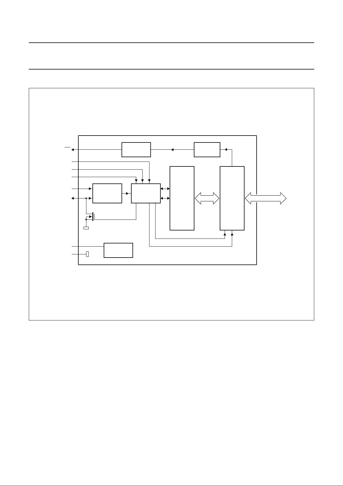
2 GENERAL DESCRIPTION
The PCF8575 is a silicon CMOS circuit. It provides general
purpose remote I/O expansion for most microcontroller
families via the two-line bidirectional bus (I
2
C-bus).
PCF8575
The device consists of a 16-bit quasi-bidirectional port and
2
an I
C-bus interface. The PCF8575 has a low current
consumption and includes latched outputs with high
current drive capability for directly driving LEDs. It also
possesses an interrupt line (INT) which can be connected
to the interrupt logic of the microcontroller. By sending an
interrupt signal on this line, the remote I/O can inform the
microcontroller if there is incoming data on its ports without
having to communicate via the I2C-bus. This means that
the PCF8575 is an I2C-bus slave transmitter/receiver.
Every data transmission from the PCF8575 must consist
of an even number of bytes, the first byte will be referred
to as P07 to P00 and the second byte as P17 to P10.
The third will be referred to as P07 to P00 and so on.
3 ORDERING INFORMATION
TYPE
NUMBER
PCF8575TS SSOP24 plastic shrink small outline package; 24 leads; body width 5.3 mm SOT340-1
NAME DESCRIPTION VERSION
PACKAGE
1999 Apr 07 3
Philips Semiconductors Product specification
Remote 16-bit I/O expander for I2C-bus
4 BLOCK DIAGRAM
handbook, full pagewidth
INT
A0
A1
A2
SCL
SDA
1
21
2
3
22
23
INPUT
FILTER
INTERRUPT
LOGIC
I2C-BUS
CONTROL
PCF8575
SHIFT
REGISTER
LP FILTER
16 BITS
I/O
PORT
PCF8575
P00 to P07
4 to 11
P10 to P17
13 to 20
WRITE pulse
DD
SS
24
12
POWER-ON
RESET
V
V
READ pulse
MGL537
Fig.1 Block diagram.
1999 Apr 07 4

Philips Semiconductors Product specification
Remote 16-bit I/O expander for I2C-bus
5 PINNING
SYMBOL PIN DESCRIPTION
INT 1 interrupt output (active LOW)
A1 2 address input 1
A2 3 address input 2
P00 4 quasi-bidirectional I/O 00
P01 5 quasi-bidirectional I/O 01
P02 6 quasi-bidirectional I/O 02
P03 7 quasi-bidirectional I/O 03
P04 8 quasi-bidirectional I/O 04
P05 9 quasi-bidirectional I/O 05
P06 10 quasi-bidirectional I/O 06
P07 11 quasi-bidirectional I/O 07
V
SS
P10 13 quasi-bidirectional I/O 10
P11 14 quasi-bidirectional I/O 11
P12 15 quasi-bidirectional I/O 12
P13 16 quasi-bidirectional I/O 13
P14 17 quasi-bidirectional I/O 14
P15 18 quasi-bidirectional I/O 15
P16 19 quasi-bidirectional I/O 16
P17 20 quasi-bidirectional I/O 17
A0 21 address input 0
SCL 22 serial clock line input
SDA 23 serial data line input/output
V
DD
12 supply ground
24 supply voltage
handbook, halfpage
INT
A1
A2
P00
P01
P02
1
2
3
4
5
6
24
23
22
21
20
19
PCF8575
P03
P04
P05
P06
P07
V
SS
7
8
9
10
11
12
18
17
16
15
14
13
MGL538
Fig.2 Pin configuration.
PCF8575
V
DD
SDA
SCL
A0
P17
P16
P15
P14
P13
P12
P11
P10
1999 Apr 07 5
Philips Semiconductors Product specification
Remote 16-bit I/O expander for I2C-bus
6 CHARACTERISTICS OF THE I2C-BUS
The I2C-bus is for bidirectional, 2-line communication
between different ICs or modules. The two lines are a
serial data line (SDA) and a serial clock line (SCL). Both
lines must be connected to a positive supply via a pull-up
resistor when connected to the output stages of a device.
Data transfer may be initiated only when the bus is not
busy.
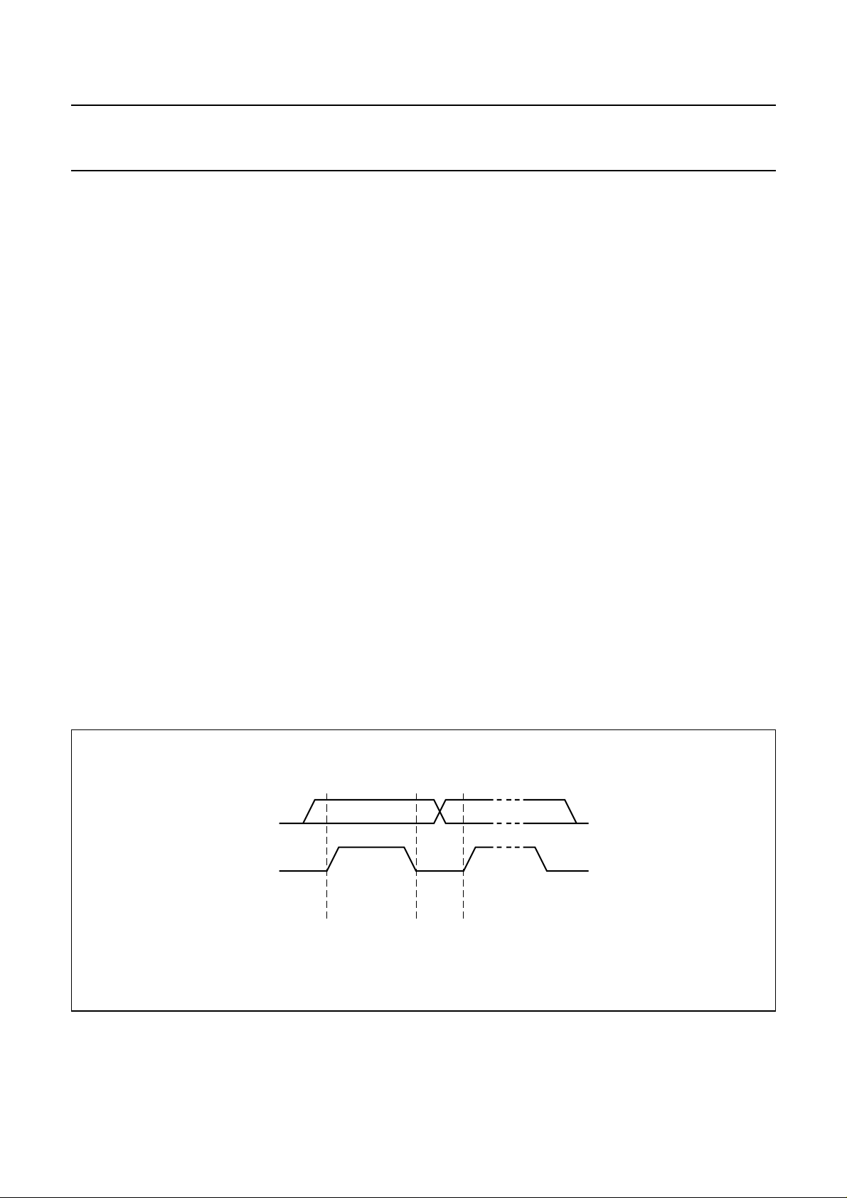
6.1 Bit transfer
One data bit is transferred during each clock pulse.
The data on the SDA line must remain stable during the
HIGH period of the clock pulse as changes in the data line
at this time will be interpreted as control signals
(see Fig.3).
6.2 START and STOP conditions
Both data and clock lines remain HIGH when the bus is not
busy. A HIGH-to-LOW transition of the data line, while the
clock is HIGH is defined as the START condition (S).
A LOW-to-HIGH transition of the data line while the clock
is HIGH is defined as the STOP condition P (see Fig.4).
PCF8575
6.4 Acknowledge
The number of data bytes transferred between the START
and the STOP conditions from transmitter to receiver is not
limited. Each byte of eight bits is followed by one
acknowledge bit. The transmitter must release the SDA
line before the receiver can send an acknowledge bit.
A slave receiver which is addressed must generate an
acknowledge after the reception of each byte. Also a
master must generate an acknowledge after the reception
of each byte that has been clocked out of the slave
transmitter. The device that acknowledges has to pull
down the SDA line during the acknowledge clock pulse, so
that the SDA line is stable LOW during the HIGH period of
the acknowledge related clock pulse, set-up and hold
times must be taken into account.
A master receiver must signal an end of data to the
transmitter by not generating an acknowledge after the
last byte that has been clocked out of the slave. This is
done by the master receiver by holding the SDA line HIGH.
In this event the transmitter must release the data line to
enable the master to generate a STOP condition.
6.3 System configuration
A device generating a message is a ‘transmitter’, a device
receiving the message is the ‘receiver’. The device that
controls the message is the ‘master’ and the devices which
are controlled by the master are the ‘slaves’ (see Fig.5).
handbook, full pagewidth
SDA
SCL
data line
stable;
data valid
Fig.3 Bit transfer.
change
of data
allowed
MBC621
1999 Apr 07 6

Philips Semiconductors Product specification
Remote 16-bit I/O expander for I2C-bus
handbook, full pagewidth
SDA
SCL
S
START condition
Fig.4 Definition of START and STOP conditions.
SDA
SCL
P
STOP condition
PCF8575
SDA
SCL
MBC622
handbook, full pagewidth
MASTER
TRANSMITTER /
RECEIVER
DATA OUTPUT
BY TRANSMITTER
DATA OUTPUT
BY RECEIVER
SCL FROM
MASTER
RECEIVER
S
START
condition
SLAVE
SLAVE
TRANSMITTER /
RECEIVER
Fig.5 System configuration.
MASTER
TRANSMITTER
not acknowledge
acknowledge
MASTER
TRANSMITTER /
RECEIVER
9821
clock pulse for
acknowledgement
MGL539
MBA605
Fig.6 Acknowledgment on the I2C-bus.
1999 Apr 07 7
Philips Semiconductors Product specification
Remote 16-bit I/O expander for I2C-bus
PCF8575
7 FUNCTIONAL DESCRIPTION
7.1 Quasi-bidirectional I/Os
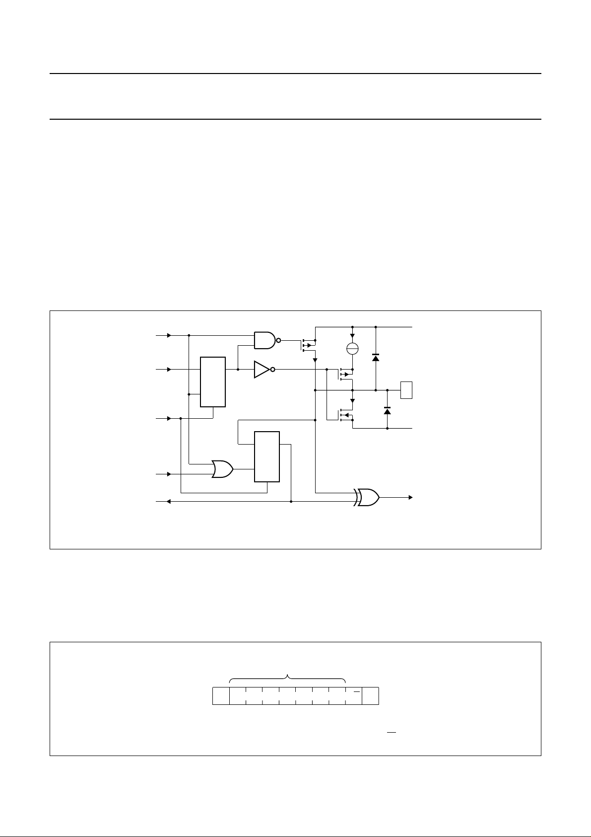
The PCF8575’s 16 ports (see Fig.7) are entirely independent and can be used either as input or output ports. Input data
is transferred from the ports to the microcontroller in the READ mode (see Fig.10). Output data is transmitted to the ports
in the WRITE mode (see Fig.9).
This quasi-bidirectional I/O can be used as an input or output without the use of a control signal for data direction.
At power-on the I/Os are HIGH. In this mode only a current source (I
VDD (I
) allows fast rising edges into heavily loaded outputs. These devices turn on when an output is written HIGH,
OHt
) to VDD is active. An additional strong pull-up to
OH
and are switched off by the negative edge of SCL. The I/Os should be HIGH before being used as inputs. After power-on
as all the I/Os are set HIGH all of them can be used as input. Any change in setting of the I/Os as either inputs or outputs
can be done with the write mode. Warning: If a HIGH is applied to an I/O which has been written earlier to LOW, a large
current (IOL) will flow to VSS. (see Characteristics note 3).
MGL540
V
DD
P00 to P07
P10 to 17
V
SS
to interrupt
logic
book, full pagewidth
write pulse
data from
shift register
power-on
reset
read pulse
data to
shift register
DQ
FF
C
I
S
D
FF
C
I
I
OH
100
I
OHt
Q
S
µA
I
OL
Fig.7 Simplified schematic diagram of each I/O.
7.2 Addressing
Figures 8, 9 and 10 show the address and timing diagrams. Before any data is transmitted or received the master must
send the address of the receiver via the SDA line. The first byte transmitted after the START condition carries the address
of the slave device and the read/write bit. The address of the slave device must not be changed between the START and
the STOP conditions. The PCF8575 acts as a slave receiver or a slave transmitter.
handbook, halfpage
S 0 1 0 0 A2 A1 A0 R/W A
slave address
MGL541
Fig.8 Byte containing the slave address and the R/W bits.
1999 Apr 07 8
 Loading...