

Philips PCF8558U-12-F2, PCF8558U-2-F2, PCF8558U-9-F2 Datasheet
DATA SH EET
Objective specification
Supersedes data of 1997 Feb 27
File under Integrated Circuits, IC12
1998 Apr 07
INTEGRATED CIRCUITS
PCF8558
Universal LCD driver for small
graphic panels
1998 Apr 07 2
Philips Semiconductors Objective specification
Universal LCD driver for small graphic
panels
PCF8558
FEATURES
• Single-chip LCD controller/driver
• 40 row and 101 column outputs
• Display data RAM
40 × 101 bits = 505 bytes = 4040 bits
• On-chip:
– Generation of intermediate LCD bias voltages
– Oscillator requires no external components
(external clock also possible)
• 400 kHz fast I2C-bus interface
• CMOS compatible
• MUX rate 1 : 40
• Logic supply voltage range V
DD
− VSS= 2.5 to 6 V
• Display supply voltage range VDD− V
LCD
= 3.5 to 9 V
• Low power consumption, suitable for battery operated
systems.
APPLICATIONS
• Telecom equipment
• Portable instruments
• Point of sale terminals
• Alarm systems.
GENERAL DESCRIPTION
The PCF8558 is a low power CMOS LCD controller driver,
designed to drive a graphic display of 40 rows and
101 columns. All necessary functions for the display are
provided in a single chip, including on-chip generation of
LCD bias voltages, resulting in a minimum of external
components and lower power consumption.
The PCF8558 interfaces to most microcontrollers via a
I
2
C-bus interface.
ORDERING INFORMATION
Note
1. For further details see Chapter “Bonding pad locations”.
TYPE
NUMBER
PACKAGE
(1)
NAME DESCRIPTION VERSION
PCF8558U/10 − chip on FFC −
PCF8558U/12 − chip with bumps on FFC −
1998 Apr 07 3
Philips Semiconductors Objective specification
Universal LCD driver for small graphic
panels
PCF8558
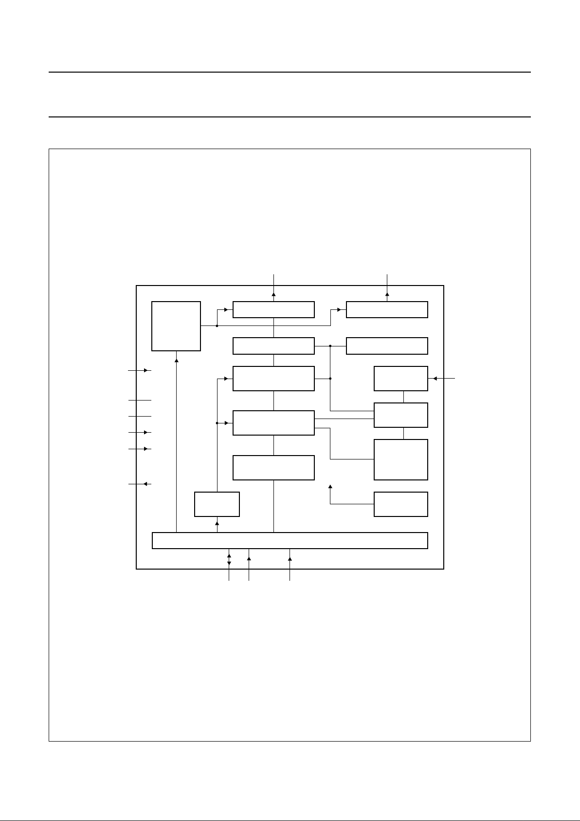
BLOCK DIAGRAM
Fig.1 Block diagram.
handbook, full pagewidth
MGG558
COLUMN DRIVERS
DATA LATCHES
CURSOR AND
DATA CONTROL
DISPLAY DATA RAM
505 BYTES
ADDRESS
COUNTER
DATA
REGISTER
ROW DRIVERS
SHIFT REGISTER
OSCILLATOR
TIMING
GENERATOR
DISPLAY
ADDRESS
COUNTER
POWER-ON
RESET
I/O BUFFER
BIAS
VOLT AGE
GENERATOR
V
LCD
V
DD
V
SS
T1
T3
T2
SDA SCL SA0
OSC
C1 to C101 R1 to R40
PCF8558
1998 Apr 07 4
Philips Semiconductors Objective specification
Universal LCD driver for small graphic
panels
PCF8558
PINNING
SYMBOL PAD DESCRIPTION
SCL 1 I
2
C-bus serial clock input
R20 to R1 2 to 21 LCD row driver data outputs
C101 to C1 22 to 122 LCD column driver data outputs
R21 to R40 123 to 142 LCD row driver data outputs
T2 143 test pad output, must be left unconnected (not user accessible)
SDA 144 I
2
C-bus serial data input/output
V
SS
145 ground
T1 146 test pad input, must be connected to V
SS
(not user accessible)
V
LCD
147 negative supply voltage input
SA0 148 the LSB bit of the I
2
C-bus slave address input is set by connecting this pin to either
0(VSS) or 1 (VDD)
T3 149 test pad input, must be connected to V
DD
(not user accessible)
OSC 150 when the on-chip oscillator is used this pin must be connected to V
DD
; an external clock
signal, if used, is input at this pin
V
DD
151 positive supply voltage

1998 Apr 07 5
Philips Semiconductors Objective specification
Universal LCD driver for small graphic
panels
PCF8558
FUNCTIONAL DESCRIPTION
LCD bias voltage generator
The intermediate bias voltages for the LCD display are
generated and buffered on-chip. This removes the need
for an external resistor bias chain and significantly reduces
the system power consumption.
Oscillator
The on-chip oscillator provides the clock signal for the
display system. No external components are required and
the OSC pin must be connected to V
DD
.
External clock
If an external clock is to be used it is input at the OSC pin.
The resulting display frame frequency is given by
.
Only in the power-down state is the clock allowed to be
stopped (OSC connected to V
SS
), otherwise the LCD will
be frozen in a state where a DC voltage is applied to it.
Power-on reset
The on-chip power-on reset block initializes the chip after
power-on or power failure. This is a synchronous reset and
requires 2 oscillator cycles to execute. These oscillator
cycles must be provided from the external clock source if
the internal oscillator is not used. If this is not done, the
device may not respond to command sequences
transmitted via the I
2
C-bus interface.
Power-down
The chip can be put into power-down mode where all static
currents are switched off (no internal oscillator, no internal
power-on reset, no bias level generation and all LCD
outputs are internally connected to V
DD
) when
PD = logic 1.
During power-down the information in the RAMs and the
internal chip states are preserved. Instruction execution
during power-down is possible if an externally clock signal
is applied to pad OSC.
Registers
The PCF8558 has one 8-bit register, time shared as a
Command Register (CR) and a Data Register (DR).
The command register stores the command code such as
display on or display off and address information for the
f
frame
f
OSC
3072
------------ -
=
Display Data RAM (DDRAM). Both registers can be written
to but not read from by the system controller.
Address Counter (AC)
The address counter assigns addresses to the DDRAM for
writing and is set by Y2 to Y0 in the command and
X6 to X0 in the address. After a write operation the
address counter is automatically incremented by 1 in
accordance with the V flag.
Display Data RAM (DDRAM)
The PCF8558 contains a 40 × 101-bit static RAM which
stores the display data. The RAM is divided into 5 banks of
101 bytes (5 × 8 × 101 bits). During RAM access, data is
transferred to the RAM via the I
2
C-bus. There is a direct
correspondence between the X address and the column
output number.
Timing generator
The timing generator produces the various signals
required to drive the internal circuitry. Internal chip
operation is not disturbed by operations on the data buses.
Display control
The display is generated by continuously shifting rows of
RAM data to the dot matrix LCD via the column outputs.
The display status (all dots on/off and normal/inverse
video) is set by bits E and D in the command word.
LCD row and column drivers
The PCF8558 contains 40 row and 101 column drivers,
which connect the appropriate LCD bias voltages in
sequence to the display in accordance with the data to be
displayed. Figure 3 illustrates typical waveforms. Unused
outputs should be left unconnected.
The bias voltage levels, V2 to V5, are chosen to give
optimum display contrast for a multiplex rate of 1 : 40.
Table 1 Voltage bias levels
LEVEL VOLTAGE
V2 0.8635 × (V
DD
− V
LCD
)
V3 0.7270 × (V
DD
− V
LCD
)
V4 0.2730 × (V
DD
− V
LCD
)
V5 0.1365 × (V
DD
− V
LCD
)
1998 Apr 07 6
Philips Semiconductors Objective specification
Universal LCD driver for small graphic
panels
PCF8558
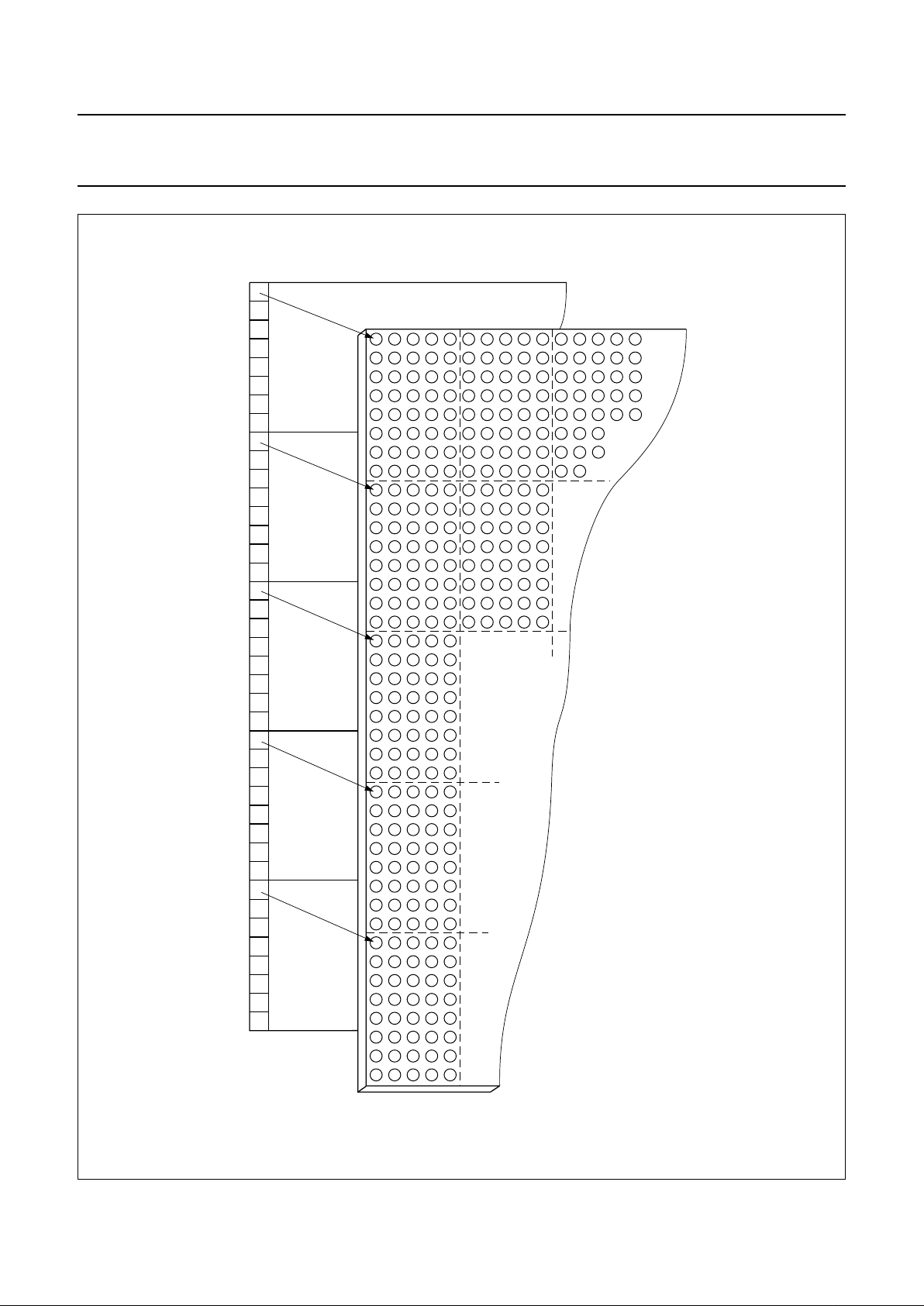
Fig.2 DDRAM to display mapping.
top of LCD
MGG559
RAM
bank 0
bank 1
bank 2
bank 3
bank 4
LCD
1998 Apr 07 7
Philips Semiconductors Objective specification
Universal LCD driver for small graphic
panels
PCF8558
Fig.3 Typical LCD driver waveforms (MUX rate 1 : 40).
V
state1
(t)
=C2
(t)
− R1
(t)
; V
state2
(t)
=C2
(t)
− R2
(t)
.
MGG560
ROW 1
R1 (t)
ROW 2
R2 (t)
COL 1
C1 (t)
COL 2
C2 (t)
0 V
V
DD
V
2
V
3
V
4
V
5
V
LCD
V
DD
V
2
V
3
V
4
V
5
V
LCD
V
DD
V
2
V
3
V
4
V
5
V
LCD
V
DD
V
2
V
3
V
4
V
5
V
LCD
0.2731V
OP
0.2731V
OP
0.7269V
OP
0.7269V
OP
V
OP
V
OP
0 V
0.2731V
OP
0.2731V
OP
0.7269V
OP
0.7269V
OP
V
OP
V
OP
frame n frame n + 1
123456789 123456789
... 40 ... 40
V
state 1
(t)
V
state 2
(t)
V
state 1
(t)
V
state 2
(t)
1998 Apr 07 8
Philips Semiconductors Objective specification
Universal LCD driver for small graphic
panels
PCF8558
ADDRESSING
The data is downloaded into the matrix of the PCF8558 as indicated in Figs 4 and 5.
The display RAM has a matrix of 40 by 101 bits (5 by 101 bytes). The columns are addressed by the address pointer.
After writing one byte the pointer is set to the next byte. Control of address increment, horizontal or vertical, is by bit V in
the command byte.
DATA STRUCTURE
Fig.4 RAM format, addressing.
handbook, full pagewidth
MGG561
display line 0 to 7
display line 8 to 15
display line 16 to 23
address 2
address 1
address 0
display line 24 to 31
display line 32 to 39
000
LSB
MSB
001
010 Y address
011
100
X
address 98
address 99
address 100
Fig.5 Order of writing data bytes into RAM.
handbook, full pagewidth
05
16
27
38
49
MGG562
0
101
202
303
404
1
102
203
304
405
2
103
204
305
406
. . .
. . .
. . .
. . .
. . .
a. Order of writing data bytes into RAM (V =1). b. Order of writing data bytes into RAM (V =0).
 Loading...