

Philips pcf8549, pcf8549 n DATASHEETS
INTEGRATED CIRCUITS
DATA SH EET
PCF8549
65 × 102 pixels matrix LCD driver
Product specification
File under Integrated Circuits, IC12
1997 Nov 21

Philips Semiconductors Product specification
65 × 102 pixels matrix LCD driver PCF8549
FEATURES
• Single chip LCD controller/driver
• 65 row and 102 column outputs
• Display data RAM 65 × 102 bits
• On-chip:
– Generation of LCD supply voltage
– Generation of intermediate LCD bias voltages
– Oscillator requires no external components (external
clock also possible)
• 400 kHz Fast I2C Interface
• CMOS compatible inputs
• Mux rate: 65
• Logic supply voltage range V
• Voltage generator voltage range V
− VSS: 1.5 to 6 V
DD1
DD2/2_HV
− VSS:
2.4 to 5 V
• Display supply voltage range V
− VSS: 7.0 to 16 V
LCD
• Low power consumption, suitable for battery operated
systems
• Temperature compensation of V
LCD
• Interlacing for better display quality
• Slim chip layout, suited for chip-on-glass applications.
GENERAL DESCRIPTION
The PCF8549 is a low power CMOS LCD controller driver,
designed to drive a graphic display of 65 rows and
102 columns. All necessary functions for the display are
provided in a single chip, including on-chip generation of
LCD supply and bias voltages, resulting in a minimum of
external components and low power consumption. The
PCF8549 interfaces to most microcontrollers via an
I2C interface.
Packages
The PCF8549U/2 is available as bumped die. Sawn wafer
as chip sorted in chip tray. For further details see
Section “Bonding pads”.
Customized TCP upon request.
APPLICATIONS
• Telecom equipment
• Portable instruments
• Point of sale terminals.
ORDERING INFORMATION
TYPE NUMBER
NAME DESCRIPTION VERSION
PCF8549U/2/F1 TRAY chip with bumps in tray
PACKAGE
1997 Nov 21 2
Philips Semiconductors Product specification
65 × 102 pixels matrix LCD driver PCF8549
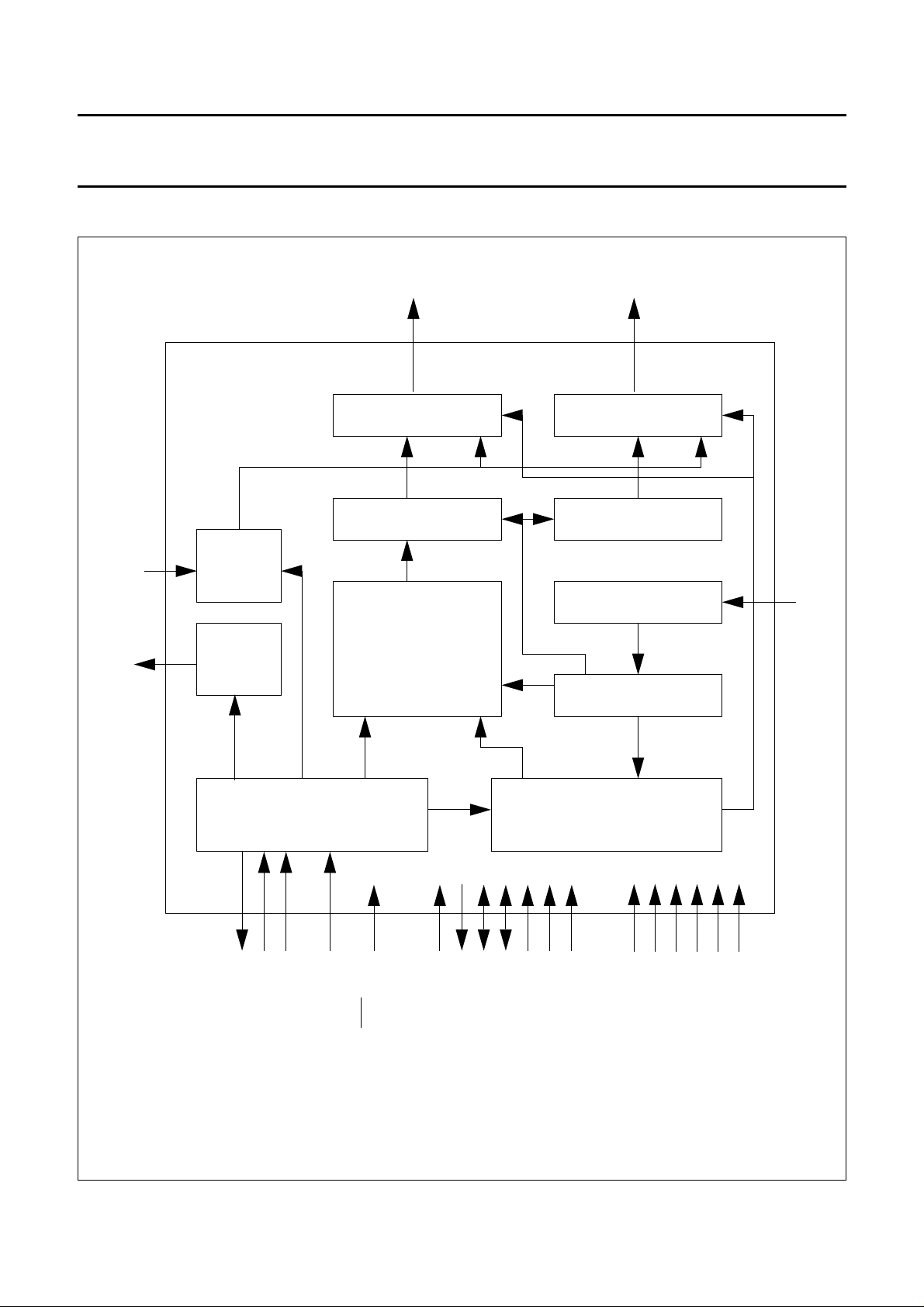
BLOCK DIAGRAM
VLCD2
VLCD1
Bias voltage generator
HVGEN
7 stages
C0 to C101
COLUMN DRIVERS
DATA LATCHES
Dual Ported RAM
65x102 Bit
R0 to R64
ROW DRIVERS
SHIFT REGISTER
OSCILLATOR
TIMING GENERATOR
OSC
IIC INTERFACE
SDA_out
SDA
SCL
1997 Nov 21 3
SA0
RES
Fig.1 Block diagram.
T1
DISPLAY CONTROL LOGIC
T3
T4
T2
T5T6T7
VDD1
VDD2
VDD2_HV
VSS1
VSS2
VSS2_HV
Philips Semiconductors Product specification
65 × 102 pixels matrix LCD driver PCF8549
PINNING
SYMBOL DESCRIPTION
R0 to R64 LCD row driver outputs
C0 to C101 LCD column driver outputs
V
SS1,2,2_HV
V
DD1,2,2_HV
V
LCD1,2
T1 test 1 input
T2 test 2 output
T3 test 3 I/O
T4 test 4 I/O
T5 test 5 input
T6 test 6 input
T7 test 7 input
SDA I
SCL I
SDA_OUT I
SA0 least significant bit of slave address
OSC oscillator
RES external reset input, low active
negative power supply
supply voltage
LCD supply voltage
2
C data input
2
C clock line
2
C output
Pin functions
R0 TO R64: ROW DRIVER OUTPUTS
These pads output the row signals.
TO C101: COLUMN DRIVER OUTPUTS
C0
These pads output the column signals.
V
SS1,2,2_HV
: NEGATIVE POWER SUPPLY RAILS
Negative power supplies.
V
DD1,2,2_HV
V
DD2
: POSITIVE POWER SUPPLY RAILS
and V
are the supply voltages for the internal voltage generator. Both have to be on the same voltage and
DD2_HV
may be connected together outside of the chip. If the internal voltage generator is not used, they should be both
connected to ground. V
V
DD2
V
LCD1,2
and V
: LCD POWER SUPPLY
DD2_HV
.
is used as power supply for the rest of the chip. This voltage can be a different voltage than
DD1
Positive power supply for the liquid crystal display. If the internal voltage generator is used, the two supply rails
V
LCD1
case, V
and V
LCD1
must be connected together. An external LCD supply voltage can be supplied using the V pad. In this
LCD2
has to be connected to ground, and the internal voltage generator has to be programmed to zero. If the
PCF8549 is in power-down mode, the external LCD supply voltage has to be switched off.
1997 Nov 21 4

Philips Semiconductors Product specification
65 × 102 pixels matrix LCD driver PCF8549
T1, T2, T3, T4, T5, T6 AND T7: TEST PADS
T1, T3, T4, T5, T6 and T7 must be connected to V
SS1
, T2
is to be left open. Not accessible to user.
2
SDA/SDA_OUT: I
CDATA LINES
Output and input are separated. If both pads are
connected together they behave like a standard I2C pad.
2
SCL: I
C CLOCK SIGNAL
Input for the I2C-bus clock signal.
LAVE ADDRESS
SA0: S
With the SA0 pin two different slave addresses can be
selected. That allows to connect two PCF8549 LCD
drivers to the same I2C-bus.
OSCILLATOR
OSC:
When the on-chip oscillator is used this input must be
connected to V
. An external clock signal, if used, is
DD1
connected to this input.
RES: RESET
FUNCTIONAL DESCRIPTION
Block diagram functions
O
SCILLATOR
The on-chip oscillator provides the clock signal for the
display system. No external components are required and
the OSC input must be connected to V
. An external
DD1
clock signal, if used, is connected to this input.
2
CINTERFACE
I
The I2C interface receives and executes the commands
sent via the I2C-bus. It also receives RAM-data and sends
them to the RAM. During read access the 8-bit parallel
data or the status register content is converted to a serial
data stream and output via the I2C-bus.
D
ISPLAY CONTROL LOGIC
The display control logic generates the control signals to
read out the RAM via the 101 bit parallel port. It also
generates the control signals for the row, and
column drivers.
ISPLAY DATA RAM (DDRAM)
D
This signal will reset the device. Signal is active low.
The PCF8549 contains a 65 × 102 bit static RAM which
stores the display data. The RAM is divided into 8 banks of
102 bytes and one bank of 102 bits
((8 × 8+1)×102 bits). During RAM access, data is
transferred to the RAM via the I2C interface. There is a
direct correspondence between X-address and column
output number.
IMING GENERATOR
T
The timing generator produces the various signals
required to drive the internal circuitry. Internal chip
operation is not disturbed by operations on the I2C-bus.
LCD
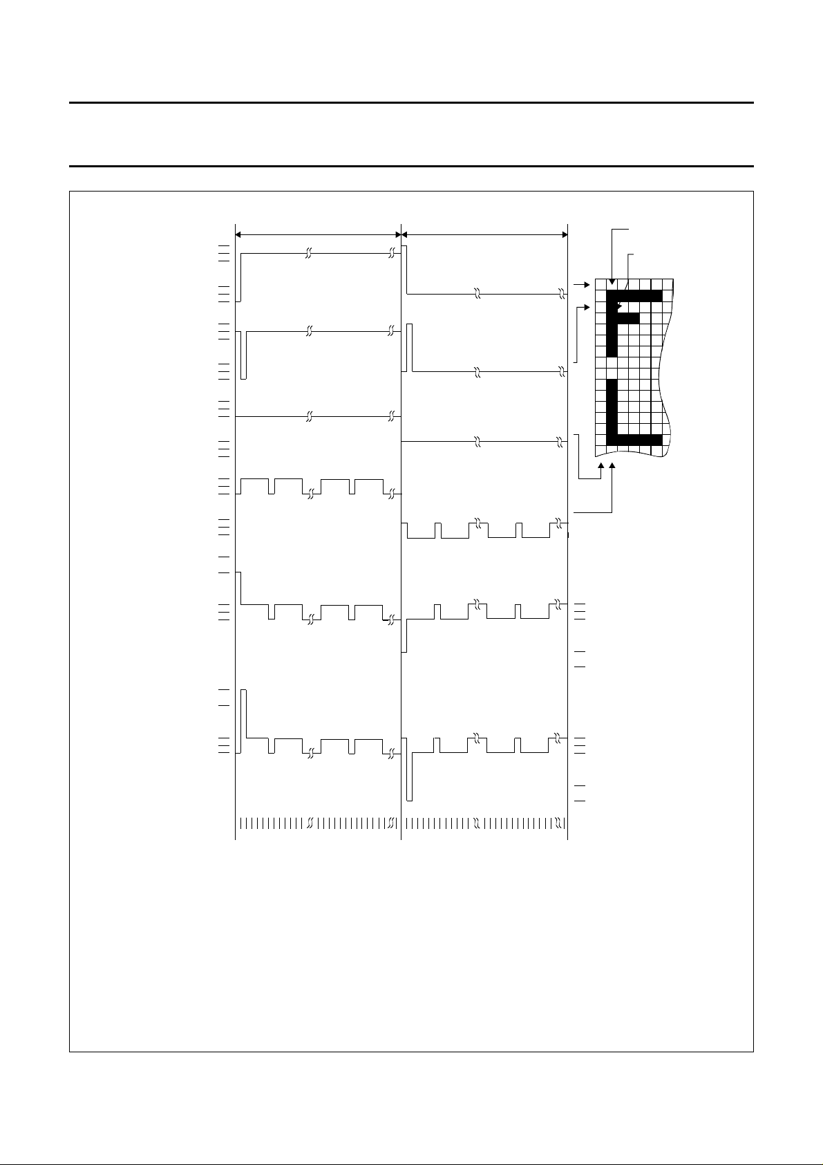
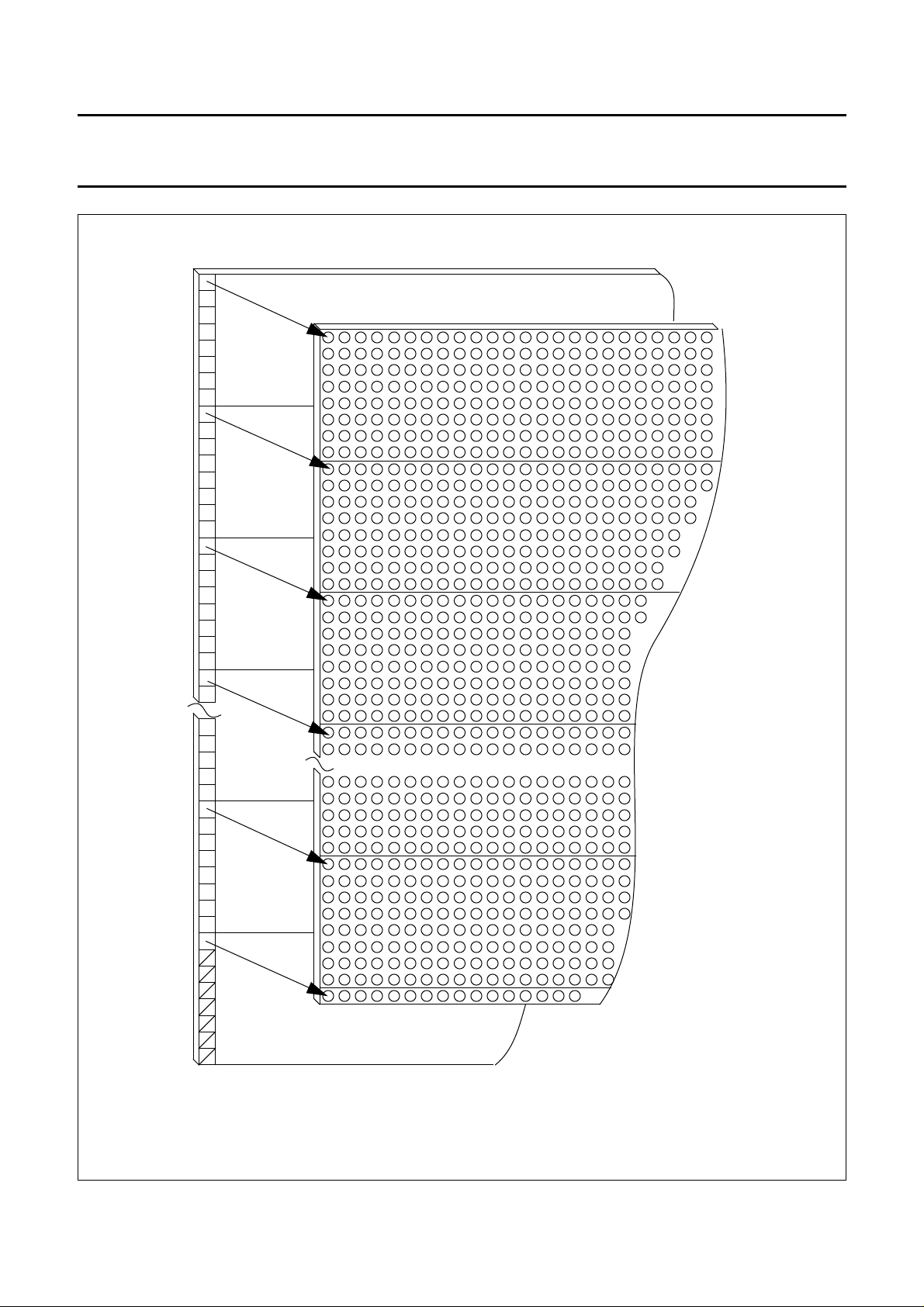
ROW AND COLUMN DRIVERS
The PCF8549 contains 65 row and 102 column drivers,
which connect the appropriate LCD bias voltages to the
display in accordance with the data to be displayed.
Figure 2 shows typical waveforms. Unused outputs should
be left unconnected.
1997 Nov 21 5
Philips Semiconductors Product specification
65 × 102 pixels matrix LCD driver PCF8549
ROW 0
R0 (t)
ROW 2
R2 (t)
COL 0
C0 (t)
COL 1
C1 (t)
V
LCD
V
3
(t)
V
LCD
0 V
state1
V3 - V
V
V
LCD
V
3
- V
frame n+1frame n
V
LCD
V
2
V
3
V
4
V
5
V
SS
V
LCD
V
2
V
3
V
4
V
5
V
SS
V
LCD
V
2
V
3
V
4
V
5
V
SS
V
LCD
V
2
V
3
V
4
V
5
V
SS
2
2
V4 - V
0 V
V
5
V4 - V
- V
LCD
5
LCD
V
V
state1
state2
(t)
(t)
(t)
V
- V
LCD
2
0 V
state2
V3 - V
2
V
0 2 4 6 8 10 ...
0 2 4 6 8 10 ...
V
(t) = C1(t) - R0(t)
state1
V
(t) = C1(t) - R2(t)
state2
... 64
1 3 5 7 9 ...
... 63
Fig.2 Typical LCD driver waveforms.
1997 Nov 21 6
... 64
1 3 5 7 9 ...
... 63
V4 - V
0 V
V
5
V4 - V
- V
LCD
VSS=0V
5
LCD
Philips Semiconductors Product specification
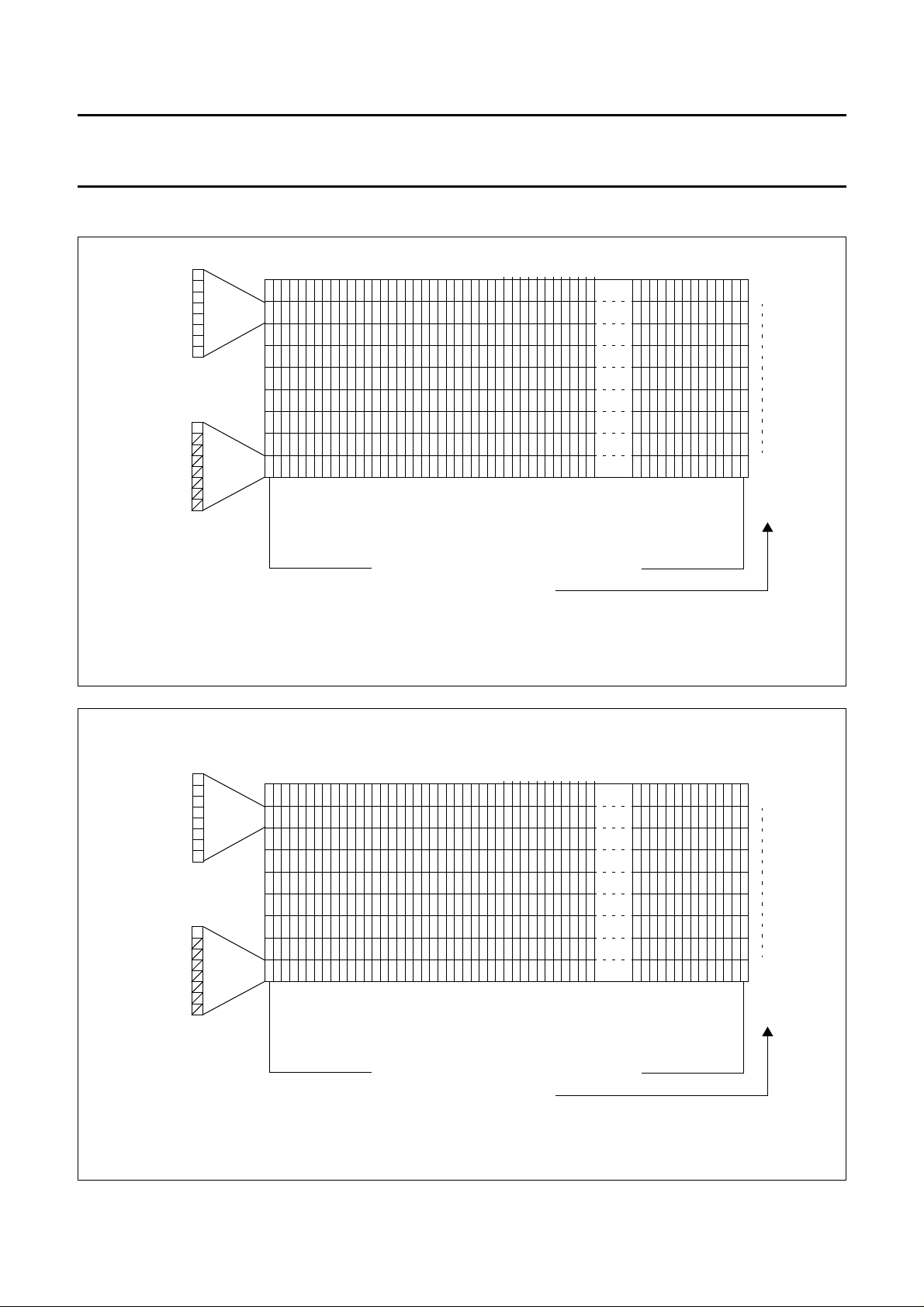
65 × 102 pixels matrix LCD driver PCF8549
DDRAM
bank 0
bank 1
bank 2
bank 3
bank 7
bank 8
Fig.3 DDRAM to display mapping.
1997 Nov 21 7

Philips Semiconductors Product specification
65 × 102 pixels matrix LCD driver PCF8549
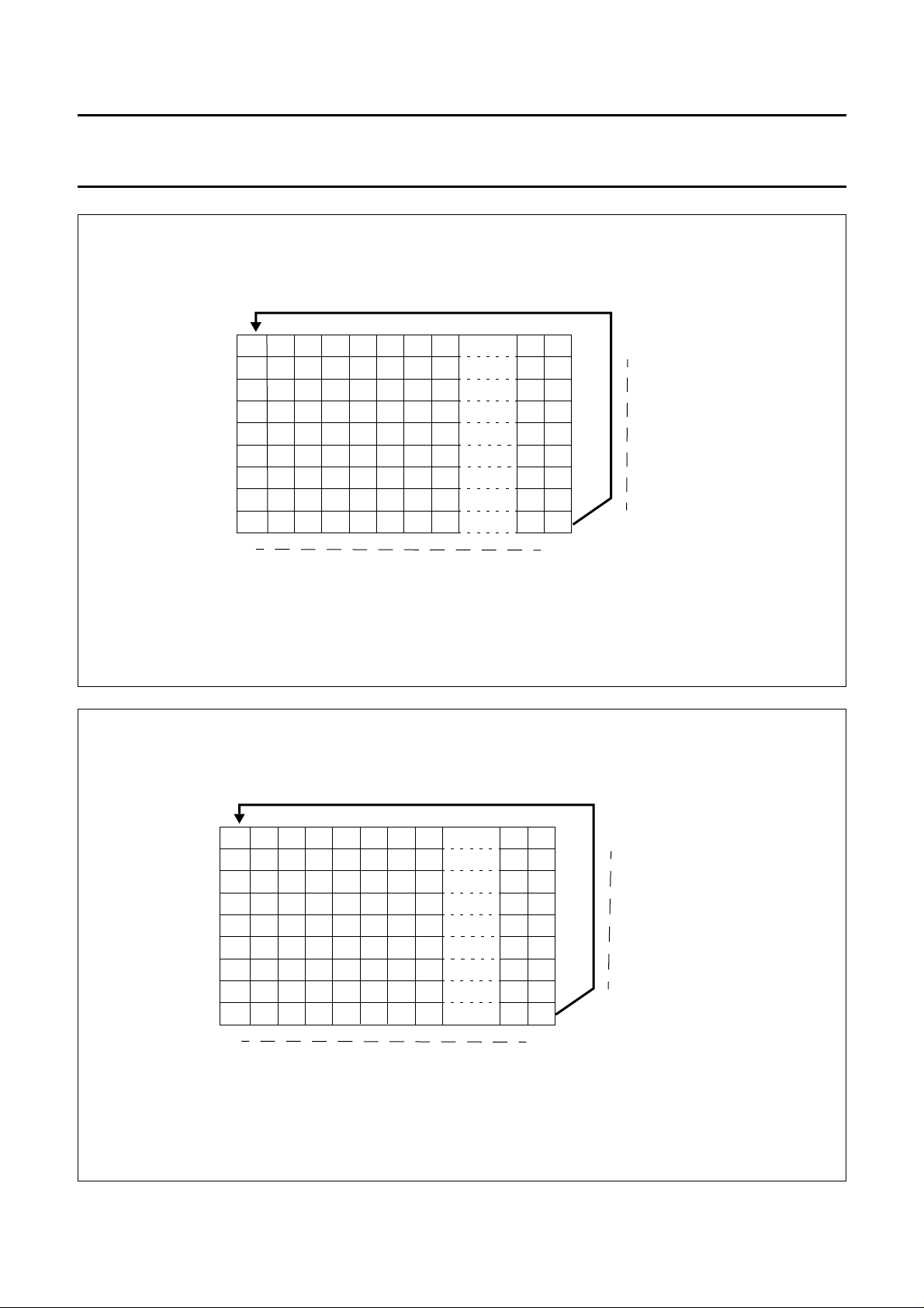
Addressing
The Display data RAM of the PCF8549 is accessed as
indicated in Figs 3, 4, 4, 6 and 7. The display RAM has a
matrix of 65 × 102 bits. The columns are addressed by the
address pointer. The address ranges are:
X 0 to 101 (1100101b) and Y 0 to 8 (1000b). Addresses
outside these ranges are not allowed. In vertical
addressing mode (V = 1) the Y address increments (see
Fig.7) after each byte. After the last Y address (Y = 8)
Y wraps around to 0 and X increments to address the next
column. In horizontal addressing mode (V = 0) the
X address increments (see Fig.6) after each byte. After the
last X address (X = 101) X wraps around to
0 and Y increments to address the next row. After the very
last address (X = 101 and Y = 8) the address pointers
wrap around to address (X = 0 and Y = 0).
The MX bit allows a horizontal mirroring: When MX = 1,
the X address space is mirrored: The addressX=0 is
then located at the right side (column 101) of the display
(see Fig.4). When MX = 0 the mirroring is disabled and the
address X = 0 is located at the left side (column 0) of the
display (see Fig.4).
If the RM-bit (read-modify-write mode) is set, the address
is only incremented after a write, otherwise the address is
incremented after both read and write access to the
display data RAM.
1997 Nov 21 8
Philips Semiconductors Product specification
65 × 102 pixels matrix LCD driver PCF8549
DISPLAY DATA RAM STRUCTURE
MSB
0
LSB
MSB
8
LSB
MSB
LSB
MSB
LSB
0 X-address
Y-address
Fig.4 RAM format, addressing (MX = 0).
101
0
8
101
Fig.5 RAM format, addressing (MX = 1).
1997 Nov 21 9
X-address
Y-address
0
Philips Semiconductors Product specification
65 × 102 pixels matrix LCD driver PCF8549
012
102 103 104
204 205 206
306 307 308
408 409 410
510 511 512
612 613 614
714 715 716
816 817 818 917
0
101
0
Y-address
8
X-address
Fig.6 Sequence of writing data bytes into RAM with horizontal addressing (V = 0).
09
1 10
2
3
4
5
6
7
8 917
0
Fig.7 Sequence of writing data bytes into RAM with vertical addressing (V = 1).
1997 Nov 21 10
0
Y-address
8
101
Philips Semiconductors Product specification
65 × 102 pixels matrix LCD driver PCF8549
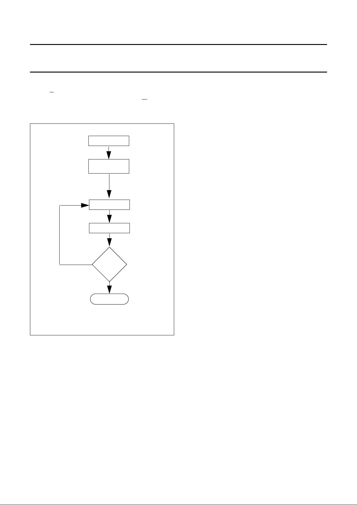
RAM access
If the D/C bit is 1 the RAM can be accessed in both read
and write access mode, depending on the R/W bit. The
data is written to the RAM during the acknowledge cycle.
Set Address
Set Read
Modify Write Mode
Read Data
Write Data
no
Finished?
period of the clock pulse as changes in the data line at this
time will be interpreted as a control signal.
TART AND STOP CONDITIONS (see Fig.10)
S
Both data and clock lines remain HIGH when the bus is not
busy. A HIGH-to-LOW transition of the data line, while the
clock is HIGH is defined as the START condition (S). A
LOW-to-HIGH transition of the data line while the clock is
HIGH is defined as the STOP condition (P).
YSTEM CONFIGURATION (see Fig.11)
S
• Transmitter: The device which sends the data to the bus
• Receiver: The device which receives the data from the
bus
• Master: The device which initiates a transfer, generates
clock signals and terminates a transfer
• Slave: The device addressed by a master
• Multi-Master: More than one master can attempt to
control the bus at the same time without corrupting the
message
• Arbitration: Procedure to ensure that, if more than one
master simultaneously tries to control the bus, only one
is allowed to do so and the message is not corrupted
• Synchronisation: Procedure to synchronize the clock
signals of two or more devices.
yes
END
Fig.8 Read modify write access.
2
C-BUS INTERFACE
I
2
Characteristics of the I
C-bus
The I2C-bus is for bi-directional, two-line communication
between different ICs or modules. The two lines are a
serial data line (SDA) and a serial clock line (SCL). Both
lines must be connected to a positive supply via a pull-up
resistor. Data transfer may be initiated only when the bus
is not busy.
IT TRANSFER (see Fig.9)
B
One data bit is transferred during each clock pulse. The
data on the SDA line must remain stable during the HIGH
CKNOWLEDGE (see Fig.12)
A
Each byte of eight bits is followed by an acknowledge bit.
The acknowledge bit is a HIGH signal put on the bus by
the transmitter during which time the master generates an
extra acknowledge related clock pulse. A slave receiver
which is addressed must generate an acknowledge after
the reception of each byte. Also a master receiver must
generate an acknowledge after the reception of each byte
that has been clocked out of the slave transmitter. The
device that acknowledges must pull-down the SDA line
during the acknowledge clock pulse, so that the SDA line
is stable LOW during the HIGH period of the acknowledge
related clock pulse (set-up and hold times must be taken
into consideration). A master receiver must signal an end
of data to the transmitter by not generating an
acknowledge on the last byte that has been clocked out of
the slave. In this event the transmitter must leave the data
line HIGH to enable the master to generate a stop
condition.
1997 Nov 21 11
 Loading...