

Philips PCF8548U-2, PCF8548U-9 Datasheet

INTEGRATED CIRCUITS
DATA SH EET
PCF8548
65 × 102 pixels matrix LCD driver
Product specification
Supersedes data of 1999 Mar 22
File under Integrated Circuits, IC12
1999 Aug 16

Philips Semiconductors Product specification
65 × 102 pixels matrix LCD driver PCF8548
CONTENTS
1 FEATURES
2 APPLICATIONS
3 GENERAL DESCRIPTION
3.1 Packages
4 ORDERING INFORMATION
5 BLOCK DIAGRAM
6 PINNING
7 PIN FUNCTIONS
7.1 R0 to R64: row driver outputs
7.2 C0 to C101: column driver outputs
7.3 V
7.4 V
7.5 V
7.6 V
7.7 V
and V
SS1
to V
DD1
LCDIN
LCDOUT
LCDSENSE
(V
DD3
: LCD power supply
: LCD power supply
: voltage multiplier regulation input
)
LCD
: negative power supply rails
SS2
: positive power supply rails
7.8 T1 to T12: test pads
7.9 SDAIN and SDAOUT: I2C-bus data lines
7.10 SCL: I2C-bus clock signal
7.11 SA0: slave address
7.12 OSC: oscillator
7.13 RES: reset
8 BLOCK DIAGRAM FUNCTIONS
8.1 Oscillator
8.2 I2C-bus interface
8.3 Display control logic
8.4 Display Data RAM (DDRAM)
8.5 Timing generator
8.6 LCD row and column drivers
9 INITIALIZATION
10 ADDRESSING
10.1 Display data RAM structure
10.2 RAM access
11 I2C-BUS INTERFACE
11.1 Characteristics of the I2C-bus
11.1.1 Bit transfer
11.1.2 START and STOP conditions
11.1.3 System configuration
11.1.4 Acknowledge
11.2 I2C-bus protocol
12 INSTRUCTIONS
12.1 External reset (RES)
12.2 Function set
12.2.1 Power-Down (PD)
12.2.2 V
12.2.3 H
12.2.4 MX
12.2.5 MY
12.3 Display control
12.3.1 D and E
12.4 Display configuration
12.4.1 TRS
12.4.2 BRS
12.5 Set Y address of RAM
12.6 Set X address of RAM
12.7 Set HV generator stages
12.7.1 S[1:0]
12.8 Temperature control
12.9 Bias system
12.10 Set VOP value
13 LIMITING VALUES
14 HANDLING
15 DC CHARACTERISTICS
16 AC CHARACTERISTICS
17 RESET
18 APPLICATION INFORMATION
19 CHIP INFORMATION
20 PAD INFORMATION
21 DEVICE PROTECTION DIAGRAM
22 TRAY INFORMATION
23 DEFINITIONS
24 LIFE SUPPORT APPLICATIONS
25 PURCHASE OF PHILIPS I2C COMPONENTS
26 BARE DIE DISCLAIMER
1999 Aug 16 2

Philips Semiconductors Product specification
65 × 102 pixels matrix LCD driver PCF8548
1 FEATURES
• Single-chip LCD controller/driver
• 65 row and 102 column outputs
• Display data RAM 65 × 102 bits
• On-chip:
– Configurable 5 (4, 3 and 2) × voltage multiplier
generating V
(external V
LCD
also possible)
LCD
– Generation of intermediate LCD bias voltages
– Oscillator requires no external components
(external clock also possible).
• 400 kbits/s fast I2C-bus interface
• CMOS compatible inputs
• Mux rate: 1 : 65
• Logic supply voltage range V
DD1
to VSS:
– 1.9 to 5.5 V.
• High voltage generator supply voltage range V
VSS and V
DD3
to VSS:
DD2
to
– 2.4 to 4.5 V with LCD voltage internally generated
(voltage generator enabled).
• Display supply voltage range V
LCD
to VSS:
– 4.5 to 9.0 V
• Low power consumption, suitable for battery operated
systems
• Temperature compensation of V
LCD
• Slim chip layout, suitable for Chip-On-Glass (COG)
applications
• Programmable bottom row pads mirroring and top row
pads mirroring, for compatibility with both Tape Carrier
Package (TCP) and COG applications.
2 APPLICATIONS
• Telecom equipment
• Portable instruments
• Point of sale terminals.
3 GENERAL DESCRIPTION
The PCF8548is a low power CMOS LCD controller driver,
designed to drive a graphic display of 65 rows and
102 columns. All necessary functions for the display are
provided in a single chip, including on-chip generation of
LCD supply and bias voltages, resulting in a minimum of
external components and low power consumption.
The PCF8548 interfaces to most microcontrollers via an
I2C-bus interface.
3.1 Packages
The PCF8548is available aschip with bumpsin tray;tape
carrier package is available on request.
4 ORDERING INFORMATION
PACKAGE
TYPE NUMBER
NAME DESCRIPTION VERSION
PCF8548U/2 Tray chip with bumps in tray −
PCF8548U/9 Bumped wafer quarter wafer −
1999 Aug 16 3
Philips Semiconductors Product specification
65 × 102 pixels matrix LCD driver PCF8548
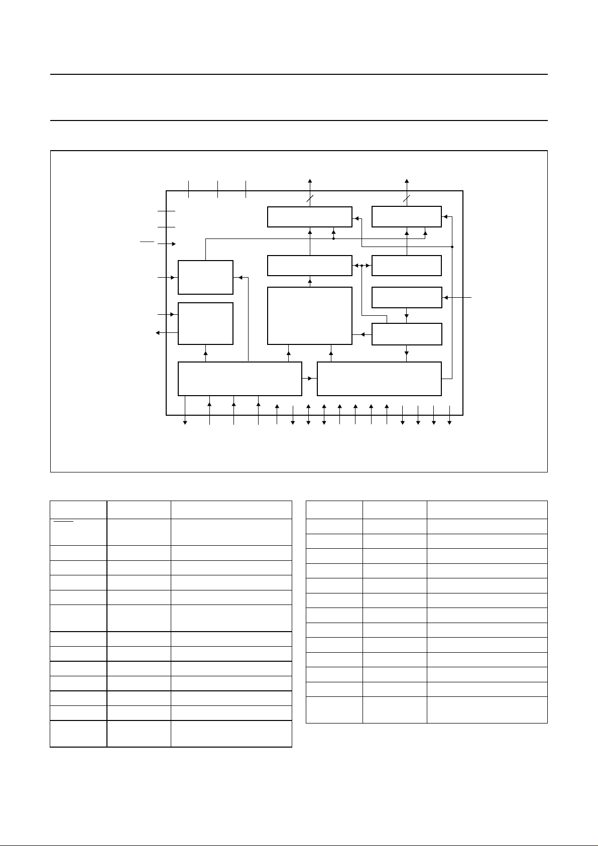
5 BLOCK DIAGRAM
V
handbook, full pagewidth
DD1
V
DD2VDD3
C0 to C101
R0 to R64
V
V
V
LCDIN
V
LCDSENSE
V
LCDOUT
SS1
SS2
RES
PCF8548
BIAS
VOLTAGE
GENERATOR
HIGH
VOLTAGE
GENERATOR
4 STAGES
INTERFACE
COLUMN DRIVERS
DISPLAY DATA RAM
2
C-BUS
I
SA0SDAOUT SDAIN SCL
T1 T2 T3 T4 T5 T6 T7 T8 T9 T10 T11 T12
Fig.1 Block diagram.
102
DATA LATCHES
65 × 102 BITS
65
ROW DRIVERS
SHIFT REGISTER
OSCILLATOR
TIMING
GENERATOR
DISPLAY CONTROL LOGIC
OSC
MGS393
6 PINNING
SYMBOL PAD DESCRIPTION
RES 1 external reset input (active
LOW)
2
SDAOUT 2 I
SDAIN 3 and 4 I
SCL 5 and 6 I
C-bus data output
2
C-bus data input
2
C-bus clock input
T2 7 test 2 output
SA0 8 least significant bit of slave
address
T7 to T5 9 to 11 test inputs
T4 and T3 12 and 13 test input/output
T1 14 test input
V
SS1
V
SS2
V
LCDOUT
V
LCDSENSE
15 to 20 negative power supply 1
21 to 26 negative power supply 2
28 to 33 voltage multiplier output
34 voltage multiplier
regulation input (V
LCD
)
SYMBOL PAD DESCRIPTION
V
LCDIN
35 to 40 LCD supply voltage
R32 to R19 41 to 54 LCD row driver outputs
R0 to R18 57 to 75 LCD row driver outputs
C0 to C101 76 to 177 LCD column driver outputs
R50 to R33 178 to 195 LCD row driver outputs
R51 to R64 198 to 211 LCD row driver outputs
T12 to T9 212 to 215 test outputs
OSC 216 oscillator
T8 217 test input
V
DD1
V
DD3
V
DD2
218 to 223 supply voltage 1
224 to 226 supply voltage 3
227 to 233 supply voltage 2
27, 55, 56,
dummy pads
196 and 197
1999 Aug 16 4

Philips Semiconductors Product specification
65 × 102 pixels matrix LCD driver PCF8548
7 PIN FUNCTIONS
7.1 R0 to R64: row driver outputs
These pads output the row signals.
7.2 C0 to C101: column driver outputs
These pads output the column signals.
7.3 V
V
is related to V
SS2
V
.
DD1
7.4 V
V
DD2
SS1
DD1
and V
and V
to V
DD3
: negative power supply rails
SS2
and V
DD2
: positive power supply rails
DD3
DD3
and V
is related to
SS1
are the supply voltages for the internal
voltage generator. Both have to be at the same voltage
and must beconnected together outside of the chip. If the
internal voltagegenerator isnot used, they should bothbe
connected to power or to the V
V
is used as the power supply for the rest of the chip.
DD1
This voltage can be a different voltage than V
V
.
DD3
7.5 V
: LCD power supply
LCDIN
DD1
pad.
DD2
and
Internally generated positive power supply for the liquid
crystal display. An external LCD supply voltage can be
supplied using the V
pad. In this case, V
LCDIN
LCDOUT
has
to be connected to ground, and the internal voltage
generator has to be programmed to zero. If the PCF8548
is in power-down mode, the external LCD supply voltage
must be switched off.
7.8 T1 to T12: test pads
T1 and T3 to T7 must be connected to V
connected to V
. T2 and T9 to T12 must be left
DD1
. T8 must be
SS1
open-circuit; not accessible to user.
2
7.9 SDAIN and SDAOUT: I
C-bus data lines
Serial data and acknowledge lines for the I2C-bus.
By connecting SDAINto SDAOUT,the SDA linebecomes
fully I2C-bus compatible. Having the acknowledge output
(SDAOUT) separated from the serial data line is
advantageous in Chip-On-Glass (COG) applications.
In COG applications where the track resistance from the
SDAOUT padto the system SDA line can besignificant, a
potential divider is generated by the bus pull-up resistor
and the Indium Tin Oxide (ITO) track resistance. It is
possible that during the acknowledge cycle the PCF8548
will not be able to create a valid logic 0 level. By splitting
the SDA input from the output thedevice could be used in
a mode that ignores the acknowledge bit. In COG
applications wherethe acknowledge cycleis required, it is
necessary to minimize the track resistance from the
SDACK pad to the system SDA line to guarantee a valid
LOW level.
7.10 SCL: I
2
C-bus clock signal
I2C-bus serial clock signal input.
7.11 SA0: slave address
Two different slave addresses can be selected using the
SA0 pad. This allows two PCF8548 LCD drivers to be
connected to the same I2C-bus.
7.6 V
: LCD power supply
LCDOUT
Positive power supply for the liquid crystal display. If the
internal voltage generator is used, the two supply rails
V
LCDIN
and V
must be connected together and an
LCDOUT
external capacitor must be connected (see Fig.19).
7.7 V
V
LCDSENSE
LCDSENSE
(V
LCD
is the input voltage for the internal voltage
: voltage multiplier regulation input
)
multiplier regulation.
If the internal voltage generator is used then V
must be connected to V
voltage is used then V
LCDSENSE
. If an external supply
LCDOUT
must be connected to
LCDSENSE
ground.
1999 Aug 16 5
7.12 OSC: oscillator
When the on-chip oscillator is used this input must be
connected to V
. An external clock signal, if used, is
DD1
connected to this input.
7.13 RES: reset
This signalis used toreset the device.The signal isactive
LOW.

Philips Semiconductors Product specification
65 × 102 pixels matrix LCD driver PCF8548
8 BLOCK DIAGRAM FUNCTIONS
8.1 Oscillator
The on-chip oscillator provides the clock signal for the
display system.No external componentsare required and
the OSC input must be connected to V
. An external
DD1
clock signal (if used), is connected to this input.
2
8.2 I
C-bus interface
The I2C-bus interface receives and executes the
commands sent viathe I2C-bus. It alsoreceives RAMdata
and sends it to the RAM.
8.3 Display control logic
The display control logic generates the control signals to
read from the RAM via the 102 bits parallel port. It also
generates the control signals for the row and column
drivers.
8.4 Display Data RAM (DDRAM)
The PCF8548 contains a 65 × 102 bit static RAM which
storesthe displaydata. TheRAM is dividedinto 8 banksof
102 bytes and 1 bank of 102 bits [(8 × 8+1)×102 bits].
DuringRAM access,data istransferred tothe RAMvia the
I2C-bus interface. There is a direct correspondence
between the X address and column output number.
8.5 Timing generator
The timing generator produces the various signals
required to drive the internal circuitry. Internal chip
operation is not disturbed by operations on the I
2
C-bus.
8.6 LCD row and column drivers
The PCF8548 contains 65 row and 102 column drivers,
which connect the appropriate LCD bias voltages to the
display in accordance with the data to be displayed.
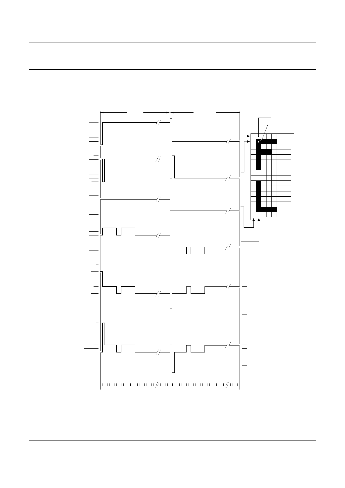
Figure 2shows typicalwaveforms.Unused outputsshould
be left unconnected.
9 INITIALIZATION
Immediately following Power-on, all internal registers and
theRAM contentare undefined.A resetpulse mustfirst be
applied.
Reset isaccomplished by applying an external RES pulse
(active LOW).When reset occurswithin the specified time
allinternal registersareinitialized, howeverthe RAM isstill
undefined. The state after reset is described in
Section 12.1.
The RES input must be ≤0.3 VDD when VDD reaches
V
(or higher)within a maximumtime t
DD(min)
VHRL
after V
DD
goes HIGH (see Fig.17).
1999 Aug 16 6
Philips Semiconductors Product specification
65 × 102 pixels matrix LCD driver PCF8548
ROW 0
R0 (t)
ROW 1
R1 (t)
COL 0
C0 (t)
COL 1
C1 (t)
V
LCD
V3 − V
V
V
V
V
V
V
V
V
V
V
V
V
V
V
V
V
V
V
V
V
V
V
V
V
LCD
2
3
4
5
SS
LCD
2
3
4
5
SS
LCD
2
3
4
5
SS
LCD
2
3
4
5
SS
− V
SS
SS
frame n frame n + 1
V
state1
V
state2
(t)
(t)
V
− V
LCD
V
V
V
(t) = C1(t) − R0(t).
state1
V
(t) = C1(t) − R1(t).
state2
state1
state2
(t)
(t)
0 V
V3 − V
V
LCD
V3 − V
V
LCD
0 V
V3 − V
2
SS
− V
SS
SS
− V
2
SS
012345678... ... 64 012345678... ... 64
Fig.2 Typical LCD driver waveforms.
1999 Aug 16 7
V4 − V
0 V
VSS − V
V4 − V
V
− V
SS
V4 − V
0 V
VSS − V
V4 − V
V
− V
SS
MGS671
5
5
LCD
LCD
5
5
LCD
LCD
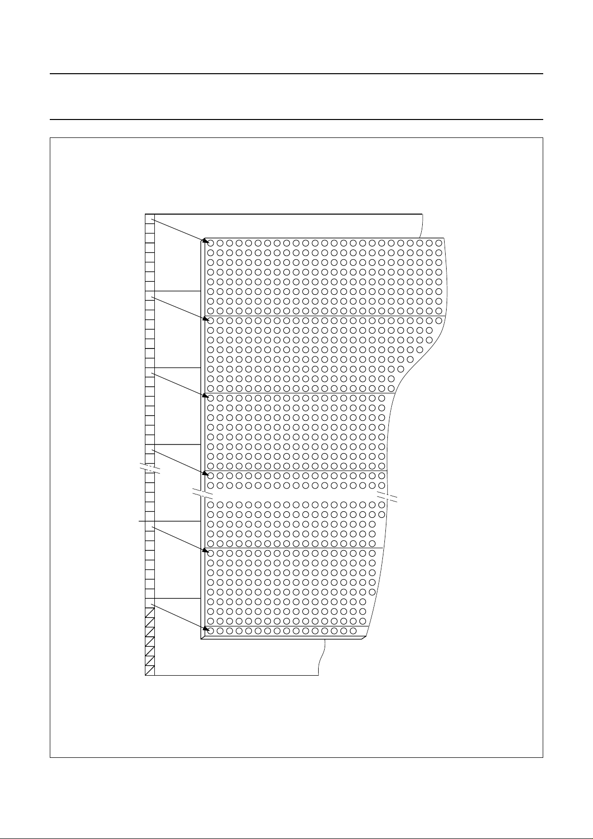
Philips Semiconductors Product specification
65 × 102 pixels matrix LCD driver PCF8548
DDRAM
bank 0
top of LCD
bank 1
bank 2
bank 3
bank 7
bank 8
LCD
Fig.3 DDRAM to display mapping.
1999 Aug 16 8
MGS395
Philips Semiconductors Product specification
65 × 102 pixels matrix LCD driver PCF8548
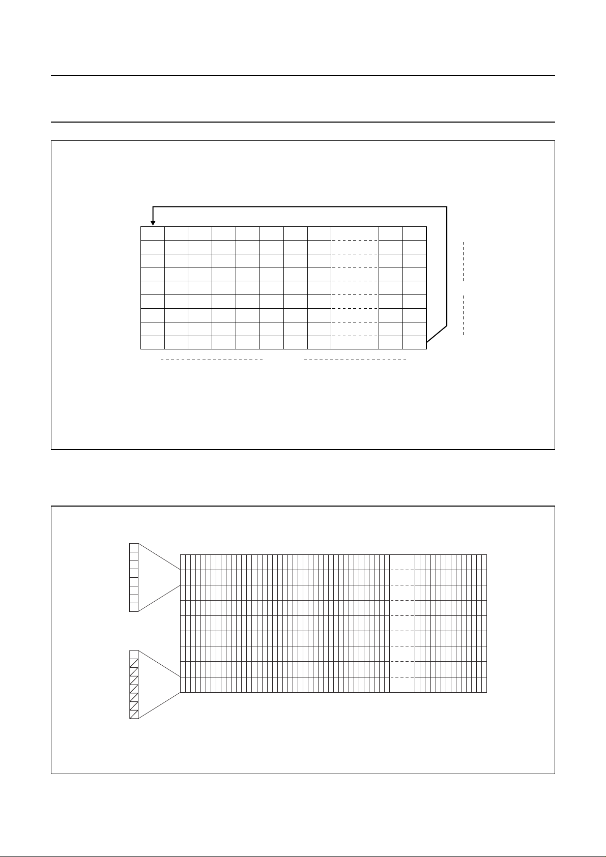
10 ADDRESSING
The Display Data RAM (DDRAM) of the PCF8548 is accessed as indicated in Figs 3, 6, 7, 8 and 9. The DDRAM has a
matrix of 65 × 102 bits. The RAM cells are addressed by the X and Y address pointers. The address ranges are X0 to
X101 (1100101b) and Y0 to Y8(1000b). Addressesoutside ofthese rangesare not allowed. In verticaladdressing mode
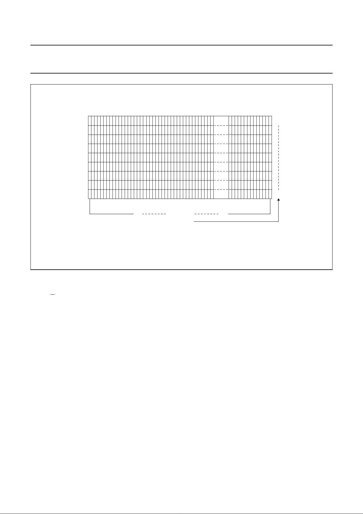
(V = 1) the Y address increments after each byte (see Fig.5). After the last Y address (Y = 8), Y wraps around to 0 and
X incrementsto addressthe nextcolumn. Inthe horizontaladdressing mode (V = 0)the X addressincrements aftereach
byte (see Fig.4). After thelast X address(X = 101), X wraps around to 0 andY increments toaddress thenext row. After
the very last address (X = 101 and Y = 8) the address pointers wrap around to address X = 0 andY=0.
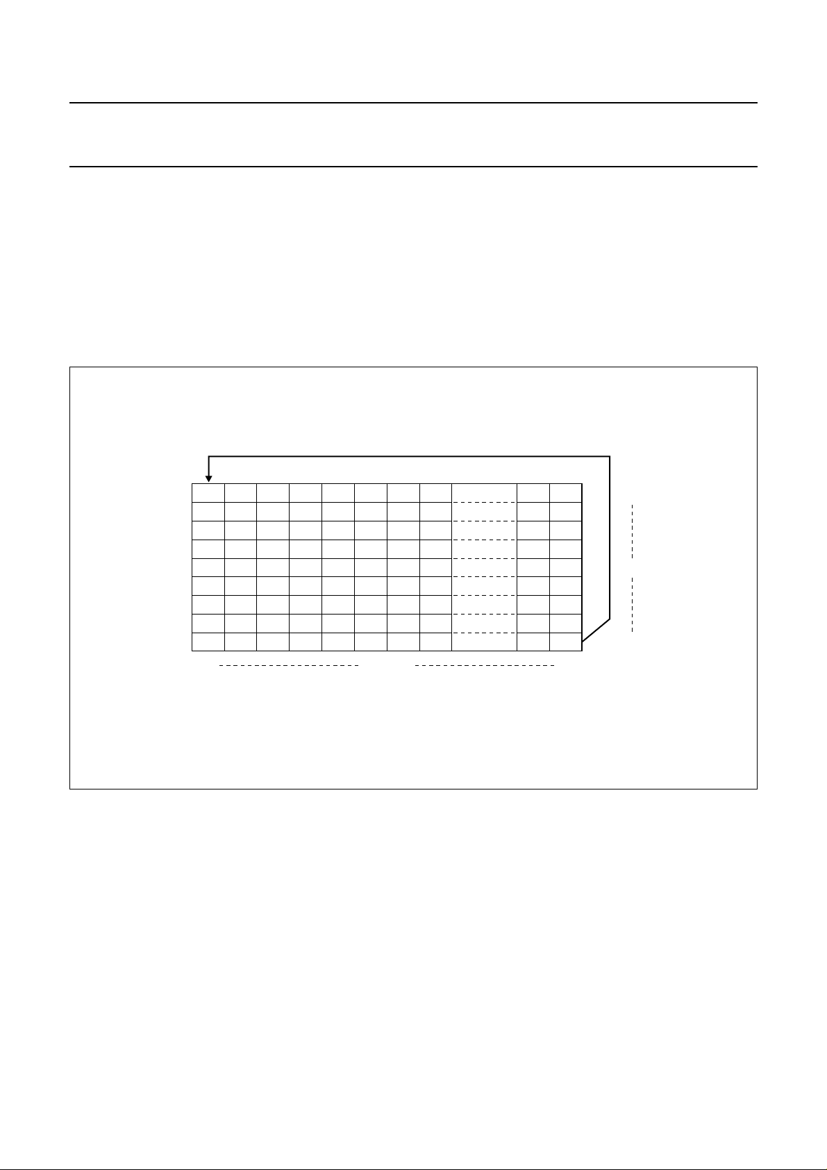
10.1 Display data RAM structure
handbook, full pagewidth
012
102 103 104
204 205 206
306 307 308
408 409 410
510 511 512
612 613 614
714 715 716
816 817 818
0 101X address
0
Y address
8917
MGS396
Fig.4 Sequence of writing data bytes into RAM with horizontal addressing (V = 0).
1999 Aug 16 9
Philips Semiconductors Product specification
65 × 102 pixels matrix LCD driver PCF8548
handbook, full pagewidth
09
110
2
3
4
5
6
7
8
0 101X address
0
Y address
8917
MGS397
Fig.5 Sequence of writing data bytes into RAM with vertical addressing (V = 1).
The DO bit defines the bit order (MSB on top or MSB on bottom) for writing to the RAM (see Figs 6 and 7).
handbook, full pagewidth
MSB
LSB
MSB
LSB
Fig.6 RAM byte organization, if DO = 0.
1999 Aug 16 10
MGS398

Philips Semiconductors Product specification
65 × 102 pixels matrix LCD driver PCF8548
handbook, full pagewidth
LSB
MSB
LSB
MGS399
MSB
Fig.7 RAM byte organization, if DO = 1.
The MX bit allows a horizontal mirroring; when MX = 1, the X address space is mirrored. The address X = 0 is then
located at the right side (column 101) of the display(see Fig.9). When MX = 0 the mirroringis disabled and the address
X = 0 is located at the left side (column 0) of the display (see Fig.8).
handbook, full pagewidth
0 101X address
Y address
Fig.8 RAM format addressing (MX = 0).
1999 Aug 16 11
0
8
MGS400
Philips Semiconductors Product specification
65 × 102 pixels matrix LCD driver PCF8548
handbook, full pagewidth
10.2 RAM access
101 0X address
Y address
Fig.9 RAM format addressing (MX = 1).
0
8
MBL044
If the D/C bit is logic 1 the RAM can be written to. The data is written to the RAM during the acknowledge cycle.
1999 Aug 16 12
 Loading...