

Philips PCF8535 Datasheet
INTEGRATED CIRCUITS
DATA SH EET
PCF8535
65 × 133 pixel matrix driver
Objective specification
File under Integrated Circuits, IC12
1999 Aug 24

Philips Semiconductors Objective specification
65 × 133 pixel matrix driver PCF8535
CONTENTS
1 FEATURES
2 APPLICATIONS
3 GENERAL DESCRIPTION
4 ORDERING INFORMATION
5 BLOCK DIAGRAM
5.1 Block diagram functions
5.1.1 Oscillator
5.1.2 Power-on reset
5.1.3 I2C-bus controller
5.1.4 Input filters
5.1.5 Display data RAM
5.1.6 Timing generator
5.1.7 Address counter
5.1.8 Display address counter
6 PINNING
6.1 Pin functions
6.1.1 R0 to R64
6.1.2 C0 to C132
6.1.3 V
6.1.4 V
6.1.5 V
6.1.6 V
6.1.7 V
and V
SS1
to V
DD1
LCDOUT
LCDIN
LCDSENSE
SS2
DD3
6.1.8 SDA
6.1.9 SDAOUT
6.1.10 SCL
6.1.11 SA0 and SA1
6.1.12 OSC
6.1.13 RES
6.1.14 T1, T2, T3, T4 and T5
7 FUNCTIONAL DESCRIPTION
7.1 Reset
7.2 Power-down
7.3 LCD voltage selector
7.4 Oscillator
7.5 Timing
7.6 Column driver outputs
7.7 Row driver outputs
7.8 Drive waveforms
7.9 Set multiplex rate
7.10 Bias system
7.10.1 Set bias system
7.11 Temperature measurement
7.11.1 Temperature read back
7.12 Temperature compensation
7.12.1 Temperature coefficients
7.13 V
OP
7.13.1 Set VOP value
7.14 Voltage multiplier control
7.14.1 S[1:0]
7.15 Addressing
7.15.1 Input addressing
7.15.2 Output addressing
7.16 Instruction set
7.16.1 RAM read/write command page
7.16.2 Function and RAM command page
7.16.3 Display setting command page
7.16.4 HV-gen command page
7.16.5 Special feature command page
7.16.6 Instruction set
7.17 I2C-bus interface
7.17.1 Characteristics of the I2C-bus
7.17.2 I2C-bus protocol
8 LIMITING VALUES (PROVISIONAL)
9 HANDLING
10 DC CHARACTERISTICS
11 AC CHARACTERISTICS
12 RESET TIMING
13 APPLICATION INFORMATION
14 BONDING PAD LOCATIONS
15 DEVICE PROTECTION DIAGRAM
16 TRAY INFORMATION
17 DEFINITIONS
18 LIFE SUPPORT APPLICATIONS
19 PURCHASE OF PHILIPS I2C COMPONENTS
20 BARE DIE DISCLAIMER
1999 Aug 24 2
Philips Semiconductors Objective specification
65 × 133 pixel matrix driver PCF8535
1 FEATURES
• Single-chip LCD controller/driver
• 65 row, 133 column outputs
• Display data RAM 65 × 133 bits
• 133 icons (last row is used for icons)
• Fast mode I2C-bus interface (400 kbits/s)
• Software selectable multiplex rates:
1:17,1:26,1:34,1:49and1:65
• On-chip:
– Generation of intermediate LCD bias voltages
– Oscillator requires no external components
(external clock also possible)
– Generation of V
LCD
.
• CMOS compatible inputs
• Software selectable bias configuration
• Logic supply voltage range V
• Supply voltage range for high voltage part V
V
DD3
to V
SS2
and V
4.5 to 5.5 V
SS3
• Display supply voltage range V
DD1
LCD
to V
to VSS:
4.5 to 5.5 V
SS1
DD2
and
– Mux rate 1 : 65: 8 to 16 V.
• Low power consumption, suitable for battery operated
systems
• Internal Power-on reset and/or external reset
• Temperature read back available
• Manufactured in N-well silicon gate CMOS process.
2 APPLICATIONS
• Automotive information systems
• Telecommunication systems
• Point-of-sale terminals
• Instrumentation.
3 GENERAL DESCRIPTION
The PCF8535 is a low power CMOS LCD row/column
driver, designed to drive dot matrix graphic displays at
multiplex rates of 1 : 17, 1 : 26, 1 : 34, 1 : 49 and 1 : 65.
Furthermore, it can drive up to 133 icons. All necessary
functions for the display are provided in a single chip,
including on-chip generation of LCD bias voltages,
resulting in a minimum of external components and low
power consumption. The PCF8535 is compatible with
most microcontrollers and communicates via an industry
standard two-line bidirectional I2C-bus serial interface.
All inputs are CMOS compatible.
4 ORDERING INFORMATION
PACKAGE
TYPE NUMBER
NAME DESCRIPTION VERSION
PCF8535U − chip with bumps in tray −
1999 Aug 24 3
Philips Semiconductors Objective specification
65 × 133 pixel matrix driver PCF8535
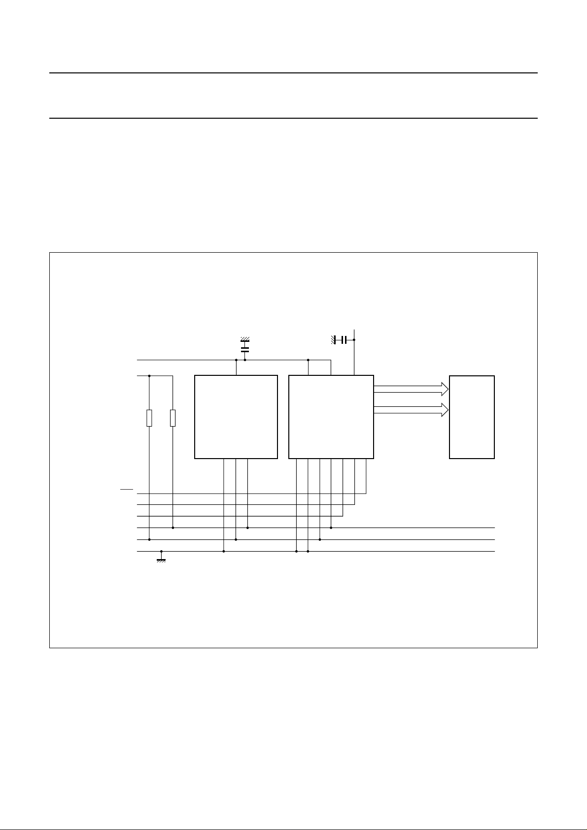
5 BLOCK DIAGRAM
handbook, full pagewidth
V
V
T4, T5
T1, T2, T3
V
LCDIN
V
LCDSENSE
V
LCDOUT
SDAOUT
SS1
SS2
SCL
SDA
BIAS
VOLTAGE
GENERATOR
V
LCD
GENERATOR
INPUT
FILTERS
R0 to R64
65
ROW
DRIVERS
PCF8535
C0 to C132
133
COLUMN
DRIVERS
DATA LATCHES
MATRIX
LATCHES
DISPLAY DATA RAM
MATRIX DATA
RAM
I2C-BUS
CONTROL
V
DD1
POWER-ON RESET
COMMAND
DECODER
V
DD2
INTERNAL
RESET
OSCILLATOR
TIMING
GENERATOR
DISPLAY
ADDRESS
COUNTER
ADDRESS
COUNTER
V
DD3
RES
OSC
SA0
SA1
Fig.1 Block diagram.
1999 Aug 24 4
MGS669

Philips Semiconductors Objective specification
65 × 133 pixel matrix driver PCF8535
5.1 Block diagram functions
5.1.1 OSCILLATOR The on-chip oscillator provides the display clock for the
system; it requires no externalcomponents. Alternatively,
an external display clock may be provided via the OSC
input. The OSC input must be connected to V
DD1
or V
SS1
when not in use. During power-down additional current
saving can be made if the external clock is disabled.
5.1.2 POWER-ON RESET The on-chip Power-on reset initializes the chip after
power-on or power failure.
2
5.1.3 I
C-BUS CONTROLLER
The I2C-bus controller detects the I2C-bus protocol, slave
address, commands and display data bytes. It performs
the conversion of the data input (serial-to-parallel).
The PCF8535 acts as an I2C-bus slave and therefore
cannot initiate bus communication.
5.1.4 INPUT FILTERS Input filters are provided to enhance noise immunity in
electrically adverse environments; RC low-pass filters are
provided on the SDA, SCL and RES lines.
5.1.5 D
ISPLAY DATA RAM
The PCF8535 contains a 65 × 133 bit static RAM which
storesthe display data. The RAM is dividedinto9 banks of
133 bytes. The last bank is used for icon data and is only
one bit deep. During RAM access, data is transferred to
the RAM via the I2C-bus interface. There is a direct
correspondence between the X address and the column
output number.
5.1.6 TIMING GENERATOR The timing generator produces the various signals
required to drive the internal circuitry. Internal chip
operation is not disturbed by operations on the data bus.
5.1.7 ADDRESS COUNTER TheAddressCounter(AC)sendsaddressestotheDisplay
Data RAM (DDRAM) for writing.
5.1.8 DISPLAY ADDRESS COUNTER The display is generated by continuously shifting rows of
RAM data to the dot matrix LCD via the column outputs.
The display status (all dots on or off, normal or inverse
video) is set via the I2C-bus.
1999 Aug 24 5

Philips Semiconductors Objective specification
65 × 133 pixel matrix driver PCF8535
6 PINNING
SYMBOL PAD DESCRIPTION
1 dummy pad
2 bump/alignment mark 1
R0 to R15 3 to 18 LCD row driver outputs
C0 to C132 19 to 151 LCD column driver outputs
R47 to R33 152 to 166 LCD row driver outputs
167 bump/alignment mark 2
168 dummy pad
R48 to R64 169 to 185 LCD row driver outputs; R64 is icon row
186 bump/alignment mark 3
187 to 189 dummy pad
OSC 190 oscillator
V
LCDIN
V
LCDOUT
V
LCDSENSE
RES 207 external reset input (active LOW)
T3 208 test output 3
T2 209 test output 2
T1 210 test output 1
V
DD2
V
DD3
V
DD1
SDA 230 and 231 I2C-bus serial data inputs
SDAOUT 232 I2C-bus serial data output
SA1 233 I2C-bus slave address input
SA0 234 I2C-bus slave address input
V
SS2
V
SS1
T5 251 test input 5
T4 252 test input 4
SCL 254 and 255 I2C-bus serial clock inputs
R32 to R16 257 to 273 LCD row driver outputs
191 to 196 LCD supply voltage
197 to 203 voltage multiplier output
204 voltage multiplier regulation input (V
205 and 206 dummy pad
211 to 218 supply voltage 2
219 to 222 supply voltage 3
223 to 228 supply voltage 1
229 dummy pad
235 to 242 ground 2
243 to 250 ground 1
253 dummy pad
256 bump/alignment mark 4
LCD
)
6.1 Pin functions
6.1.1 R0 TO R64
These pads output the display row signals.
1999 Aug 24 6
Philips Semiconductors Objective specification
65 × 133 pixel matrix driver PCF8535
6.1.2 C0 TO C132
These pads output the display column signals.
6.1.3 V
V
and V
SS1
6.1.4 V
V
is the logic supply. V
DD1
multiplier. For split power suppliesV
AND V
SS1
SS2
DD1
SS2
must be connected together.
TO V
DD3
and V
DD2
are for the voltage
DD3
and V
DD2
DD3
must be
connectedtogether.If only one supply voltage is available,
all three supplies must be connected together.
6.1.5 V
If, in the application, an external V
LCDOUT
is used, V
LCD
LCDOUT
must be left open-circuit; otherwise (if the internal voltage
multiplier is enabled) the chip may be damaged. V
should not be driven when V
is below its minimum
DD1
LCDOUT
allowed value otherwise a low impedance path between
V
LCDOUT
6.1.6 V
This is the V
If the internal V
V
LCDIN
driven when V
otherwisea low impedance path between V
and V
LCDIN
will exist.
SS1
supply for when an external V
LCD
generator is used, then V
LCD
must be connected together. V
is below its minimum allowed value,
DD1
should not be
LCDIN
LCDIN
is used.
LCD
LCDOUT
andV
and
SS1
will exist.
and the Indium Tin Oxide (ITO) track resistance. It is
possible that during the acknowledge cycle the PCF8535
will not be able to create a valid logic 0 level. By splitting
the SDA input from the SDAOUT output the device could
be used in a mode that ignores the acknowledge bit.
In COG applications where the acknowledge cycle is
required or where read back is required, it is necessary to
minimizethetrackresistancefromtheSDAOUT pad to the
system SDA line to guarantee a valid LOW level.
6.1.10 SCL
2
C-bus serial clock input.
I
6.1.11 SA0 AND SA1
Least significant bits of the I2C-bus slave address.
Table 1 Slave address; see note 1
SA1 AND SA0 MODE SLAVE ADDRESS
0 and 0 write 78H
read 79H
0 and 1 write 7AH
read 7BH
1 and 0 write 7CH
read 7DH
1 and 1 write 7EH
read 7FH
6.1.7 V
LCDSENSE
This is the input to the internal voltage multiplier regulator.
It must be connected to V
LCDOUT
when the internal voltage
generator is used otherwise it may be left open-circuit.
V
LCDSENCE
should not be driven when V
is below its
DD1
minimum allowed value, otherwise a low impedance path
between V
LCDSENCE
and V
will exist.
SS1
6.1.8 SDA I2C-bus serial data input.
6.1.9 SDAOUT SDAOUT is the serial data acknowledge for the I2C-bus.
By connecting SDAOUT to SDA externally, the SDA line
becomes fully I2C-bus compatible. Having the
acknowledge output separated from the serial data line is
advantageous in Chip-On-Glass (COG) applications.
In COG applications where the track resistance from the
SDAOUT pad to the system SDA line can be significant, a
potential divider is generated by the bus pull-up resistor
1999 Aug 24 7
Note
1. The slave address is a concatination of the following
bits {01111, SA1, SA0 and R/W}.
6.1.12 OSC
If the on-chip oscillator is used this input must be
connected to V
DD1
or V
SS1
.
6.1.13 RES
External reset pad: when this pad is LOW the chip will be
reset; see Section 7.1. If an external reset is not required,
this pad must be tied to V
. Timing for the RES pad is
DD1
given in Chapter 12.
6.1.14 T1, T2, T3, T4 AND T5
In applications T4 and T5 must be connected to VSS.
T1, T2 and T3 are to be left open-circuit.
Philips Semiconductors Objective specification
65 × 133 pixel matrix driver PCF8535
7 FUNCTIONAL DESCRIPTION
The PCF8535 is a low power LCD driver designed to interface with microprocessors/microcontrollers and a wide variety
of LCDs.
The host microprocessor/microcontroller and the PCF8535 are both connected to the I2C-bus. The SDA and SCL lines
must be connected to the positive power supply via pull-up resistors. The internal oscillator requires no external
components. The appropriate intermediate biasing voltage for the multiplexed LCD waveforms are generated on-chip.
The only other connections required to complete the system are to the power supplies (VDD,VSSand V
capacitors for decoupling V
LCD
and VDD.
) and suitable
LCD
handbook, full pagewidth
V
to V
DD1
V
DD(I2C)
V
SS1, VSS2
DD3
RES
SA0
SA1
SCL
SDA
V
LCD
DD2
DD1,VDD3
V
V
HOST
MICROPROCESSOR/
R
R
pu
pu
MICROCONTROLLER
V
SS
SS1VSS2
V
PCF8535
133 column drivers
65 row drivers
LCD PANEL
MGS670
Fig.2 Typical system configuration.
1999 Aug 24 8

Philips Semiconductors Objective specification
65 × 133 pixel matrix driver PCF8535
7.1 Reset
The PCF8535 has two reset modes; internal Power-on
reset or external reset. Reset initiated from either the RES
pad or the internal Power-on reset block will initialize the
chip to the following starting condition:
• Power-down mode (PD = 1)
• Horizontal addressing (V = 0); no mirror X or Y
(MX = 0 and MY = 0)
• Display blank (D = 0 andE=0)
• Address counter X[6:0] = 0, Y[2:0] = 0 and XM0=0
• Bias system BS[2:0] = 0
• Multiplex rate M[2:0] = 0 (Mux rate1:17)
• Temperature control mode TC[2:0] = 0
• HV-gen control, HVE = 0 the HV generator is switched
off, PRS = 0 and S[1:0] = 00
• V
LCDOUT
is equal to 0 V
• RAM data is unchanged (Note: RAM data is undefined
after power-up)
• All row and column outputs are set to VSS (display off)
• TRS and BRS are set to zero
• Direct mode is disabled (DM = 0)
• Internal oscillator is selected, but not running (EC = 0)
• Bias current set to low current mode (IB = 0).
7.3 LCD voltage selector
The practical value for VOP is determined by equating
V
with defined LCD threshold voltage (Vth), typically
off(rms)
when the LCD exhibits approximately 10% contrast.
7.4 Oscillator
The internal logic operation and the multi-level drive
signals of the PCF8535 are clocked by the built-in RC
oscillator. No external components are required.
7.5 Timing
ThetimingofthePCF8535organizestheinternaldataflow
of the device. The timing also generates the LCD frame
frequency which is derived from the clock frequency
generated in the internal clock generator.
7.6 Column driver outputs
The LCD drive section includes 133 column outputs
(C0 to C132) which should be connected directly to the
LCD. The column output signals are generated in
accordance with the multiplexed row signals and with the
data in the display latch. When less than 133 columns are
required the unused column outputs should be left
open-circuit.
7.7 Row driver outputs
7.2 Power-down
During power-down all static currents are switched off (no
internal oscillator, no timing and no LCD segment drive
system) and all LCD outputs are internally connected to
VSS. The serial bus function remains active.
The LCD drive section includes 65 row outputs
(R0 to R64) which should be connected directly to the
LCD. The row output signals are generated in accordance
with the selected LCD drive mode. If lower Mux rates or
less than 65 rows are required, the unused outputs should
be left open-circuit.
1999 Aug 24 9
Philips Semiconductors Objective specification
65 × 133 pixel matrix driver PCF8535
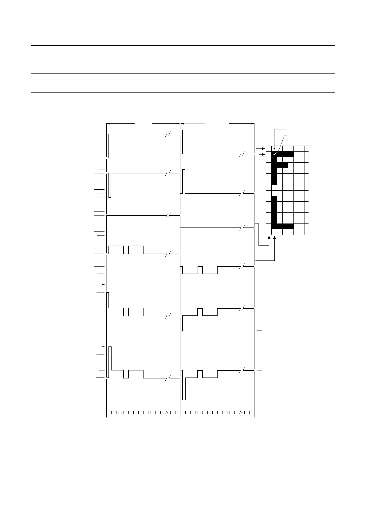
7.8 Drive waveforms
ROW 0
R0 (t)
ROW 1
R1 (t)
COL 0
C0 (t)
COL 1
C1 (t)
V
LCD
V3 − V
V
V
V
V
V
V
V
V
V
V
V
V
V
V
V
V
V
V
V
V
V
V
V
V
LCD
2
3
4
5
SS
LCD
2
3
4
5
SS
LCD
2
3
4
5
SS
LCD
2
3
4
5
SS
− V
SS
SS
frame n frame n + 1
V
state1
V
state2
(t)
(t)
V
− V
LCD
V
V
V
(t) = C1(t) − R0(t).
state1
V
(t) = C1(t) − R1(t).
state2
state1
state2
(t)
(t)
0 V
V3 − V
V
LCD
V3 − V
V
LCD
0 V
V3 − V
2
SS
− V
SS
SS
− V
2
SS
012345678... ... 64 01234567 8... ... 64
Fig.3 Typical LCD driver waveforms.
1999 Aug 24 10
V4 − V
0 V
VSS − V
V4 − V
V
− V
SS
V4 − V
0 V
VSS − V
V4 − V
V
− V
SS
MGS671
5
5
LCD
LCD
5
5
LCD
LCD
Philips Semiconductors Objective specification
65 × 133 pixel matrix driver PCF8535
7.9 Set multiplex rate
The PCF8535 can be used to drive displays of varying sizes. The multiplex mode selected controls which rows are used.
In all cases, the last row is always driven and is intended for icons. If Top Row Swap (TRS) is at logic 1 then the icon row
will be output on pad R48. M[2:0] selects the multiplex rate (see Table 2).
Table 2 Multiplex rates
M[2] M[1] M[0] MULTIPLEX RATE ACTIVE ROWS
0 0 0 1 : 17 R0 to R15 and R64
0 0 1 1 : 26 R0 to R24 and R64
0 1 0 1 : 34 R0 to R32 and R64
0 1 1 1 : 49 R0 to R47 and R64
1 0 0 1:65 R0toR64
101 − 111 do not use −
7.10 Bias system
7.10.1 SET BIAS SYSTEM
The bias voltage levels are set in the ratio of R − R − nR − R − R. Differentmultiplex rates require differentfactors n. This
is programmed by BS[2:0]. For optimum bias values, n can be calculated from:
n Mux rate 3–=
Changing the bias system from the optimum will have a consequence on the contrast and viewing angle. One reason to
come away from the optimum would be to reduce the required V
. A compromise between contrast and VOP must be
OP
found for any particular application.
Table 3 Programming the required bias system
BS[2] BS[1] BS[0] n BIAS MODE TYPICAL MUX RATES
00071/
00161/
01051/
01141/
10031/
10121/
11011/
1110
11
10
9
8
7
6
5
1
/
4
1 : 100
1:80
1:65
1:49
1:33
1:26
1:17
1:9
1999 Aug 24 11

Philips Semiconductors Objective specification
65 × 133 pixel matrix driver PCF8535
Table 4 Example of LCD bias voltage for1/7bias, n = 3
1
SYMBOL BIAS VOLTAGE FOR
V1 V
V2
V3
V4
V5
V6 V
6
/7× V
5
/7× V
2
/7× V
1
/7× V
LCD
SS
/7BIAS
LCD
LCD
LCD
LCD
7.11 Temperature measurement
7.11.1 T
EMPERATURE READ BACK
The PCF8535 has an in-built temperature sensor.
For power saving, the sensor should only be enabled
when a measurement is required. It will not operate in
power-down mode. The temperature read back requires a
clock to operate. Normally the internal clock is used but, if
the device is operating from an external clock, then this
must be present for the measurement to work. V
V
mustalso be applied. A measurement is initialized by
DD3
DD2
and
setting the SM bit. Once started the SM bit will be
automatically cleared. An internal oscillator will be
initialized and allowed to warm-up for approximately
2 frame periods. After this the measurement starts and
lasts for a maximum of 2 frame periods.
Temperature data is returned via a status register. During
the measurement the register will contain zero. Once the
measurement is completed the register will be updated
with the current temperature (non zero value). Because
the I2C-bus interface is asynchronous to the temperature
measurement, read back prior to the end of the
measurement is not guaranteed. If this mode is required
the register should be read twice to validate the data.
For calibrating the temperature read-out a measurement
must be taken at a defined temperature. The offset
between the ideal read-out and the actual result has to be
stored into a non-volatile register (e.g. EEPROM);
Offset TR
where TR
meas
TR
–=
ideal
meas
is the actual temperature read-out of the
(2)
PCF8535.
The calibrated temperature read-out can be calculated for
each measurement as follows:
TR
cal
TR
meas
Offset+=
(3)
The accuracy after the calibration is ±6.7% (plus ±1 lsb) of
the difference between the current temperature and the
calibration temperature. For this reason a calibration at or
near the most sensitive temperature for the display is
recommended.
E.g. for a calibration at 25 °C with the current temperature
at −20 °C, the absolute error may be calculated as:
Absolute error = 0.067 × (25 °C −−20 °C)
= ±3 °C+±1 lsb = ±4.17 °C.
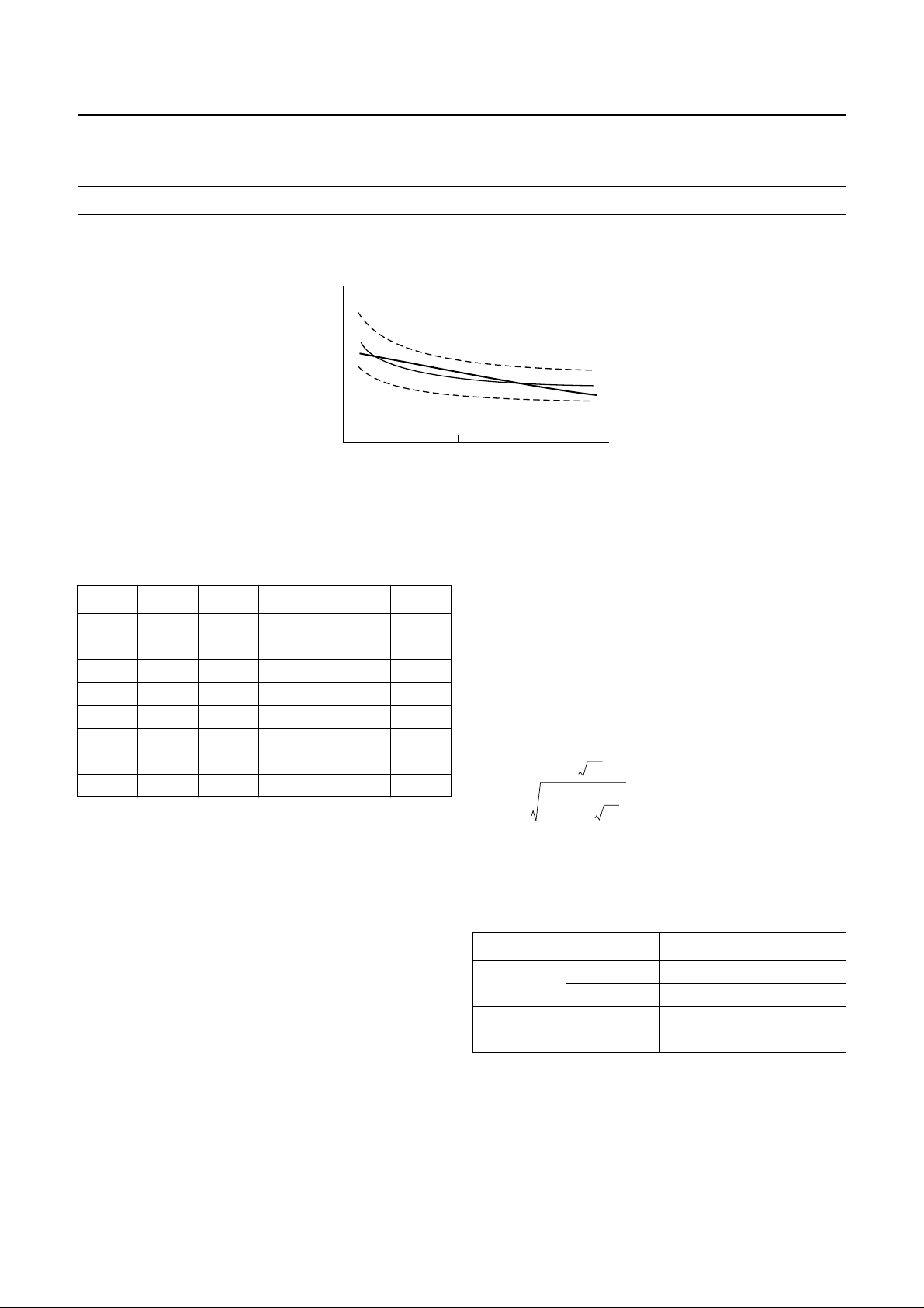
7.12 Temperature compensation
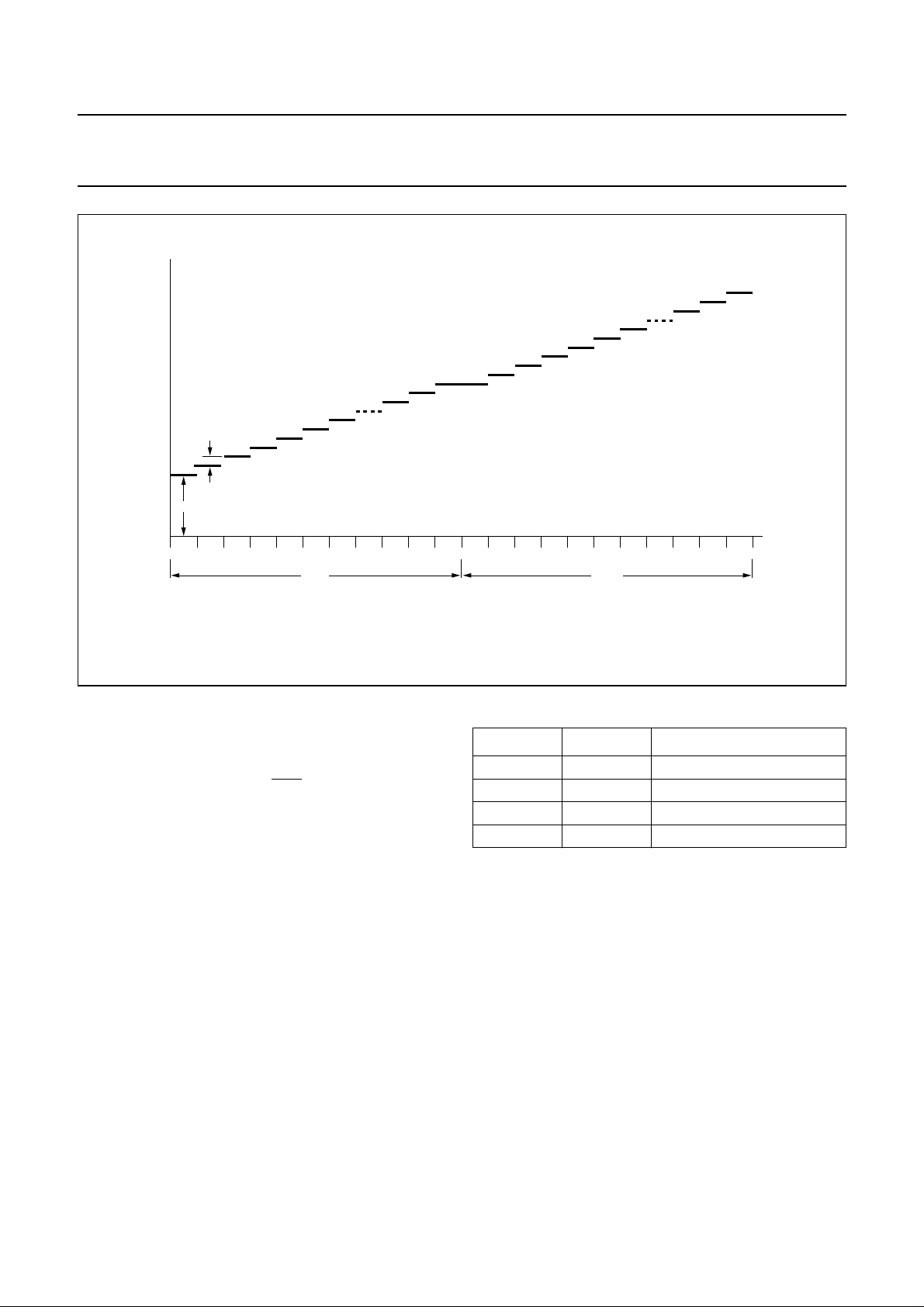
7.12.1 TEMPERATURE COEFFICIENTS Due to the temperature dependency of the liquid crystals
viscosity the LCD controlling voltage,V must be increased
at lower temperatures to maintain optimum contrast.
Figure 4 shows V
as a function of temperature for a
LCD
typical high multiplex rate liquid.
Inthe PCF8535 the temperature coefficient of V
LCD
canbe
selected from 8 values by setting bits TC[2:0],
see Table 5.
The ideal temperature read-out can be calculated as
follows;
TR
128 T 27 °C–()
ideal
×+=
-- c
(1)
1
where T is the on-chip temperature in °C and c is the
conversion constant; c = 1.17 °C/lsb.
Toimprove the accuracy of the temperature measurement
a calibration is recommended during the assembly of the
final product.
1999 Aug 24 12
Philips Semiconductors Objective specification
65 × 133 pixel matrix driver PCF8535
handbook, halfpage
V
LCD
Fig.4 V
as function of liquid crystal temperature (typical values).
LCD
Table 5 Selectable temperature coefficients
TC[2] TC[1] TC[0] TC VALUE UNIT
000 0 1/°C
001−0.44 × 10
010−1.10 × 10
011−1.45 × 10
100−1.91 × 10
101−2.15 × 10
110−2.32 × 10
111−2.74 × 10
7.13 V
7.13.1 SET V
OP
OP
VALUE
−3
−3
−3
−3
−3
−3
−3
1/°C
1/°C
1/°C
1/°C
1/°C
1/°C
1/°C
The voltage at the reference temperature can be
calculated as: [V
V
LCD
Tcut()
The operating voltage, V
(T=T
LCD
aVOPb×+()=
)]
cut
, can be set by software.
OP
(4)
The generated voltage is dependent on the temperature,
programmed Temperature Coefficient (TC) and the
programmed voltage at the reference temperature (T
V
LCD
aVOPb×+()1TT
The values for T
, a and b are given in Table 6.
cut
–()TC×()+()×=
cut
cut
):
(5)
The maximumvoltagethatcan be generated is dependent
on the voltage V
and the display load current.
DD2
Two overlapping VOP ranges are selectable via the
command page “Hv-gen control”, see Fig.5.
MGS473
0 °C
T
The low range offers programming from 4.5 to 10.215 V,
with the high range from 10.215 to 15.93 V at the cut point
temperature, T
. Care must be taken, when using
cut
temperature coefficients, that the programmed voltage
does not exceed the maximum allowed V
LCD
voltage,
see Chapter 10.
Fora particular liquid, the optimumV
canbe calculated
LCD
for a given multiplex rate. For a Mux rate of 1 : 65, the
optimum operating voltage of the liquid can be calculated
as:
V
LCD
where V
165+
---------------------------------------
×
–
21
is the threshold voltage of the liquid crystal
th
----------
1
65
V
× 6.85 Vth×==
th
material used.
Table 6 Values for parameters of the HV generator
programming
SYMBOL BITS VALUE UNIT
a PRS = 0 4.5 V
PRS = 1 10.215 V b 0.045 V T
cut
27 °C
(6)
1999 Aug 24 13
Philips Semiconductors Objective specification
65 × 133 pixel matrix driver PCF8535
handbook, full pagewidth
V
LCD
b
a
00 01 02
VOP[6:0] programming (00H to 7FH, programming range LOWand HIGH).
03 04 05 06 . . . 5F 6F 7F 00 01 02 03 04 05 06 . . . 5F 6F 7F
LOW HIGH
Fig.5 VOP programming of PCF8535.
7.14 Voltage multiplier control
7.14.1 S[1:0] The PCF8535 incorporates a software configurable
voltage multiplier. After reset (RES) the voltage multiplier
is set to 2 × V
. Other voltage multiplier factors are set
DD2
via the HV-gen command page. Before switching on the
charge pump, the charge pump has to be pre-charged
using the following sequence.
A starting state of HVE = 0, DOF = 0, PD = 1 and DM = 0
is assumed. A small delay between steps is indicated.
The recommended wait period is 20 µs per 100 nF of
capacitance on V
LCD1
.
1. Set DM = 1 and PD = 0
2. Delay
3. Set the multiplication factor to 2 by setting S[1:0] = 00
4. Set the required VOP and PRS.
5. Set HVE = 1 to switch-on the charge pump with a
multiplication factor of 2
6. Delay
7. Increase the number of stages, one at a time, with a
delay between each until the required level is
achieved.
MGS472
Table 7 HV generator multiplication factor
S[1] S[0] MULTIPLICATION FACTOR
00 2× V
01 3× V
10 4× V
11 5× V
DD2
DD2
DD2
DD2
1999 Aug 24 14
Philips Semiconductors Objective specification
65 × 133 pixel matrix driver PCF8535
7.15 Addressing
Addressing of the RAM can be split into two parts; input
addressing and output addressing. Input addressing is
concerned with writing data into the RAM. Output
addressing is almost entirely automatic and taken care of
by the device, however, it is possible to affect the output
mode.
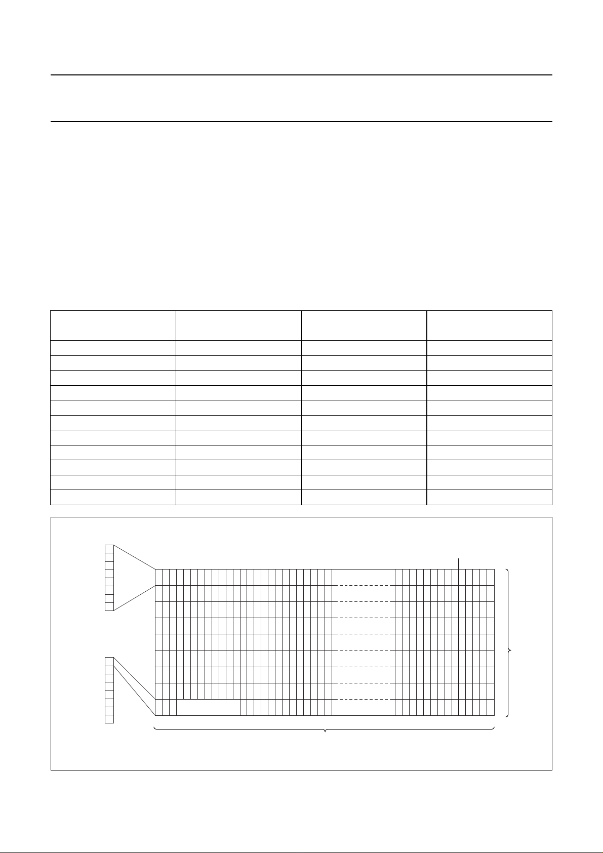
7.15.1 INPUT ADDRESSING
Data is down loaded byte wise into the RAM matrix of the
PCF8535 as indicated in Figs 6 to 10.
Table 8 Effect of X-RAM page pointer
X ADDRESS POINTER
X-RAM PAGE POINTER
XM
0
0 0 C0 C132 1 0 C1 C131 2 0 C2 C130
:::: 125 0 C125 C7 126 0 C126 C6 127 0 C127 C5
0 1 C128 C4 1 1 C129 C3
::::
4 1 C132 C0
The display RAM has a matrix of 65 × 133 bits.
The columns are addressed by a combination of the
X address pointer and the X-RAM page pointer, whilst the
rows addressed in groups of 8 by the Y address pointer.
The X address pointer has a range of 0 to 127 (7FH).
Its range can be extended by the X-RAM page pointer,
XM0. The Y address pointer has a range of 0 to 8 (08H).
The PCF8535 is limited to 133 columns by 65 rows,
addressing the RAM outside of this area is not allowed.
ADDRESSED COLUMN
MX = 0
ADDRESSED COLUMN
MX = 1
Banks 1 to 7 use
the entire byte
handbook, full pagewidth
MSB
LSB
Bank 8 is only
1 bit deep and
uses the MSB
MSB
LSB
01234
icon data
56789
101112131415161718192021222324
Fig.6 RAM format, input addressing.
1999 Aug 24 15
.. .. .. ..
X address
XM0 = 1XM0 = 0
0
1
2
3
4
5
Y address
6
7
8
119
123
120
121
122
124
125
126
127
01234
MGS673
Philips Semiconductors Objective specification
65 × 133 pixel matrix driver PCF8535
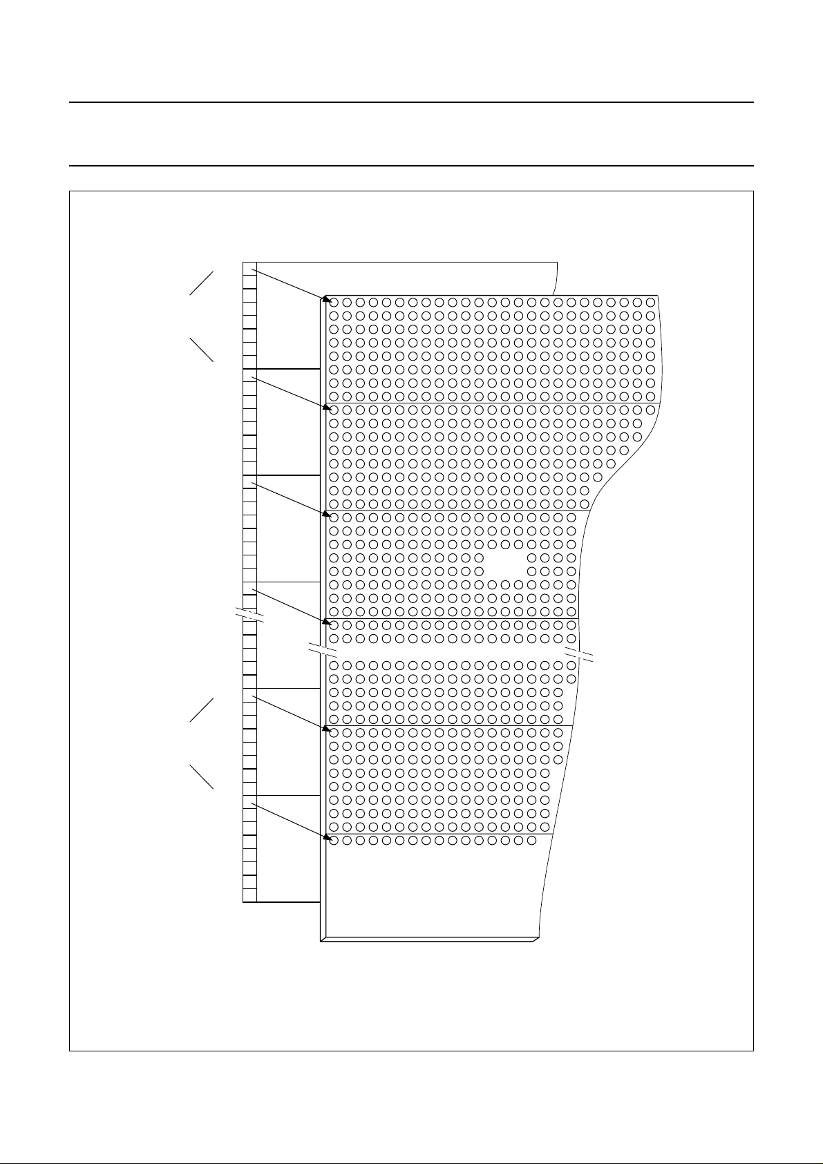
Data byte in location
X = 0, Y = 0, MX0 = 0
(MX = 0, MY = 0)
MSB
LSB
bank 0
top of LCD
R0
bank 1
R8
bank 2
R16
LCD
bank 3
R24
MSB
Data byte in location
Y = 7, X = 0, MX0 = 0
(MX = 0, MY = 0)
LSB
bank 7
bank 8
Fig.7 DDRAM to display mapping.
1999 Aug 24 16
R56
R64
MGS674
 Loading...