

Philips PCF8533U-2-F2, PCF8533U-2-2, PCF8533U-2-F1 Datasheet

DATA SH EET
Product specification
Supersedes data of 1999 Mar 12
File under Integrated Circuits, IC12
1999 Jul 30
INTEGRATED CIRCUITS
PCF8533
Universal LCD driver for low
multiplex rates

1999 Jul 30 2
Philips Semiconductors Product specification
Universal LCD driver for low multiplex rates PCF8533
CONTENTS
1 FEATURES
2 GENERAL DESCRIPTION
3 ORDERING INFORMATION
4 BLOCK DIAGRAM
5 PINNING
6 FUNCTIONAL DESCRIPTION
6.1 Power-on reset
6.2 LCD bias generator
6.3 LCD voltage selector
6.4 LCD drive mode waveforms
6.4.1 Static drive mode
6.4.2 1 : 2 multiplex drive mode
6.4.3 1 : 3 multiplex drive mode
6.4.4 1 : 4 multiplex drive mode
6.5 Oscillator
6.5.1 Internal clock
6.5.2 External clock
6.6 Timing
6.7 Display register
6.8 Segment outputs
6.9 Backplane outputs
6.10 Display RAM
6.11 Data pointer
6.12 Subaddress counter
6.13 Output bank selector
6.14 Input bank selector
6.15 Blinker
7 CHARACTERISTICS OF THE I2C-BUS
7.1 Bit transfer
7.2 START and STOP conditions
7.3 System configuration
7.4 Acknowledge
7.5 PCF8533 I2C-bus controller
7.6 Input filters
7.7 I2C-bus protocol
7.8 Command decoder
7.9 Display controller
7.10 Cascaded operation
8 LIMITING VALUES
9 HANDLING
10 DC CHARACTERISTICS
11 AC CHARACTERISTICS
12 BONDING PAD LOCATIONS
13 DEVICE PROTECTION
14 TRAY INFORMATION
15 DEFINITIONS
16 LIFE SUPPORT APPLICATIONS
17 PURCHASE OF PHILIPS I2C COMPONENTS
18 BARE DIE DISCLAIMER

1999 Jul 30 3
Philips Semiconductors Product specification
Universal LCD driver for low multiplex rates PCF8533
1 FEATURES
• Single-chip LCD controller/driver
• Selectable backplanedrive configuration: static or 2/3/4
backplane multiplexing
• Selectable display bias configuration: static,1⁄2or1⁄
3
• Internal LCD bias generation with voltage-follower
buffers
• 80 segment drives: up to forty 8-segment numeric
characters; up to twentyone 15-segment alphanumeric
characters; or any graphics of up to 320 elements
• 80 × 4-bit RAM for display data storage
• Auto-incremented display data loading across device
subaddress boundaries
• Display memory bank switching in static and duplex
drive modes
• Versatile blinking modes
• LCD and logic supplies may be separated
• Wide power supply range: from 1.8 to 5.5 V
• Wide LCD supply range: from 2.5 V for low threshold
LCDs and up to 6.5 V for guest-host LCDs and high
threshold (automobile) twisted nematic LCDs
• Low power consumption
• 400 kHz I2C-bus interface
• TTL/CMOS compatible
• Compatible with 4-bit, 8-bit or 16-bit
microprocessors/microcontrollers
• May be cascaded for large LCD applications (up to
5120 segments possible)
• No external components
• Compatible with Chip-On-Glass (COG) technology
• Manufactured in silicon gate CMOS process.
2 GENERAL DESCRIPTION
The PCF8533 is a peripheral device which interfaces to
almost any Liquid Crystal Display (LCD) with low multiplex
rates. It generates the drive signals for any static or
multiplexed LCD containing up to four backplanes and up
to80 segmentsandcaneasily be cascaded for larger LCD
applications. The PCF8533 is compatible with most
microprocessors/microcontrollersandcommunicatesvia a
two-line bidirectional I2C-bus. Communication overheads
are minimized by a display RAM with auto-incremented
addressing, by hardware subaddressing and by display
memory switching (static and duplex drive modes).
3 ORDERING INFORMATION
TYPE NUMBER
PACKAGE
NAME DESCRIPTION VERSION
PCF8533U − chip with bumps in tray −
1999 Jul 30 4
Philips Semiconductors Product specification
Universal LCD driver for low multiplex rates PCF8533
This text is here in white to force landscape pages to be rotated correctly when browsing through the pdf in the Acrobat reader.This text is here in
_white to force landscape pages to be rotated correctly when browsing through the pdf intheAcrobatreader.This text is here inThis text is here in
white to forcelandscape pages to be rotated correctlywhen browsing through the pdf inthe Acrobat reader. white to forcelandscape pages to be ...
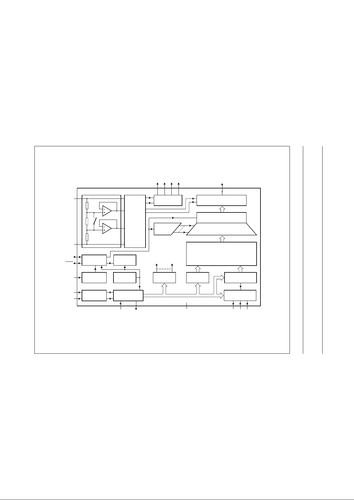
4 BLOCK DIAGRAM
Fig.1 Block diagram.
handbook, full pagewidth
MGL743
LCD
VOLTAGE
SELECTOR
CLOCK SELECT
AND TIMING
BLINKER
TIMEBASE
OSCILLATOR
INPUT
FILTERS
I
2
C-BUS
CONTROLLER
POWER-ON
RESET
CLK
SYNC
OSC
SCL
SDA
SA0
BACKPLANE
OUTPUTS
DISPLAY
CONTROL
BP0 BP1 BP2 BP3
DISPLAY SEGMENT OUTPUTS
DISPLAY REGISTER
OUTPUT BANK SELECT
AND BLINK CONTROL
80
S0 to S79
SDAACK V
DD
A0 A1 A2
PCF8533
LCD BIAS
GENERATOR
V
SS
V
LCD
COMMAND
DECODE
WRITE DATA
CONTROL
DISPLAY
RAM
DATA POINTER AND
AUTO INCREMENT
SUBADDRESS
COUNTER
1999 Jul 30 5
Philips Semiconductors Product specification
Universal LCD driver for low multiplex rates PCF8533
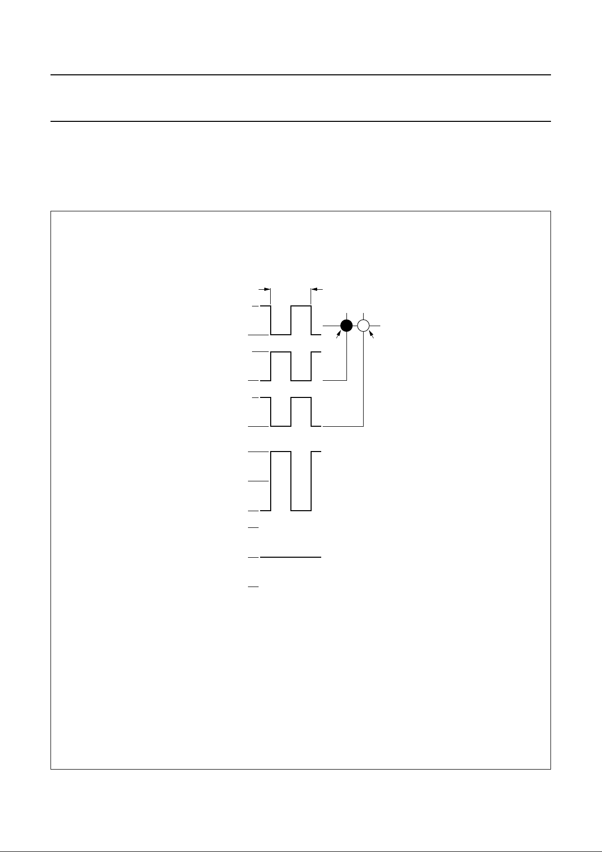
5 PINNING
Note
1. For most applications SDA and SDAACK will be shorted together; see Chapter 7.
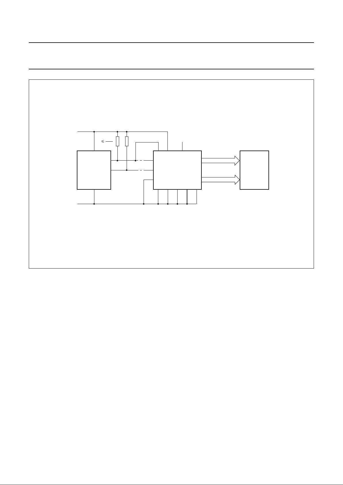
6 FUNCTIONAL DESCRIPTION
The PCF8533 is a versatile peripheral device designed to interface any microprocessor/microcontroller to a wide variety
of LCDs. It can directly drive any static or multiplexed LCD containing up to four backplanes and up to 80 segments.
The display configurations possible with the PCF8533 depend on the number of active backplane outputs required; a
selection of display configurations is given in Table 1.
All of the display configurations given in Table 1 can be implemented in the typical system shown in Fig.2.
The host microprocessor/microcontroller maintains the 2-line I
2
C-bus communication channel with the PCF8533.
The internal oscillator is selected by connecting pad OSC to VSS. The appropriate biasing voltages for the multiplexed
LCD waveforms are generated internally. The only other connections required to complete the system are to the power
supplies (VDD, VSSand V
LCD
) and the LCD panel selected for the application.
Table 1 Selection of display configurations
SYMBOL PAD DESCRIPTION
SDAACK 1 I2C-bus acknowledge output; note 1
SDA 2 and 3 I
2
C-bus serial data input; note 1
SCL 4 and 5 I
2
C-bus serial clock input
CLK 6 external clock input/output
V
DD
7 supply voltage
SYNC 8 cascade synchronization input/output
OSC 9 internal oscillator enable input
A0, A1 and A2 10, 11 and 12 subaddress inputs
SA0 13 I
2
C-bus slave address input; bit 0
V
SS
14 logic ground
V
LCD
15 LCD supply voltage
BP0, BP1, BP2 and BP3 17, 99, 16 and 98 LCD backplane outputs
S0 to S79 18 to 97 LCD segment outputs
NUMBER OF 7-SEGMENTS NUMERIC
14-SEGMENTS
ALPHANUMERIC
DOT MATRIX
BACKPLANES SEGMENTS DIGITS
INDICATOR
SYMBOLS
CHARACTERS
INDICATOR
SYMBOLS
4 320 40 40 20 40 320 dots (4 × 80)
3 240 30 30 16 16 240 dots (3 × 80)
2 160 20 20 10 20 160 dots (2 × 80)
1 80 10 10 5 10 80 dots (1 × 80)
1999 Jul 30 6
Philips Semiconductors Product specification
Universal LCD driver for low multiplex rates PCF8533
Fig.2 Typical system configuration.
handbook, full pagewidth
HOST
MICRO-
PROCESSOR/
MICRO-
CONTROLLER
R
t
r
2C
B
SDA
SDAACK
SCL
OSC
80 segment drives
4 backplanes
LCD PANEL
(up to 320
elements)
PCF8533
A0 A1 A2 SA0
V
DD
V
SS
V
SS
V
DD
V
LCD
MGL744
1999 Jul 30 7
Philips Semiconductors Product specification
Universal LCD driver for low multiplex rates PCF8533
6.1 Power-on reset
At Power-on the PCF8533 resets to a starting condition as
follows:
1. All backplane outputs are set to V
LCD
.
2. All segment outputs are set to V
LCD
.
3. Thedrivemode ‘1 : 4 multiplex with1⁄3bias’ is selected.
4. Blinking is switched off.
5. Input and output bank selectors are reset (as defined
in Table 5).
6. The I2C-bus interface is initialized.
7. The data pointer and the subaddress counter are
cleared.
8. Display disabled.
Data transfers on the I2C-bus should be avoided for 1 ms
following Power-on to allow completion of the reset action.
6.2 LCD bias generator
Fractional LCD biasing voltages are obtained from an
internal voltage divider of the three series resistors
connectedbetween V
LCD
andVSS.The centre resistor can
be switched out of the circuit to provide a1⁄2bias voltage
level for the 1 : 2 multiplex configuration.
6.3 LCD voltage selector
The LCD voltage selector co-ordinates the multiplexing of
the LCD in accordance with the selected LCD drive
configuration. The operation of the voltage selector is
controlled by MODE SET commands from the command
decoder.
The biasing configurations that apply to the preferred
modes of operation, together with the biasing
characteristics as functions of VOP and the resulting
discrimination ratios (D), are given in Table 2.
ApracticalvalueforVOPisdeterminedbyequatingV
off(rms)
with a defined LCD threshold voltage (Vth), typically when
the LCD exhibits approximately 10% contrast. In the static
drive mode a suitable choice is VOP>3Vth.
Multiplex drive ratios of 1 : 3 and 1 : 4 with
1
⁄2bias are
possible but the discrimination and hence the contrast
ratios are smaller ( = 1.732 for 1 : 3 multiplex or
= 1.528 for 1 : 4 multiplex).
The advantage of these modes is a reduction of the LCD
full-scale voltage V
OP
as follows:
• 1 : 3 multiplex (
1
⁄2bias):
• 1 : 4 multiplex (
1
⁄2bias):
These compare with V
OP
=3V
off(rms)
when1⁄3bias is used.
Note: VOP=V
LCD
.
3
21
3
----------
V
OP
6V
off(rms)
× 2.449V
off(rms)
==
V
OP
43×()
3
--------------------- -
2.309V
off(rms)
==
Table 2 Preferred LCD drive modes: summary of characteristics
LCD DRIVE MODE
NUMBER OF
LCD BIAS
CONFIGURATION
BACKPLANES LEVELS
static 1 2 static 0 1 ∞
1:2 2 3
1
⁄
2
0.354 0.791 2.236
1:2 2 4
1
⁄
3
0.333 0.745 2.236
1:3 3 4
1
⁄
3
0.333 0.638 1.915
1:4 4 4
1
⁄
3
0.333 0.577 1.732
V
off(rms)
V
OP
-------------------
V
on(rms)
V
OP
-------------------
D
V
on(rms)
V
off(rms)
-------------------
=
1999 Jul 30 8
Philips Semiconductors Product specification
Universal LCD driver for low multiplex rates PCF8533
6.4 LCD drive mode waveforms
6.4.1 STATIC DRIVE MODE
The static LCD drive mode is used when a single backplane is provided in the LCD. Backplane and segment drive
waveforms for this mode are shown in Fig.3.
Fig.3 Static drive mode waveforms.
V
state1
(t)=Vsn(t) − V
BP0
(t).
V
on(rms)=VLCD
.
V
state2
(t)=V
sn +1
(t) − V
BP0
(t).
V
off(rms)
=0V.
handbook, full pagewidth
MGL745
V
SS
V
LCD
V
SS
V
LCD
V
SS
V
LCD
V
LCD
−V
LCD
−V
LCD
V
LCD
state 1 0 V
BP0
S
n
Sn + 1
state 2 0 V
(a) Waveforms at driver.
(b) Resultant waveforms
at LCD segment.
LCD segments
state 1
(on)
state 2
(off)
T
frame

1999 Jul 30 9
Philips Semiconductors Product specification
Universal LCD driver for low multiplex rates PCF8533
6.4.2 1 : 2 MULTIPLEX DRIVE MODE
When two backplanes are provided in the LCD, the 1 : 2 multiplex mode applies. The PCF8533 allows the use of1⁄2bias
or1⁄3bias in this mode as shown in Figs 4 and 5.
Fig.4 Waveforms for the 1 : 2 multiplex drive mode with1⁄2bias.
V
state1
(t)=Vsn(t) − V
BP0
(t).
V
on(rms)
= 0.791V
LCD
.
V
state2
(t)=Vsn(t) − V
BP1
(t).
V
off(rms)
= 0.354V
LCD
.
handbook, full pagewidth
MGL746
state 1
BP0
(a) Waveforms at driver.
(b) Resultant waveforms
at LCD segment.
LCD segments
state 2
BP1
state 2
state 1
V
SS
V
LCD
V
LCD
/2
V
SS
V
SS
V
LCD
V
LCD
V
SS
V
LCD
V
LCD
V
LCD
0 V
0 V
V
LCD
/2
V
LCD
/2
V
LCD
/2
−V
LCD
−V
LCD
−V
LCD
/2
−V
LCD
/2
S
n
Sn + 1
T
frame

1999 Jul 30 10
Philips Semiconductors Product specification
Universal LCD driver for low multiplex rates PCF8533
Fig.5 Waveforms for the 1 : 2 multiplex drive mode with1⁄3bias.
V
state1
(t)=Vsn(t) − V
BP0
(t).
V
on(rms)
= 0.745V
LCD
.
V
state2
(t)=Vsn(t) − V
BP1
(t).
V
off(rms)
= 0.333V
LCD
.
handbook, full pagewidth
MGL747
state 1
BP0
(a) Waveforms at driver.
(b) Resultant waveforms
at LCD segment.
LCD segments
state 2
BP1
state 1
state 2
V
SS
V
LCD
2V
LCD
/3
V
LCD
/3
V
SS
V
LCD
2V
LCD
/3
V
LCD
/3
V
SS
V
LCD
2V
LCD
/3
V
LCD
/3
0 V
V
LCD
2V
LCD
/3
−2V
LCD
/3
V
LCD
/3
−V
LCD
/3
−V
LCD
0 V
V
LCD
2V
LCD
/3
−2V
LCD
/3
V
LCD
/3
−V
LCD
/3
−V
LCD
S
n
Sn + 1
T
frame
V
SS
V
LCD
2V
LCD
/3
V
LCD
/3
6.4.3 1 : 3 MULTIPLEX DRIVE MODE
When three backplanes are provided in the LCD, the 1 : 3 multiplex drive mode applies, as shown in Fig.6.

1999 Jul 30 11
Philips Semiconductors Product specification
Universal LCD driver for low multiplex rates PCF8533
Fig.6 Waveforms for the 1 : 3 multiplex drive mode.
V
state1
(t)=Vsn(t) − V
BP0
(t).
V
on(rms)
= 0.638V
LCD
.
V
state2
(t)=Vsn(t) − V
BP1
(t).
V
off(rms)
= 0.333V
LCD
.
handbook, full pagewidth
MGL748
state 1
BP0
(b) Resultant waveforms
at LCD segment.
LCD segments
state 2
BP1
state 1
state 2
(a) Waveforms at driver.
BP2
S
n
Sn + 1
Sn + 2
T
frame
V
SS
V
LCD
2V
LCD
/3
V
LCD
/3
V
SS
V
LCD
2V
LCD
/3
V
LCD
/3
V
SS
V
LCD
2V
LCD
/3
V
LCD
/3
V
SS
V
LCD
2V
LCD
/3
V
LCD
/3
V
SS
V
LCD
2V
LCD
/3
V
LCD
/3
0 V
V
LCD
2V
LCD
/3
−2V
LCD
/3
V
LCD
/3
−V
LCD
/3
−V
LCD
0 V
V
LCD
2V
LCD
/3
−2V
LCD
/3
V
LCD
/3
−V
LCD
/3
−V
LCD
V
SS
V
LCD
2V
LCD
/3
V
LCD
/3
6.4.4 1 : 4 MULTIPLEX DRIVE MODE
When four backplanes are provided in the LCD, the 1 : 4 multiplex drive mode applies, as shown in Fig.7.
 Loading...