


DATA SH EET
Product specification
Supersedes data of 1999 Aug 10
File under Integrated Circuits, IC12
2000 Feb 11
INTEGRATED CIRCUITS
PCF8531
34 × 128 pixel matrix driver

2000 Feb 11 2
Philips Semiconductors Product specification
34 × 128 pixel matrix driver PCF8531
CONTENTS
1 FEATURES
2 APPLICATIONS
3 GENERAL DESCRIPTION
4 PACKAGES
5 ORDERING INFORMATION
6 BLOCK DIAGRAM
7 PINNING
8 FUNCTIONAL DESCRIPTION
8.1 Oscillator
8.2 Power-on reset
8.3 I2C-bus controller
8.4 Input filters
8.5 Display data RAM
8.6 Timing generator
8.7 Address counter
8.8 Display address counter
8.9 Command decoder
8.10 Bias voltage generator
8.11 V
LCD
generator
8.12 Reset
8.13 Power-down
8.14 Column driver outputs
8.15 Row driver outputs
8.16 LCD waveforms and DDRAM to data mapping
8.17 Addressing
8.18 Instructions
8.18.1 Reset
8.18.2 Function set
8.18.3 Set Y address
8.18.4 Set X address
8.18.5 Set multiplex rate
8.18.6 Display control (D, E and IM)
8.18.7 Set bias system
8.18.8 LCD bias voltage
8.18.9 Set VOP value:
8.18.10 Voltage multiplier control S[1:0]
8.18.11 Temperature compensation
9I
2
C-BUS INTERFACE
9.1 Characteristics of the I2C-bus
9.1.1 Bit transfer
9.1.2 START and STOP conditions
9.1.3 System configuration
9.1.4 Acknowledge
9.2 I2C-bus protocol
9.3 Command decoder
10 LIMITING VALUES
11 HANDLING
12 DC CHARACTERISTICS
13 AC CHARACTERISTICS
14 APPLICATION INFORMATION
15 BONDING PAD LOCATIONS
16 DEVICE PROTECTION DIAGRAM
17 TRAY INFORMATION
18 DEFINITIONS
19 LIFE SUPPORT APPLICATIONS
20 PURCHASE OF PHILIPS I2C COMPONENTS

2000 Feb 11 3
Philips Semiconductors Product specification
34 × 128 pixel matrix driver PCF8531
1 FEATURES
• Single-chip LCD controller/driver
• 34 row and 128 column outputs
• Display data RAM 34 × 128 bits
• 128 icons (last row is used for icons)
• Fast mode I2C-bus interface (400 kbit/s)
• Software selectable multiplex rates: 1 : 17, 1 : 26
and1:34
• Icon mode with Mux rate 1 : 2:
– Featuring reduced current consumption while
displaying icons only.
• On-chip:
– Generation of V
LCD
(external supply also possible)
– Selectable linear temperature compensation
– Oscillator requires noexternal components (external
clock also possible)
– Generation of intermediate LCD bias voltages
– Power-on reset.
• No external components required
• Software selectable bias configuration
• Logic supply voltage range V
DD1
to V
SS1
1.8 to 5.5 V
• Supplyvoltage range for on-chipvoltagegenerator V
DD2
and V
DD3
to V
SS1
and V
SS2
2.5 to 4.5 V
• Display supply voltage range V
LCD
to VSS:
– Normal mode 4 to 9 V
– Icon mode 3 to 9 V.
• Low power consumption, suitable for battery operated
systems
• CMOS compatible inputs
• Manufactured in silicon gate CMOS process.
2 APPLICATIONS
• Telecommunication systems
• Automotive information systems
• Point-of-sale terminals
• Instrumentation.
3 GENERAL DESCRIPTION
The PCF8531 is a low power CMOS LCD row/column
driver, designed to drive dot matrix graphic displays at
multiplex rates of 1 : 17, 1 : 26 and 1 : 34. Furthermore, it
can drive up to 128 icons. All necessary functions for the
display are provided in a single chip, including on-chip
generation of V
LCD
and the LCD bias voltages, resulting in
a minimum of external components and low power
consumption. The PCF8531 is compatible with most
microcontrollers and communicates via a two-line
bidirectional bus (I2C-bus). All inputs are CMOS
compatible.
Remark: The icon mode is used to save current. When
only icons are displayed, a much lower operating voltage
(V
LCD
) can be used and the switching frequency of the
LCD outputs is reduced. In most applications it is possible
to use VDD as V
LCD
.
4 PACKAGES
The PCF8531 is available as chip with bumps in tray.
5 ORDERING INFORMATION
TYPE
NUMBER
PACKAGE
NAME DESCRIPTION VERSION
PCF8531U/2 − chip with bumps in tray −
2000 Feb 11 4
Philips Semiconductors Product specification
34 × 128 pixel matrix driver PCF8531
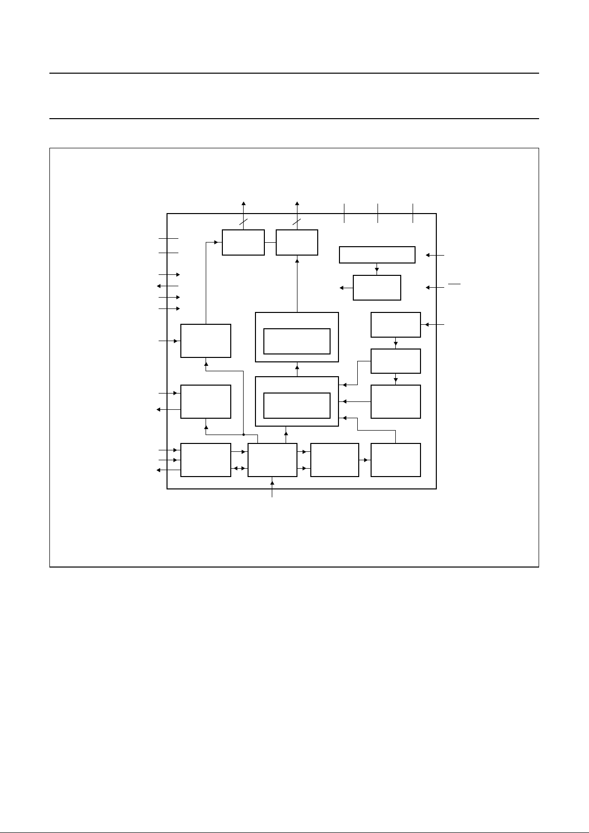
6 BLOCK DIAGRAM
handbook, full pagewidth
MGS465
DISPLAY DATA RAM
MATRIX DATA
RAM
DATA LATCHES
MATRIX
LATCHES
COLUMN
DRIVERS
C0 to C127
PCF8531
R0 to R33
ROW
DRIVERS
COMMAND
DECODER
ADDRESS
COUNTER
DISPLAY
ADDRESS
COUNTER
TIMING
GENERATOR
OSCILLATOR
INTERNAL
RESET
POWER-ON RESET ENR
RES
OSC
I2C-BUS
CONTROL
INPUT
FILTERS
SA0
SCL
SDA
SDACK
V
LCDOUT
V
LCDSENSE
V
LCDIN
T4
T3
T2
T1
34
V
SS2
V
SS1
V
DD1
V
DD2
V
DD3
V
LCD
GENERATOR
BIAS
VOLTAGE
GENERATOR
128
Fig.1 Block diagram.

2000 Feb 11 5
Philips Semiconductors Product specification
34 × 128 pixel matrix driver PCF8531
7 PINNING
SYMBOL PAD DESCRIPTION
1 to 14 dummy pads
OSC 15 oscillator input; note 1
V
LCDSENSE
16 voltage multiplier regulation input (V
LCD
); note 2
V
LCDOUT
17 to 23 voltage multiplier output (V
LCD
); note 3
V
LCDIN
24 to 30 LCD supply voltage (V
LCD
); note 2
RES 31 external reset input (active LOW); note 4
V
DD3
32 to 34 supply voltage 3; note 5
V
DD2
35 to 42 supply voltage 2; note 5
V
DD1
43 to 49 supply voltage 1; note 5
SDA 50 and 51 serial data line input of the I
2
C-bus
SDACK 52 serial data acknowledge output; note 6
53 dummy pad
SA0 54 I
2
C-bus slave address input; bit 0
ENR 55 enable internal Power-on reset input; note 7
T4 56 test 4 input; note 8
V
SS2
57 to 63 ground 2; note 9
V
SS1
64 to 70 ground 1; note 9
T3 71 test 3 input; note 8
T1 72 test 1 input; note 8
SCL 73 and 74 serial clock line input of the I
2
C-bus
75 to 77 dummy pads
T2 78 test 2 output; note 10
79 to 86 dummy pads
R0 87 LCD row driver output
R2 88 LCD row driver output
R4 89 LCD row driver output
R6 90 LCD row driver output
R8 91 LCD row driver output
R10 92 LCD row driver output
R12 93 LCD row driver output
R14 94 LCD row driver output
R16 95 LCD row driver output
R18 96 LCD row driver output
R20 97 LCD row driver output
R22 98 LCD row driver output
R24 99 LCD row driver output
R26 100 LCD row driver output
R28 101 LCD row driver output
R30 102 LCD row driver output
R32 103 LCD row driver output
2000 Feb 11 6
Philips Semiconductors Product specification
34 × 128 pixel matrix driver PCF8531
Notes
1. If the on-chip oscillator is used, this input must be connected to V
DD1
.
2. If the internal V
LCD
generation is used, V
LCDOUT
, V
LCDIN
and V
LCDSENSE
must be connected together.
3. If an external V
LCD
is used in the application, then pin V
LCDOUT
must be left open circuit, otherwise the chip will be
damaged.
4. If only the internal Power-on reset is used, this input must be connected to V
DD1
.
5. V
DD1
is for the logic supply, V
DD2
, and V
DD3
are for the voltage multiplier. For split power supplies, V
DD2
and V
DD3
must be connected together. If only one supply voltage is available, V
DD1,VDD2
and V
DD3
must be connected
together.
6. Serial data acknowledge for the I2C-bus. By connecting SDACK to SDA externally, the SDA line becomes fully
I2C-bus compatible. Having the acknowledge output separated from the serial data line is advantageous in
Chip-On-Glass (COG) applications. In COG applications where the track resistance from the SDACK pad to the
system SDA line can be significant, a potential divider is generated by the bus pull-up resistor and the Indium Tin
Oxide (ITO) track resistance. It is possible that the PCF8531 will not be able to create a valid logic 0 level during the
acknowledge cycle. By splitting the SDA input from the SDACK output, the device could be used in a mode that
ignores the acknowledge bit. In COG applications where the acknowledge cycle is required, it is necessary to
minimize the track resistance from the SDACK pad to the system SDA line to guarantee a valid LOW level.
7. If ENR is connected to VSS, Power-on reset is disabled; to enable Power-on reset ENR should be connected to V
DD1
.
8. In the application, this input must be connected to VSS.
9. V
SS1
and V
SS2
must be connected together.
10. In the application, T2 must be left open circuit.
C0 to C127 104 to 231 LCD column driver outputs
R33 232 LCD row driver output; icon row
R31 233 LCD row driver output
R29 234 LCD row driver output
R27 235 LCD row driver output
R25 236 LCD row driver output
R23 237 LCD row driver output
R21 238 LCD row driver output
R19 239 LCD row driver output
R17 240 LCD row driver output
R15 241 LCD row driver output
R13 242 LCD row driver output
R11 243 LCD row driver output
R9 244 LCD row driver output
R7 245 LCD row driver output
R5 246 LCD row driver output
R3 247 LCD row driver output
R1 248 LCD row driver output
SYMBOL PAD DESCRIPTION

2000 Feb 11 7
Philips Semiconductors Product specification
34 × 128 pixel matrix driver PCF8531
8 FUNCTIONAL DESCRIPTION
8.1 Oscillator
The on-chip oscillator provides the clock signal for the
display system. No external components are required and
the OSC input must be connected to VDD. An external
clock signal, if used, is connected to this input.
8.2 Power-on reset
The on-chip Power-on reset initializes the chip after
Power-on or power failure.
8.3 I
2
C-bus controller
The I2C-bus controller receives and executes the
commands. The PCF8531 acts as an I2C-bus slave
receiver and therefore cannot control bus communication.
8.4 Input filters
To enhance noise immunity in electrically adverse
environments, RC low-pass filters are provided on the
SDA and SCL lines.
8.5 Display data RAM
The PCF8531 contains a 34 × 128 bits static RAM, which
storesthe display data.The RAM is dividedinto 6 banks of
128 bytes (6 × 8 × 128 bits). Bank 6 is used for icon data.
DuringRAM access, datais transferred tothe RAM viathe
I2C-bus interface. There is a direct correspondence
between the X address and column output number.
8.6 Timing generator
The timing generator produces the various signals
required to drive the internal circuitry. Internal chip
operation is notdisturbed by operations on the data buses.
8.7 Address counter
The address counter sets the addresses of the display
data RAM for writing.
8.8 Display address counter
The display address counter generates the addresses for
read out of the display data.
8.9 Command decoder
The command decoder identifies command words that
arrive on the I2C-bus and determines the destination for
the following data bytes.
8.10 Bias voltage generator
The bias voltage generator generates four buffered
intermediate bias voltages. This block contains the
generator for the reference voltages and the four buffers.
This block can operate in two voltage ranges:
• Normal mode; 4.0 to 9.0 V
• Power save mode; 3.0 to 9.0 V.
8.11 V
LCD
generator
The V
LCD
voltage generator contains a configurable
2 to 5 times voltage multiplier; this is software
programmable.
8.12 Reset
The PCF8531 has the possibility of two reset modes,
internal Power-on reset or external reset (
RES). The reset
mode is selected using the ENR signal. After a reset, the
chip has the following state:
• All row and column outputs are set to VSS (display off)
• RAM data is undefined
• Power-down mode.
8.13 Power-down
During power-down, allstatic currents are switched off (no
internal oscillator, no timing and no LCD segment drive
system), and all LCD outputs are internally connected to
VSS. The I2C-bus function remains operational.
8.14 Column driver outputs
The LCD drive section includes 128 column outputs
(C0 to C127) which should be connected directly to the
LCD. The column output signals are generated in
accordance with the multiplexed row signals and with the
data in the display latch. When less than 128 columns are
required, the unused column outputs should be left open
circuit.
8.15 Row driver outputs
The LCD drive section includes 34 row outputs
(R0 to R33), which should be connected directly to the
LCD. The row output signals aregenerated in accordance
with the selected LCD drive mode. If less than 34 rows or
lower Mux rates are required, the unused outputs must be
left open circuit. The row signals are interlaced i.e. the
selection order is R0, R2, ..., R1, R3 etc.
2000 Feb 11 8
Philips Semiconductors Product specification
34 × 128 pixel matrix driver PCF8531
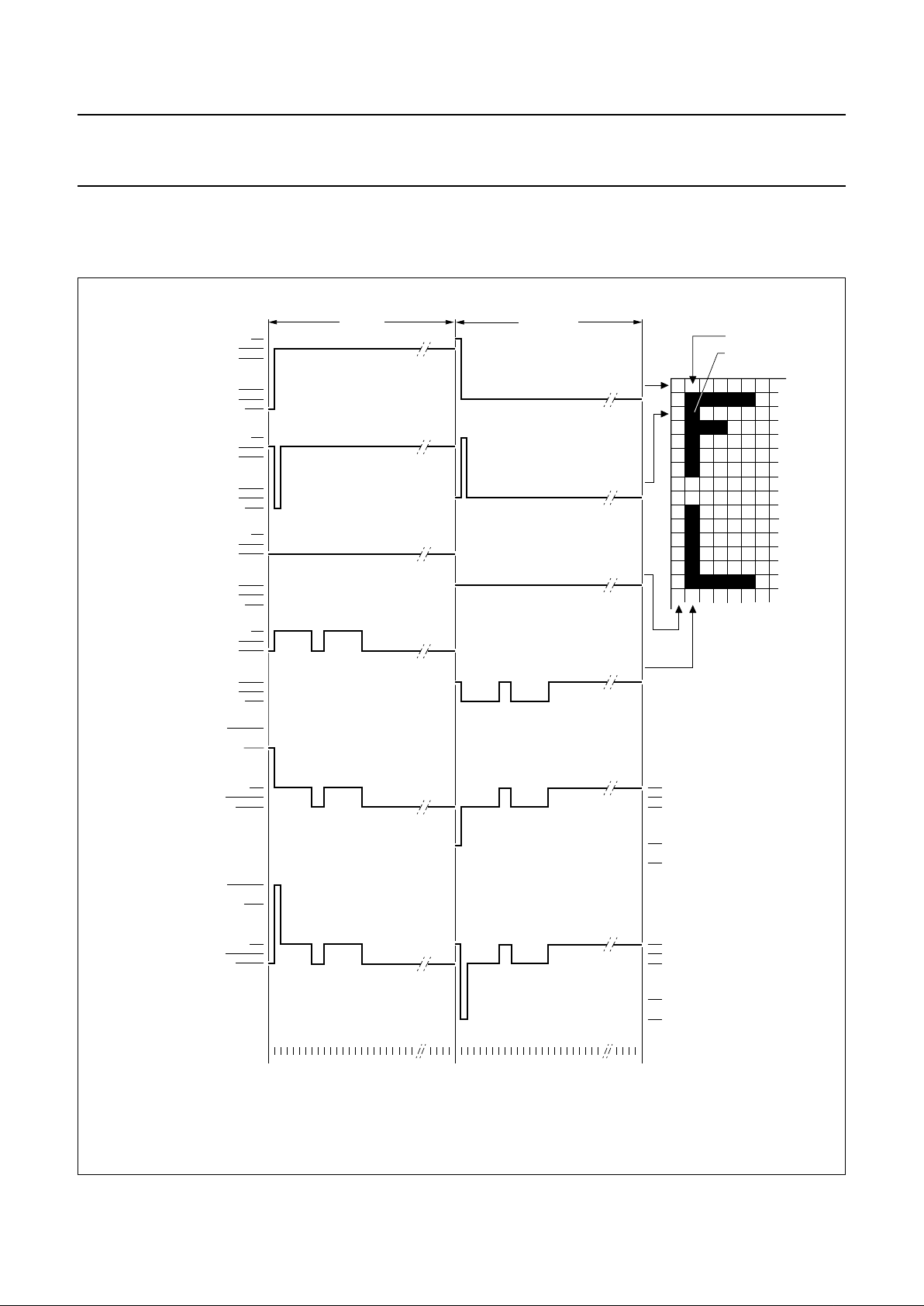
8.16 LCD waveforms and DDRAM to data mapping
The LCD waveforms and the DDRAM to display data mapping are shown in Figs 2, 3 and 4.
MGS466
ROW 0
R0 (t)
ROW 2
R2 (t)
COL 0
C0 (t)
COL 1
C1 (t)
0 V
0 V
V3 − V
SS
frame n frame n + 1
02468... 1 35 7... ... 33... 32 02468... 1 3 5 7... ... 33... 32
V
state1
(t)
V
state1
(t)
V
state2
(t)
V
LCD
V
2
V
3
V
4
V
5
V
SS
V
LCD
V
2
V
3
V
4
V
5
V
SS
V
LCD
V
2
V
3
V
4
V
5
V
SS
V
LCD
V
2
V
3
V
4
V
5
V
SS
V
LCD
V
LCD
− V
2
V4 − V
5
VSS − V
5
V4 − V
LCD
V3 − V
2
−V
LCD
0 V
0 V
V3 − V
SS
V
state2
(t)
V
LCD
V
LCD
− V
2
V4 − V
5
V4 − V
LCD
V3 − V
2
VSS − V
5
−V
LCD
Fig.2 Typical LCD driver waveforms.
V
state1
(t) = C1(t) − R0(t).
V
state2
(t) = C1(t) − R2(t).
2000 Feb 11 9
Philips Semiconductors Product specification
34 × 128 pixel matrix driver PCF8531
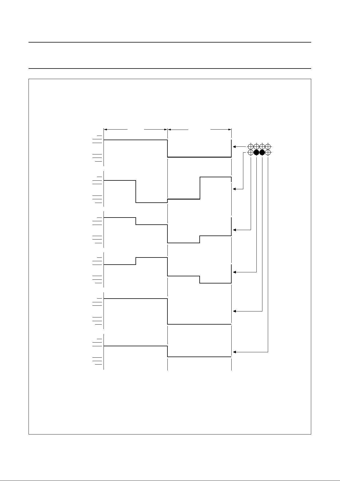
MGS467
ROW 0 to 32
ROW 33
COL 1 on/off
COL 2 off/on
COL 3 on/on
COL 4 off/off
frame n frame n + 1
V
LCD
V
2
V
3
V
4
V
5
V
SS
V
LCD
V
2
V
3
V
4
V
5
V
SS
V
LCD
V
2
V
3
V
4
V
5
V
SS
V
LCD
V
2
V
3
V
4
V
5
V
SS
V
LCD
V
2
V
3
V
4
V
5
V
SS
V
LCD
V
2
V
3
V
4
V
5
V
SS
only icons are driven
Fig.3 Icon mode; Mux 1 : 2 LCD waveforms.
2000 Feb 11 10
Philips Semiconductors Product specification
34 × 128 pixel matrix driver PCF8531
top of LCD
MGS468
bank 0
bank 1
bank 2
bank 3
bank 4
R32
R24
R16
R8
R0
R33 (icon row)
bank 5
LCD
DDRAM
Fig.4 DDRAM to display mapping.
2000 Feb 11 11
Philips Semiconductors Product specification
34 × 128 pixel matrix driver PCF8531
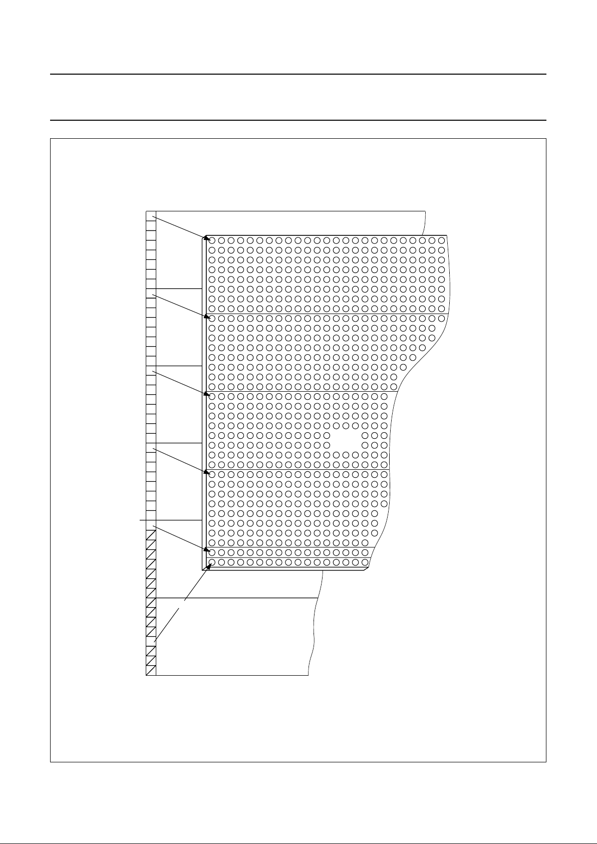
8.17 Addressing
Data is written in bytes into the RAM matrix of the
PCF8531 as illustrated in Figs 5, 6 and 7. The display
RAM has a matrix of 34 × 128 bits. The columns are
addressedbytheaddress pointer. The address rangesare
X 0 to X 127 (7FH) and Y 0 to Y 5 (5H). Addresses
outside of these ranges are not allowed. In vertical
addressing mode (V = 1), the Y address increments after
each byte (see Fig.6). After the last Y address (Y = 4),
Y wraps around to 0 and X increments to address thenext
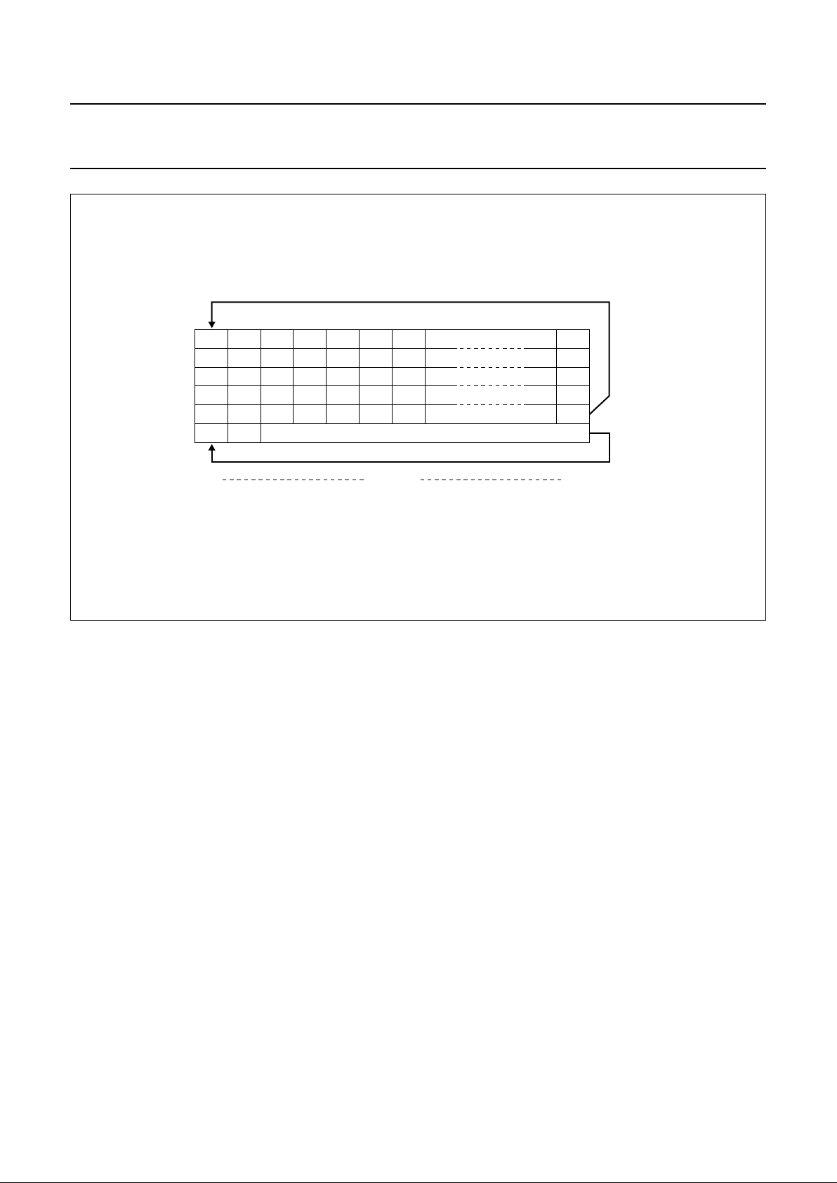
column. In horizontal addressing mode (V = 0), the
X addressincrements after each byte (seeFig.7).After the
last X address (X = 127), X wraps around to 0 and
Y increments to address the next row. After the very last
address (X = 127 and Y = 4), the address pointers wrap
around to address (X = 0 and Y = 0). It should be noted
thatin bank 4 onlythe LSB (DB0)of the data willbe written
into the RAM. The Y address 5 is reserved for icon data
and is not affected by the addressing mode; it should be
noted that in bank 5 only the 5th data bit (DB4) will be
written into the RAM.
handbook, full pagewidth
MGS469
0
1
2
3
5
4
0 127X address
icon data
Y address
LSB
MSB
LSB
MSB
LSB
MSB
Fig.5 RAM format and addressing.
handbook, full pagewidth
MGS470
05
16
2
3
4
0 1 icon data
0
1
2
3
4
5
638
639
0 127X address
Y address
Fig.6 Sequence of writing data bytes into RAM with vertical addressing (V = 1).
2000 Feb 11 12
Philips Semiconductors Product specification
34 × 128 pixel matrix driver PCF8531
handbook, full pagewidth
MGS471
012
128 129 130
256 257 258
384 385 386
512 513 514
0 1 icon data
0
1
2
3
4
5
127
255
383
511
639
0 127X address
Y address
Fig.7 Sequence of writing data bytes into RAM with horizontal addressing (V = 0).
8.18 Instructions
Only two PCF8531 registers, the Instruction Register (IR)
and the Data Register (DR) can be directly controlled by
the MPU. Before internal operation, control information is
stored temporarily in these registers to allow interfacing to
various types of MPUs which operate at different speeds
or to allow interfacing to peripheral control ICs.
The PCF8531 operation is controlled by the instructions
given in Table 1. Details are explained in subsequent
sections.
Instructions are of four types:
1. Those that define PCF8531 functions such as display
configuration, etc.
2. Those that set internal RAM addresses
3. Those that perform data transfer with internal RAM
4. Others.
In normal use, category 3 instructions are used most
frequently. Automatic incrementing by 1 of internal RAM
addressesafter each data write reducestheMPU program
load.
8.18.1 RESET
After reset or internal Power-on reset (depending on
application), the LCD driver will be set to the following
state:
• Power-down mode (PD = 1)
• Horizontal addressing (V = 0)
• Display blank (D = 0; E = 0), no icon mode (IM = 0)
• Address counter X[6:0] = 0; Y[2:0] = 0
• Bias system BS[2:0] = 0
• Multiplex rate M[1:0] = 0 (Mux rate 1 : 17)
• Temperature control mode TC[2:0] = 0
• HV-gen control, HVE = 0 the HV generator is switched
off, PRS = 0 and S[1:0] = 0
• V
LCD
=0V
• RAM data is undefined
• Command page definition H[1:0] = 0.
2000 Feb 11 13
Philips Semiconductors Product specification
34 × 128 pixel matrix driver PCF8531
8.18.2 FUNCTION SET
8.18.2.1 PD
When PD = 1, the Power-down mode of the LCD driver is
active:
• All LCD outputs at VSS (display off)
• Power-on reset detection active, oscillator off
• V
LCD
can be disconnected
• I2C-bus is operational, commands can be executed
• RAM contents not cleared; RAM data can be written
• Register settings remain unchanged.
8.18.2.2 V
When V = 0 the horizontal addressing is selected.
The data is written into the DDRAM as shown in Fig.7.
When V = 1 the vertical addressing is selected. The data
is written into the DDRAM as shown in Fig.6. Icon data is
written independently of V when Y address is 5.
8.18.3 SET Y ADDRESS
Bits Y2,Y1and Y0 define the Y address vector of the
display RAM.
Table 1 Yaddress
8.18.4 SET X ADDRESS
The X address points to the columns. The range of X is
0 to 127 (7FH).
8.18.5 SET MULTIPLEX RATE
M[1:0] selects the multiplex rate (see Table 8).
8.18.6 DISPLAY CONTROL (D, E AND IM)
Bits D and E select the display mode (see Table 6). Bit IM
sets the display to icon mode.
8.18.7 SET BIAS SYSTEM
Different multiplex rates require different bias settings.
These are programmed by BS[2:0], which sets the binary
number n. The optimum value for n is given by
Supported values of n are given in Table 2. Table 3shows
the intermediate bias voltages.
Y
2
Y
1
Y
0
BANK
0000
0011
0102
0113
1004
1 0 1 5 (icons)
n Mux rate 3–=
Table 2 Programming the required bias system
BS[2] BS[1] BS[0] n BIAS SYSTEM COMMENT
0007
1
⁄
11
0016
1
⁄
10
0105
1
⁄
9
0114
1
⁄
8
1003
1
⁄
7
recommended for 1 : 34
1012
1
⁄
6
recommended for 1 : 26
1101
1
⁄
5
recommended for 1 : 17
1110
1
⁄
4
recommended for icon mode
2000 Feb 11 14
Philips Semiconductors Product specification
34 × 128 pixel matrix driver PCF8531
8.18.8 LCD BIAS VOLTAGE
Table 3 Intermediate LCD bias voltages
8.18.9 S
ET VOPVALUE:
The operating voltage V
LCD
can be set by software.
The voltageat reference temperature[V
LCD
(T = T
cut
)]can
be calculated as: V
LCD
(T
cut
)=(a+VOP× b).
The generated voltage is dependent on the temperature,
programmed Temperature Coefficient (TC) and the
programmed voltage at reference temperature (T
cut
).
V
LCD=VLCD
(T
cut
) × [1+TC×(T − T
cut
)].
The parameter values are given in Table 4.
Two overlapping V
LCD
ranges can be selected via the
command ‘HV-gen control’ (see Table 4 and Fig.8).
The maximum voltage that can be generated depends on
the V
DD2
and V
DD3
voltages and the display load current.
For Mux 1 : 34,the optimum operatingvoltage of theliquid
can be calculated as:
Where V
th
is the threshold voltage of the liquid crystal
material used.
The practical value for VOP is determined by equating
V
off(rms)
with a defined LCD threshold voltage (Vth),
typically when the LCD exhibits approximately
10% contrast.
As the programming range for the internally generated
V
LCD
allows values abovethe maximum allowed V
LCD
, the
user has to ensure, while setting the VOP register and
selecting the temperature compensation, that the V
LCD
limit of maximum 9 V will never be exceeded under all
conditions and including all tolerances.
SYMBOL
BIAS
VOLTAGES
EXAMPLE FOR
1
⁄7BIAS
V1 V
LCD
V
LCD
V2
6
⁄7× V
LCD
V3
5
⁄7× V
LCD
V4
2
⁄7× V
LCD
V5
1
⁄7× V
LCD
V6 V
SS
V
SS
n3+
n4+
------------ -
V
LCD
×
n2+
n4+
------------ -
V
LCD
×
2
n4+
------------ -
V
LCD
×
1
n4+
------------ -
V
LCD
×
V
LCD
134+
21
1
34
----------
–
×
---------------------------------------
V
th
× 5.30 Vth×==
Table 4 Parameter values for the HV generator programming
SYMBOL
VALUE
UNIT
PRS=0 PRS=1
T
cut
27 27 °C
a 2.94 6.75 V
b 0.03 0.03 V
Programming range 2.94 to 6.75 6.75 to 10.56 V
 Loading...