

Philips PCD3350A Datasheet

INTEGRATED CIRCUITS
DATA SH EET
PCD3350A
8-bit microcontroller with DTMF
generator, 256 bytes EEPROM and
real-time clock
Product specification
Supersedes data of 1996 May 09
File under Integrated Circuits, IC03
1996 Dec 18

Philips Semiconductors Product specification
8-bit microcontroller with DTMF generator,
256 bytes EEPROM and real-time clock
CONTENTS
1 FEATURES
2 GENERAL DESCRIPTION
3 ORDERING INFORMATION
4 BLOCK DIAGRAM
5 PINNING INFORMATION
5.1 Pinning
5.2 Pin description
6 FREQUENCY GENERATOR
6.1 Frequency generator derivative registers
6.2 Melody output (P1.7/MDY)
6.3 DTMF clock divider and output (DP1.7/DCO)
6.4 Frequency registers
6.5 DTMF frequencies
6.6 Modem frequencies
6.7 Musical scale frequencies
7 EEPROM AND TIMER 2 ORGANIZATION
7.1 EEPROM registers
7.2 EEPROM latches
7.3 EEPROM flags
7.4 EEPROM macros
7.5 EEPROM access
7.6 Timer 2
8 REAL-TIME CLOCK
8.1 Oscillator
8.2 Divider chain
8.3 Frequency adjustment
8.4 Real-time clock derivative registers
9 DERIVATIVE INTERRUPTS
10 TIMING
11 RESET
12 IDLE MODE
13 STOP MODE
14 SUMMARY OF I/O PORTS AND ROM MASK
15 SUMMARY OF DERIVATIVE REGISTERS
16 HANDLING
17 LIMITING VALUES
18 DC CHARACTERISTICS
19 AC CHARACTERISTICS
20 PACKAGE OUTLINES
21 SOLDERING
21.1 Introduction
21.2 Reflow soldering
21.3 Wave soldering
21.4 Repairing soldered joints
22 DEFINITIONS
23 LIFE SUPPORT APPLICATIONS
PCD3350A
OPTIONS
1996 Dec 18 2

Philips Semiconductors Product specification
8-bit microcontroller with DTMF generator,
256 bytes EEPROM and real-time clock
1 FEATURES
• 8-bit CPU, ROM, RAM, EEPROM, real-time clock and
I/O; all in a 44-lead quad flat package
• 8 kbytes ROM
• 256 bytes RAM
• 256 bytes Electrically Erasable Programmable Read
Only Memory (EEPROM)
• 32 kHz crystal oscillator for Real-Time Clock (RTC)
• EEPROM programmable RTC
• Over 100 instructions (based on MAB8048) all of
1 or 2 cycles
• 34 quasi-bidirectional I/O port lines
• 8-bit programmable Timer/event counter 1
• 8-bit reloadable Timer 2
• Three single-level vectored interrupts:
– external
– 8-bit programmable Timer/event counter 1
– derivative; triggered by reloadable Timer 2
• Two test inputs, one of which also serves as the external
interrupt input
• DTMF, modem, musical tone generator
• Reference for supply and temperature-independent
tone output
• Filtering for low output distortion (CEPT compatible)
• Melody output for ringer application
• Programmable DTMF clock divider
• Power-on-reset
• Stop and Idle modes
PCD3350A
• Supply voltage: 1.8 to 6 V (DTMF tone output and
EEPROM erase/write from 2.5 V)
• CPU clock frequency: 1 to 16 MHz (3.58 MHz or
10.74 MHz for DTMF)
• Operating ambient temperature: −25 to +70 °C
• Manufactured in silicon gate CMOS process.
2 GENERAL DESCRIPTION
This data sheet details the specific properties of the
PCD3350A. The shared properties of the PCD33xxA
family of microcontrollers are described in the
data sheet, which should be read in conjunction
family”
with this publication.
The PCD3350A is a microcontroller designed primarily for
telephony applications. It includes 8 kbytes ROM,
256 bytes RAM, 34 I/O lines, and an on-chip generator for
dual tone multifrequency (DTMF), modem and musical
tones. In addition to dialling, the generated frequencies
can be made available as square waves for melody
generation, providing ringer operation.
The PCD3350A also incorporates 256 bytes of EEPROM,
permitting data storage without battery backup. The
EEPROM can be used for storing telephone numbers,
particularly for implementing redial functions.
Finally, the PCD3350A includes a low power 32 kHz
crystal oscillator with an EEPROM programmable
Real-Time Clock (RTC) working in standby mode.
The instruction set is similar to that of the MAB8048 and is
a sub-set of that listed in the
sheet.
“PCD33xxA family”
“PCD33xxA
data
3 ORDERING INFORMATION (see note 1)
TYPE NUMBER
NAME DESCRIPTION VERSION
PCD3350AH QFP44 plastic quad flat package; 44 leads (lead length 2.35 mm);
body 14 × 14 × 2.2 mm
Note
1. Please refer to the Order Entry Form (OEF) for this device for the full type number to use when ordering. This type
number will also specify the required program and the ROM mask options.
1996 Dec 18 3
PACKAGE
SOT205-1
Philips Semiconductors Product specification
8-bit microcontroller with DTMF generator,
256 bytes EEPROM and real-time clock
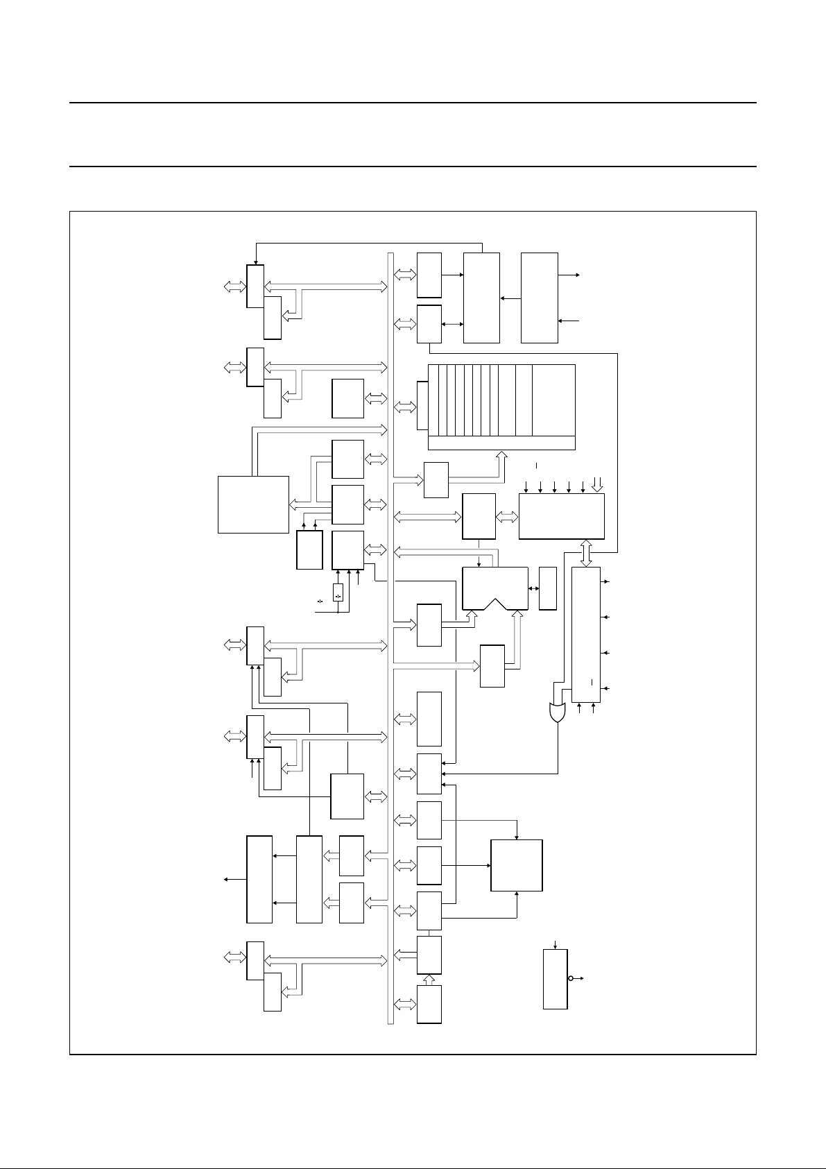
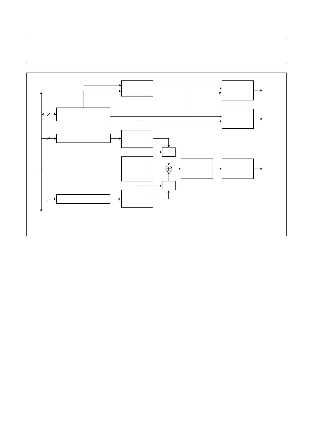
4 BLOCK DIAGRAM
WORD
STATUS
PROGRAM
LOWER
COUNTER
PROGRAM
HIGHER
COUNTER
PROGRAM
EVENT
TIMER/
COUNTER
32
T1
CONTROL
REGISTER
& MELODY
DTMF-CLOCK
LGF
REGISTER
HGF
REGISTER
6
8 8
8
58888
8
8
88
8
8
8
8
8
8
8
8
8
8
8
8
8
4
8
6
BUFFER
DER. PORT 0
DP0.0/RCO to DP0.5
8
PORT 0
BUFFER
P0.0 to P0.7
ROM
8 kbytes
RESIDENT
PCD3350A
PORT 1
BUFFER
P1.0 to P1.7/MDY
8
BUFFER
DER. PORT 1
DP1.0 to DP1.7/DCO
DTMF
f
TONE
FILTER
4 8
PORT 2
BUFFER
P2.0 to P2.3
FLIP-FLOP
DER. PORT 0
PORT 0
FLIP-FLOP
DECODE
PORT 1
FLIP-FLOP
FLIP-FLOP
DER. PORT 1
PORT 2
FLIP-FLOP
BANK
MEMORY
FLIP-FLOPS
FREQ.
CLOCK
INTERNAL
SINE WAVE
GENERATOR
30
REGISTER
FREQUENCY
ADJUSTMENT
CLOCK
CONTROL
REGISTER
REGISTER 0
REGISTER 1
REGISTER 2
MULTIPLEXER
RAM
ADDRESS
REGISTER
REGISTER 1
TEMPORARY
timer interrupt
ACCUMULATOR
LOGIC
INTERRUPT
DATA
EEPROM
TRANSFER
EEPROM
ADDRESS
REGISTER
EEPROM
CONTROL
REGISTER
TIMER 2
REGISTER
TIMER 2
RELOAD
REGISTER
REAL-TIME CLOCK
REGISTER 3
REGISTER 4
REGISTER 5
AND
REGISTER
INSTRUCTION
ARITHMETIC
interrupt
derivative
DIVIDER CHAIN
REGISTER 6
REGISTER 7
8 LEVEL STACK
(VARIABLE LENGTH)
DECOD
DECODER
LOGIC UNIT
REGISTER 2
TEMPORARY
EEPROM
REAL-TIME CLOCK
32 kHz OSCILLATOR
RTC1 RTC2
DATA STORE
REGISTER BANK
OPTIONAL SECOND
E
FLAG
T1
CE/T0
TIMER
BRANCH
CONDITIONAL
ADJUST
DECIMAL
RTC interrupt
external interrupt
256 bytes
POR
V
POWER-ON-RESET
256 bytes
RESIDENT RAM ARRAY
TEST
ACC BIT
ACC
CARRY
LOGIC
XTAL2XTAL1RESET
CONTROL AND TIMING
CE/T0
IDLE
STOP
RESET
PCD3350A
MED263
OSCILLATOR
handbook, full pagewidth
Fig.1 Block diagram.
INTERRUPT INITIALIZE
1996 Dec 18 4
Philips Semiconductors Product specification
8-bit microcontroller with DTMF generator,
256 bytes EEPROM and real-time clock
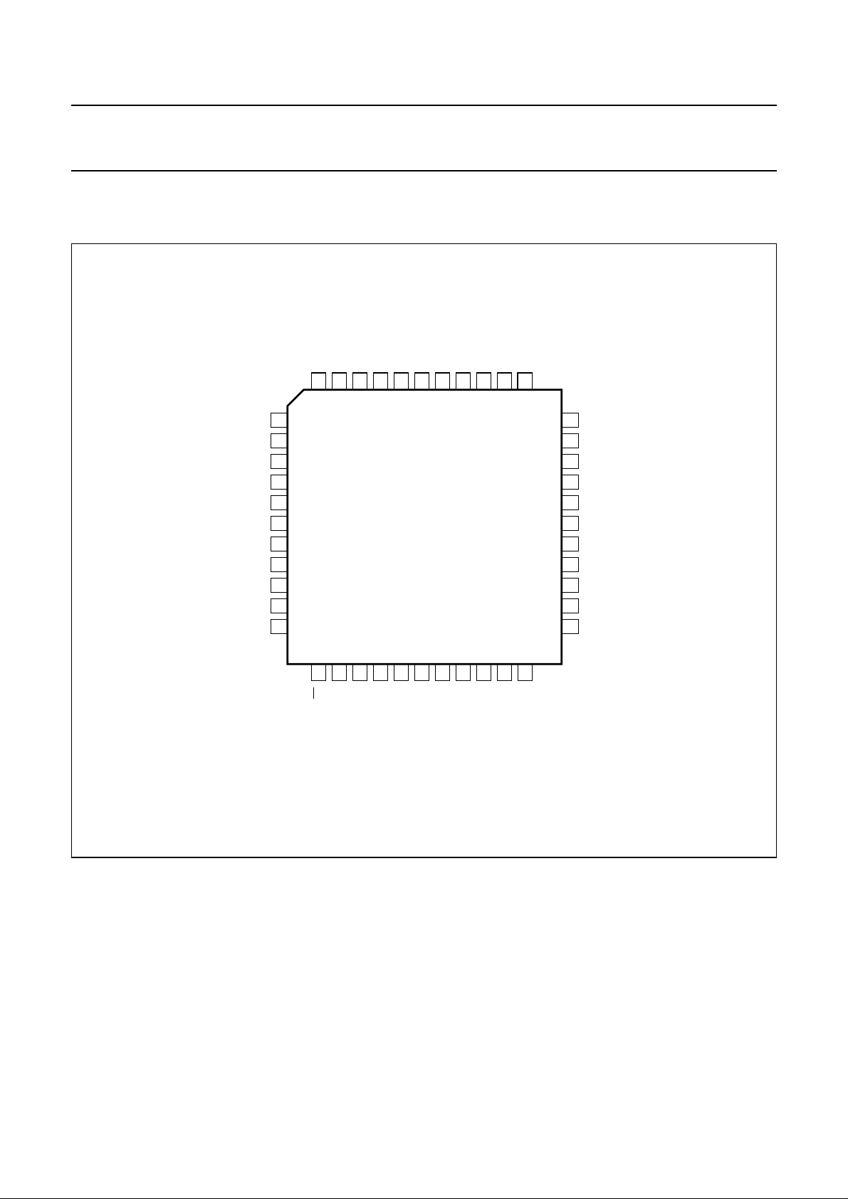
5 PINNING INFORMATION
5.1 Pinning
handbook, full pagewidth
P1.6
P1.7/MDY
43
42
P1.5
P1.4
41
40
PCD3350AH
P2.1
P2.2
P2.3
DP0.0/RCO
DP0.1
DP0.2
DP0.3
DP0.4
DP0.5
RTC1
RTC2
P2.0
44
1
2
3
4
5
6
7
8
9
10
11
P1.3
39
PCD3350A
SS
DD
TONE
V
38
37
P1.1
V
P1.2
36
35
34
33
P1.0
P0.7
32
31
P0.6
30
P0.5
P0.4
29
28
XTAL2
XTAL1
27
P0.3
26
P0.2
25
24
P0.1
P0.0
23
12
13
14
15
16
T1
CE/T0
DP1.0
RESET
DP1.1
Fig.2 Pin configuration.
17
DP1.2
18
DP1.3
19
DP1.4
20
DP1.5
21
DP1.6
22
MED264
DP1.7/DCO
1996 Dec 18 5
Philips Semiconductors Product specification
8-bit microcontroller with DTMF generator,
PCD3350A
256 bytes EEPROM and real-time clock
5.2 Pin description
Table 1 SOT205-1 package (for information on parallel I/O ports, see Chapter 14)
SYMBOL PIN TYPE DESCRIPTION
P2.1 to P2.3 1 to 3 I/O 3 bits of Port 2: 4-bit quasi-bidirectional I/O port
DP0.0/RCO 4 I/O 1 bit of Derivative Port 0: 6-bit quasi-bidirectional I/O port; or RTC output
DP0.1 to DP0.5 5 to 9 I/O 5 bits of Derivative Port 0: 6-bit quasi-bidirectional I/O port
RTC1 10 I Real Time Clock 32 kHz oscillator input
RTC2 11 O Real Time Clock 32 kHz oscillator output
CE/
T0 12 I Chip Enable or Test 0 input
T1 13 I Test 1/count input of 8-bit Timer/event counter 1
RESET 14 I reset input
DP1.0 to DP1.6 15 to 21 I/O 7 bits of Derivative Port 1: 8-bit quasi-bidirectional I/O port
DP1.7/DCO 22 I/O 1 bit of Derivative Port 1: 8-bit quasi-bidirectional I/O port; or DTMF clock
output
P0.0 to P0.3 23 to 26 I/O 4 bits of Port 0: 8-bit quasi-bidirectional I/O port
XTAL1 27 I crystal oscillator/external clock input
XTAL2 28 O crystal oscillator output
P0.4 to P0.7 29 to 32 I/O 4 bits of Port 0: 8-bit quasi-bidirectional I/O port
P1.0 to P1.2 33 to 35 I/O 3 bits of Port 1: 8-bit quasi-bidirectional I/O port
V
SS
TONE 37 O DTMF output
V
DD
P1.3 to P1.6 39 to 42 I/O 4 bits of Port 1: 8-bit quasi-bidirectional I/O port
P1.7/MDY 43 I/O 1 bit of Port 1: 8-bit quasi-bidirectional I/O port; or melody output
P2.0 44 I/O 1 bit of Port 2: 4-bit quasi-bidirectional I/O port
36 P ground
38 P positive supply voltage
1996 Dec 18 6
Philips Semiconductors Product specification
8-bit microcontroller with DTMF generator,
PCD3350A
256 bytes EEPROM and real-time clock
6 FREQUENCY GENERATOR
A versatile frequency generator section with built-in
programmable clock divider is provided (see Fig.3).
The clock divider allows the DTMF section to run either
with the main clock frequency (f
of it (f
DTMF
=1⁄3× f
) depending on the state of the divider
xtal
DTMF=fxtal
) or with a third
control bit DIV3 (see Table 4). The frequency generator
includes precision circuitry for dual tone multifrequency
(DTMF) signals, which is typically used for tone dialling
telephone sets.
6.1 Frequency generator derivative registers
6.1.1 H
IGH AND LOW GROUP FREQUENCY REGISTERS
Table 2 gives the addresses, symbols and access types of the High Group Frequency (HGF) and Low Group Frequency
(LGF) registers, used to set the frequency output.
Table 2 Hexadecimal addresses, symbols, access types and bit symbols of the frequency registers
REGISTER
ADDRESS
REGISTER
SYMBOL
ACCESS
TYPE
7 6 5 4 3 2 1 0
11H HGF W H7H6H5H4H3H2H1H0
12H LGF W L7L6L5L4L3L2L1L0
The TONE output can alternatively issue twelve modem
frequencies for data rates between 300 and 1200 bits/s.
In addition to DTMF and modem frequencies, two octaves
of musical scale in steps of semitones are available. Their
frequencies are provided either in purely sinusoidal form
on the TONE output or as a square wave on the port line
P1.7/MDY. The latter is typically for ringer applications in
telephone sets. If no frequency output is selected the
TONE output is in 3-state mode.
BIT SYMBOLS
6.1.2 CLOCK AND MELODY CONTROL REGISTER (MDYCON)
Table 3 Clock and Melody Control Register, MDYCON (address 13H; access type R/W)
7 6 5 4 3 2 1 0
00000EDCO DIV3 EMO
Table 4 Description of MDYCON bits
BIT SYMBOL DESCRIPTION
7to3 − These bits are set to a logic 0.
2 EDCO Enable DTMF clock output. If bit EDCO = 0, then DP1.7/DCO is a general purpose
derivative port line. If bit EDCO = 1, then DP1.7/DCO is the DTMF clock output.
EDCO = 1 does not inhibit the port instructions for DP1.7/DCO. Therefore the state of
both port line and flip-flop may be read in and the port flip-flop may be written by
derivative port instructions. However, the port flip-flop of DP1.7/DCO must remain set to
avoid conflicts between DTMF clock and port outputs.
1 DIV3 Enable DTMF clock divider. If bit DIV3 = 0, then the DTMF clock f
If bit DIV3 = 1, then f
DTMF
=1⁄3× f
xtal
.
DTMF=fxtal
.
0 EMO Enable Melody Output. If bit EMO = 0, then P1.7/MDY is a standard port line.
If bit EMO = 1, then P1.7/MDY is the melody output. EMO = 1 does not inhibit the port
instructions for P1.7/MDY. Therefore the state of both port line and flip-flop may be read
in and the port flip-flop may be written by port instructions. However, the port flip-flop of
P1.7/MDY must remain set to avoid conflicts between melody and port outputs.
When the HGF contents are zero while EMO = 1, P1.7/MDY is in the HIGH state.
1996 Dec 18 7
Philips Semiconductors Product specification
8-bit microcontroller with DTMF generator,
256 bytes EEPROM and real-time clock
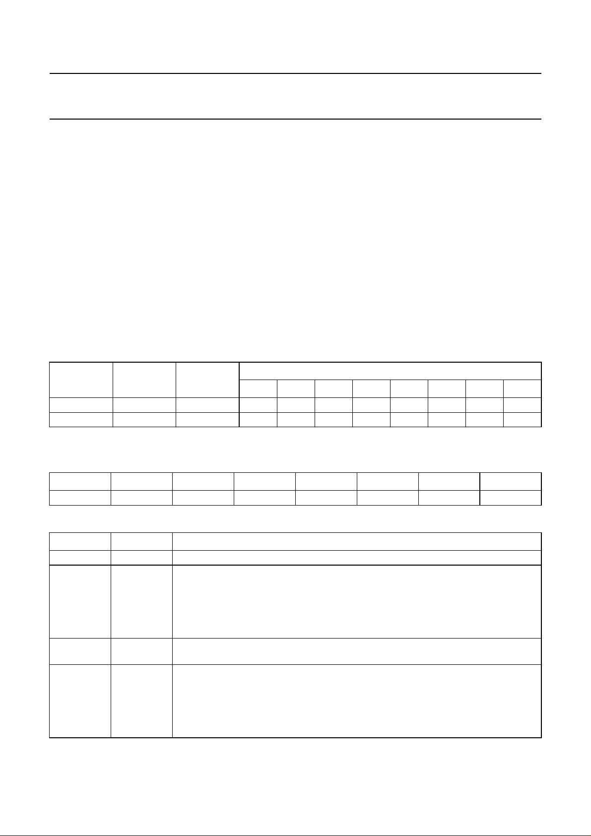
handbook, full pagewidth
8
8
8
INTERNAL BUS
8
f
xtal
CLOCK AND MELODY
CONTROL REGISTER
HGF REGISTER
LGF REGISTER
CLOCK
DIVIDER
DIGITAL
SINE WAVE
SYNTHESIZER
SWITCHED
CAPACITOR
BANDGAP
VOLTAGE
REFERENCE
DIGITAL
SINE WAVE
SYNTHESIZER
f
square wave
DAC
DAC
DTMF
SWITCHED
CAPACITOR
LOW-PASS
FILTER
PCD3350A
PORT/CLOCK
OUTPUT LOGIC
PORT/MELODY
OUTPUT LOGIC
RC LOW-PASS
FILTER
MGB782
DP1.7/
DCO
P1.7/
MDY
TONE
Fig.3 Block diagram of the frequency generator, melody output (P1.7/MDY) and DTMF clock output
(DP1.7/DCO).
6.2 Melody output (P1.7/MDY)
The melody output (P1.7/MDY) is very useful for
generating musical notes when a purely sinusoidal signal
is not required, such as for ringer applications.
The square wave (duty cycle =12⁄23 or 52%) will include
the attenuated harmonics of the base frequency, which is
defined by the contents of the HGF register (Table 2).
However, even higher frequency notes may be produced
since the low-pass filtering on the TONE output is not
applied to the P1.7/MDY output. This results in the
minimum decimal value x in the HGF register (see
equation in Section 6.4) being 2 for the P1.7/MDY output,
rather than 60 for the TONE output. A sinusoidal TONE
output is produced at the same time as the melody square
wave, but due to the filtering, the higher frequency sine
waves produced when x < 60 will not appear at the TONE
output.
Since the melody output is shared with P1.7, the port
flip-flop of P1.7 has to be set HIGH before using the
6.3 DTMF clock divider and output (DP1.7/DCO)
The DTMF clock divider allows the DTMF part to run either
with the main clock frequency (f
of it (f
DTMF
=1⁄3× f
) depending on the state of the divider
xtal
DTMF=fxtal
control bit DIV3 in register MDYCON.
For low power applications, a 3.58 MHz quartz crystal or
PXE resonator can be chosen together with the
divide-by-one function of the clock divider.
For other applications a 10.74 MHz quartz crystal or PXE
resonator may be chosen together with the divide-by-three
function of the clock divider. This triples the program speed
of the microcontroller, thereby keeping the assumed
DTMF frequency of 3.58 MHz.
Since a 3.58 MHz clock is needed for peripheral telephony
circuits such as the analog voice scrambler/descrambler
PCD4440T, a switchable DTMF clock output is provided
depending on the state of the enable clock output bit
EDCO in register MDYCON.
melody output. This is to avoid conflicts between melody
and port outputs. The melody output drive depends on the
configuration of port P1.7/MDY, see Chapter 14, Table 27.
) or with a third
1996 Dec 18 8
Philips Semiconductors Product specification
-
8-bit microcontroller with DTMF generator,
256 bytes EEPROM and real-time clock
If EDCO = 1 and DIV3 = 1 in the MDYCON register: a
square wave with the frequency f
on the derivative port line DP1.7/DCO. If EDCO = 1 and
DIV3 = 0: a square wave with the frequency f
output on the derivative port line DP1.7/DCO.
The melody output drive depends on the configuration of
port P1.7/MDY, see Chapter 14, Table 27.
6.4 Frequency registers
The two frequency registers HGF and LGF define two
frequencies. From these, the digital sine synthesizers
together with the Digital-to-Analog Converters (DACs)
construct two sine waves. Their amplitudes are precisely
scaled according to the bandgap voltage reference. This
ensures tone output levels independent of supply voltage
and temperature. The amplitude of the Low Group
Frequency sine wave is attenuated by 2 dB compared to
the amplitude of the High Group Frequency sine wave.
The two sine waves are summed and then filtered by an
on-chip switched capacitor and RC low-pass filters.
These guarantee that all DTMF tones generated fulfil the
CEPT recommendations with respect to amplitude,
frequency deviation, total harmonic distortion and
suppression of unwanted frequency components.
The value 00H in a frequency register stops the
corresponding digital sine synthesizer. If both frequency
registers contain 00H, the whole frequency generator is
shut off, resulting in lower power consumption.
The frequency ‘f’ of the sine wave generated from either of
the frequency registers is a function of the clock frequency
’ and the decimal value ‘x’ held in the register.
‘f
xtal
The equation relating these variables is:
f
f
=
The frequency limitation given by x ≥ 60 is due to the
low-pass filters which would attenuate higher frequency
sine waves.
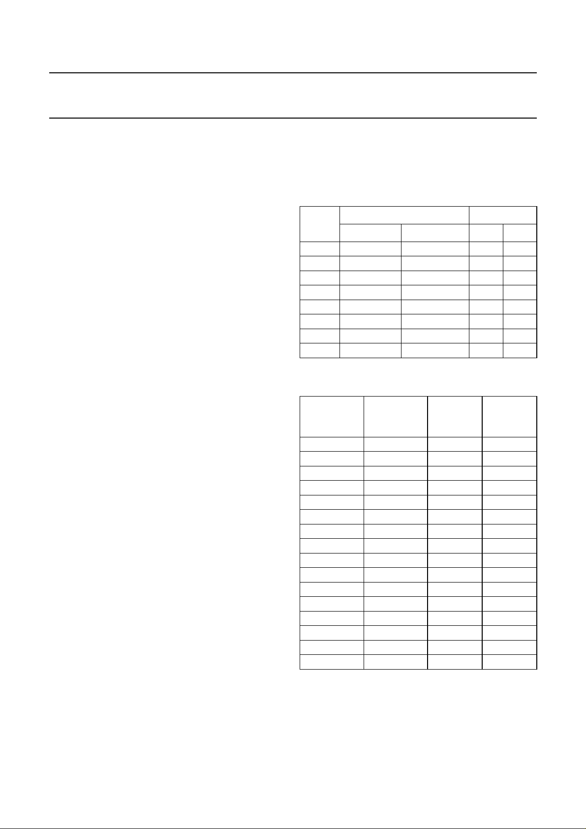
6.5 DTMF frequencies
Assuming an oscillator frequency f
DTMF standard frequencies can be implemented as
shown in Table 5.
xtal
-------------------------------23 x 2+()[]
; where 60 ≤ x ≤ 255.
=1⁄3× f
DTMF
= 3.58 MHz, the
xtal
is output
xtal
DTMF=fxtal
is
PCD3350A
The relationships between telephone keyboard symbols,
DTMF frequency pairs and the frequency register contents
are given in Table 6.
Table 5 DTMF standard frequencies and their
implementation; value = LGF, HGF contents
VALUE
(HEX)
DD 697 697.90 0.13 0.90
C8 770 770.46 0.06 0.46
B5 852 850.45 −0.18 −1.55
A3 941 943.23 0.24 2.23
7F 1209 1206.45 −0.21 −2.55
72 1336 1341.66 0.42 5.66
67 1477 1482.21 0.35 5.21
5D 1633 1638.24 0.32 5.24
Table 6 Dialling symbols, corresponding DTMF
TELEPHONE
KEYBOARD
SYMBOLS
0 (941, 1336) A3 72
1 (697, 1209) DD 7F
2 (697, 1336) DD 72
3 (697, 1477) DD 67
4 (770, 1209) C8 7F
5 (770, 1336) C8 72
6 (770, 1477) C8 67
7 (852, 1209) B5 7F
8 (852, 1336) B5 72
9 (852, 1477) B5 67
A (697, 1633) DD 5D
B (770, 1633) C8 5D
C (852, 1633) B5 5D
D (941, 1633) A3 5D
• (941, 1209) A3 7F
# (941, 1477) A3 67
FREQUENCY (Hz) DEVIATION
STANDARD GENERATED (%) (Hz)
frequency pairs and frequency register contents
DTMF FREQ.
PAIRS
(Hz)
LGF
VALUE
(HEX)
HGF
VALUE
(HEX)
1996 Dec 18 9
Philips Semiconductors Product specification
8-bit microcontroller with DTMF generator,
256 bytes EEPROM and real-time clock
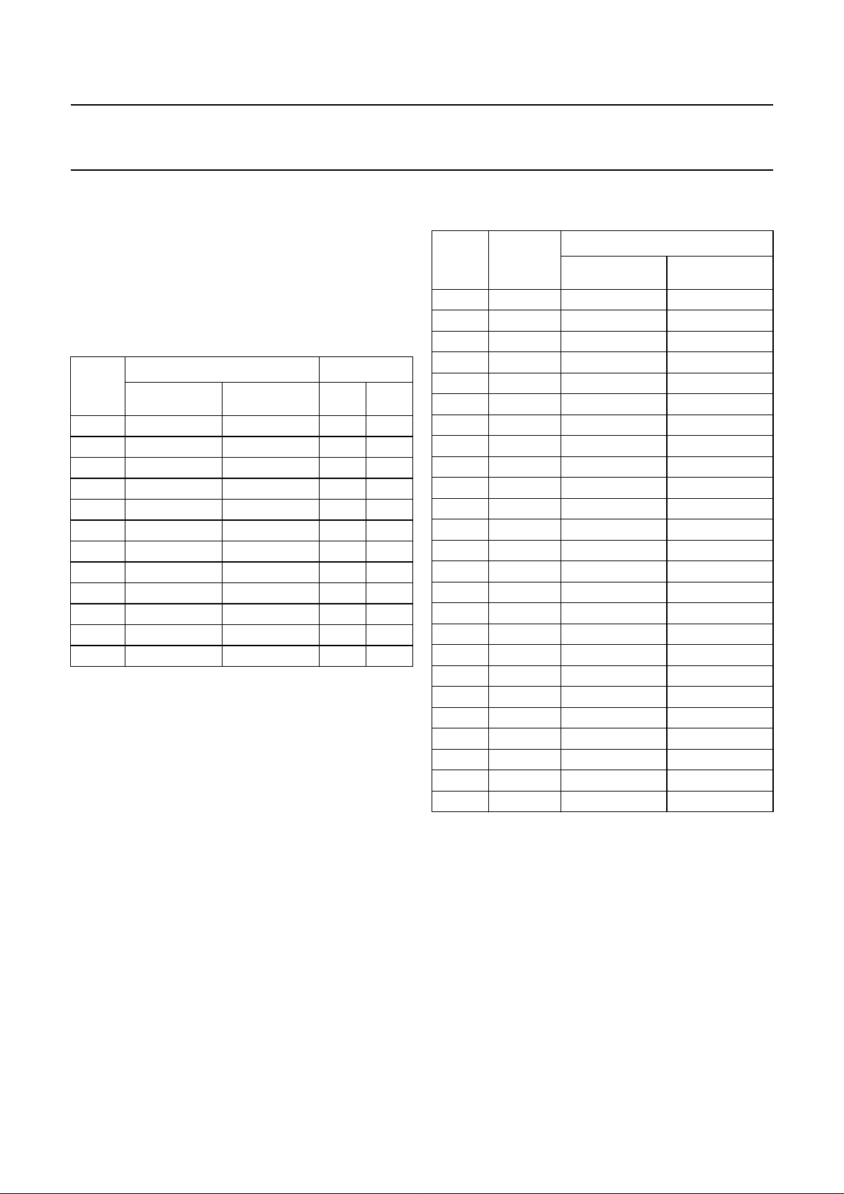
6.6 Modem frequencies
Again assuming an oscillator frequency f
the standard modem frequencies can be implemented as
in Table 7. It is suggested to define the frequency by the
HGF register while the LGF register contains 00H,
disabling Low Group Frequency generation.
Table 7 Standard modem frequencies and their
implementation
HGF
FREQUENCY (Hz) DEVIATION
VALUE
(HEX)
9D 980
82 1180
8F 1070
79 1270
80 1200
45 2200
76 1300
48 2100
5C 1650
52 1850
4B 2025
44 2225
MODEM GENERATED (%) (Hz)
(1)
(1)
(2)
(2)
(3)
(3)
(4)
(4)
(1)
(1)
(2)
(2)
978.82 −0.12 −1.18
1179.03 −0.08 −0.97
1073.33 0.31 3.33
1265.30 −0.37 −4.70
1197.17 −0.24 −2.83
2192.01 −0.36 −7.99
1296.94 −0.24 −3.06
2103.14 0.15 3.14
1655.66 0.34 5.66
1852.77 0.15 2.77
2021.20 −0.19 −3.80
2223.32 −0.08 −1.68
Notes
1. Standard is V.21.
2. Standard is Bell 103.
3. Standard is Bell 202.
4. Standard is V.23.
6.7 Musical scale frequencies
= 3.58 MHz,
xtal
PCD3350A
Table 8 Musical scale frequencies and their
implementation
HGF
NOTE
VALUE
(HEX)
D#5 F8 622.3 622.5
E5 EA 659.3 659.5
F5 DD 698.5 697.9
F#5 D0 740.0 741.1
G5 C5 784.0 782.1
G#5 B9 830.6 832.3
A5 AF 880.0 879.3
A#5 A5 923.3 931.9
B5 9C 987.8 985.0
C6 93 1046.5 1044.5
C#6 8A 1108.7 1111.7
D6 82 1174.7 1179.0
D#6 7B 1244.5 1245.1
E6 74 1318.5 1318.9
F6 6D 1396.9 1402.1
F#6 67 1480.0 1482.2
G6 61 1568.0 1572.0
G#6 5C 1661.2 1655.7
A6 56 1760.0 1768.5
A#6 51 1864.7 1875.1
B6 4D 1975.5 1970.0
C7 48 2093.0 2103.3
C#7 44 2217.5 2223.3
D7 40 2349.3 2358.1
D#7 3D 2489.0 2470.4
FREQUENCY (Hz)
STANDARD
(1)
GENERATED
Finally, two octaves of musical scale in steps of semitones
can be realized, again assuming an oscillator frequency
f
= 3.58 MHz (Table 8). It is suggested to define the
xtal
frequency by the HGF register while the LGF contains
00H, disabling Low Group Frequency generation.
1996 Dec 18 10
Note
1. Standard scale based on A4 @ 440 Hz.

Philips Semiconductors Product specification
8-bit microcontroller with DTMF generator,
256 bytes EEPROM and real-time clock
7 EEPROM AND TIMER 2 ORGANIZATION
The PCD3350A has 256 bytes of Electrically Erasable
Programmable Read Only Memory (EEPROM). Such
non-volatile storage provides data retention without the
need for battery backup. In telecom applications, the
EEPROM is used for storing redial numbers and for short
dialling of frequently used numbers. More generally,
EEPROM may be used for customizing microcontrollers,
such as to include a PIN code or a country code, to define
trimming parameters, to select application features from
the range stored in ROM.
The most significant difference between a RAM and an
EEPROM is that a bit in EEPROM, once written to a
logic 1, cannot be cleared by a subsequent write
operation. Successive write accesses actually perform a
logical OR with the previously stored information.
Therefore, to clear a bit, the whole byte must be erased
and re-written with the particular bit cleared. Thus, an
erase-and-write operation is the EEPROM equivalent of a
RAM write operation.
PCD3350A
Whereas read access times to an EEPROM are
comparable to RAM access times, write and erase access
times are much slower at 5 ms each. To make these
operations more efficient, several provisions are available
in the PCD3350A.
First, the EEPROM array is structured into 64 four-byte
pages (see Fig.4) permitting access to 4 bytes in parallel
(write page, erase/write page and erase page). It is also
possible to erase and write individual bytes.
Finally, the EEPROM address register provides
auto-incrementing, allowing very efficient read and write
accesses to sequential bytes.
To simplify the erase and write timing, the derivative 8-bit
down-counter (Timer 2) with reload register is provided.
In addition to EEPROM timing, Timer 2 can be used for
general real-time tasks, such as for measuring signal
duration and for defining pulse widths.
1996 Dec 18 11
 Loading...