

Philips PCD3349AT-107, PCD3349AT-144, PCD3349AP-107-3, PCD3349AP-117 Datasheet

DATA SH EET
Product specification
Supersedes data of 1996 Dec 18
File under Integrated Circuits, IC03
1998 May 11
INTEGRATED CIRCUITS
PCD3349A
8-bit microcontroller with
DTMF generator

1998 May 11 2
Philips Semiconductors Product specification
8-bit microcontroller with DTMF generator PCD3349A
CONTENTS
1 FEATURES
2 GENERAL DESCRIPTION
3 ORDERING INFORMATION
4 BLOCK DIAGRAM
5 PINNING INFORMATION
5.1 Pinning
5.2 Pin description
6 FREQUENCY GENERATOR
6.1 Frequency generator derivative registers
6.2 Frequency registers
6.3 DTMF frequencies
6.4 Modem frequencies
6.5 Musical scale frequencies
7 TIMING
8 RESET
9 STOP MODE
10 IDLE MODE
11 INSTRUCTION SET
12 SUMMARY OF MASK OPTIONS
13 LIMITING VALUES
14 HANDLING
15 DC CHARACTERISTICS
16 AC CHARACTERISTICS
17 PACKAGE OUTLINES
18 SOLDERING
18.1 Introduction
18.2 DIP
18.3 SO
19 DEFINITIONS
20 LIFE SUPPORT APPLICATIONS
1998 May 11 3
Philips Semiconductors Product specification
8-bit microcontroller with DTMF generator PCD3349A
1 FEATURES
• 8-bit CPU, ROM, RAM, I/O in a single 28-lead package
• 4-kbyte ROM
• 224-byte RAM
• Over 100 instructions (based on MAB8048) all of 1 or 2
cycles
• 20 quasi-bidirectional I/O port lines
• 8-bit programmable Timer/event counter 1
• 2 single-level vectored interrupts:
– external
– Timer/event counter 1
• Two test inputs, one of which also serves as the external
interrupt input
• DTMF tone generator
• Reference for supply and temperature-independent
TONE output
• Filtering for low output distortion (CEPT compatible)
• Power-on-reset
• Stop and Idle modes
• Supply voltage: 1.8 to 6 V (DTMF TONE output from
2.5 V)
• Low standby voltage of 1 V
• Low Stop mode current of 1 µA (typical)
• Clock frequency: 1 to 16 MHz (3.58 MHz for DTMF
suggested)
• Manufactured in silicon gate CMOS process.
2 GENERAL DESCRIPTION
The PCD3349A provides 4 kbytes of Program Memory,
224 bytes of RAM and 20 I/O lines.
The PCD3349A is a microcontroller which has been
designed primarily for telecom applications. It includes an
on-chip dual tone multi-frequency (DTMF) generator.
The instruction set is based on that of the MAB8048 and is
software compatible with the PCD33xxA family.
This data sheet details the specific properties of the
PCD3349A. The shared characteristics of the PCD33xxA
family of microcontrollers are described in the
“PCD33xxA
Family”
data sheet and also in
“Data Handbook IC03;
Section PCD33xxA Family”
, which should be read in
conjunction with this publication.
3 ORDERING INFORMATION
TYPE NUMBER
PACKAGE
NAME DESCRIPTION VERSION
PCD3349AP DIP28
plastic dual in-line package; 28 leads (600 mil)
SOT117-1
PCD3349AT SO28
plastic small outline package; 28 leads; body width 7.5 mm
SOT136-1
Philips Semiconductors Product specification
8-bit microcontroller with DTMF generator PCD3349A
1998 May 11 4
This text is here in white to force landscape pages to be rotated correctly when browsing through the pdf in the Acrobat reader.This text is here in
_white to force landscape pages to be rotated correctly when browsing through the pdf in the Acrobat reader.This text is here inThis text is here in
white to force landscape pages to be rotated correctly when browsing through the pdf in the Acrobat reader. white to force landscape pages to be ...
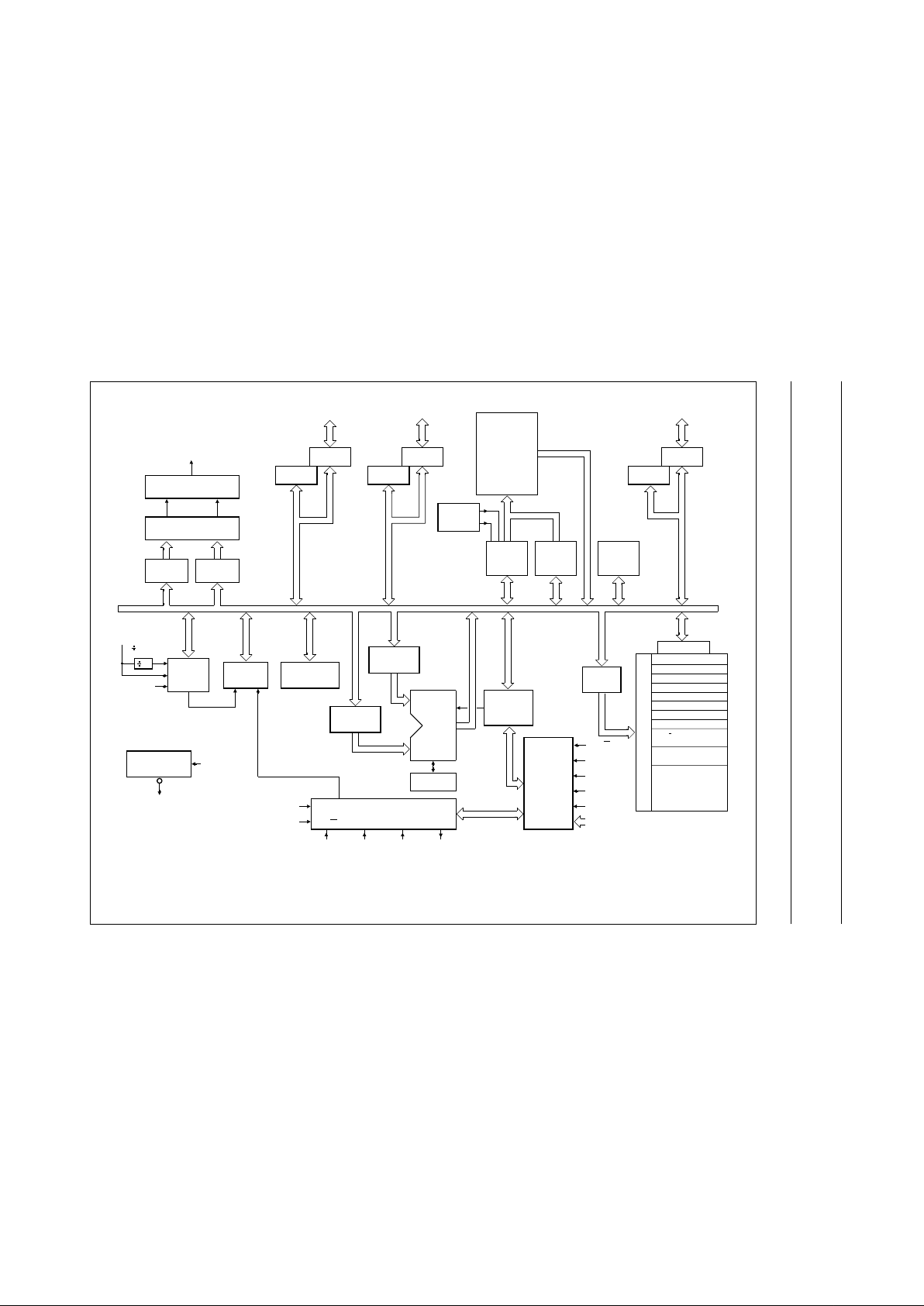
4 BLOCK DIAGRAM
handbook, full pagewidth
OSCILLATOR
MBG098
PORT 0
FLIP-FLOP
PORT 0
BUFFER
88
HIGHER
PROGRAM
COUNTER
LOWER
PROGRAM
COUNTER
PROGRAM
STATUS
WORD
MEMORY
BANK
FLIP-FLOPS
RESIDENT ROM
4 kbytes
DECODE
8
T1
8
8
5 888 8
8
P0.0 to P0.7
RAM
ADDRESS
REGISTER
ACCUMULATOR
TEMPORARY
REGISTER 1
PCD3349A
HGF
REGISTER
8
88
LGF
REGISTER
SINE WAVE
GENERATOR
TEMPORARY
REGISTER 2
ARITHMETIC
LOGIC UNIT
INSTRUCTION
REGISTER
&
DECODER
DECIMAL
ADJUST
CONTROL & TIMING
XTAL 2XTAL 1RESET
STOP
IDLE
INTERRUPT
INITIALIZE
CONDITIONAL
BRANCH
LOGIC
CE / T0
CE / T0
T1
TIMER
FLAG
CARRY
ACC
ACC BIT
TEST
RESIDENT RAM ARRAY
224 bytes
MULTIPLEXER
8 LEVEL STACK
(VARIABLE LENGTH)
OPTIONAL SECOND
REGISTER BANK
DATA STORE
D
E
C
O
D
E
REGISTER 0
REGISTER 1
REGISTER 2
REGISTER 3
REGISTER 4
REGISTER 5
REGISTER 6
REGISTER 7
PORT 1
FLIP-FLOP
PORT 1
BUFFER
P1.0 to P1.7
8
8
PORT 2
FLIP-FLOP
PORT 2
BUFFER
P2.0 to P2.3
4
4
TIMER/
EVENT
COUNTER
32
INTERNAL
CLOCK
FREQUENCY
30
8
88 8 8
INTERRUPT
LOGIC
timer interrupt
external interrupt
TONE
FILTER
POWER-ON-RESET
V
POR
RESET
Fig.1 Block diagram.
1998 May 11 5
Philips Semiconductors Product specification
8-bit microcontroller with DTMF generator PCD3349A
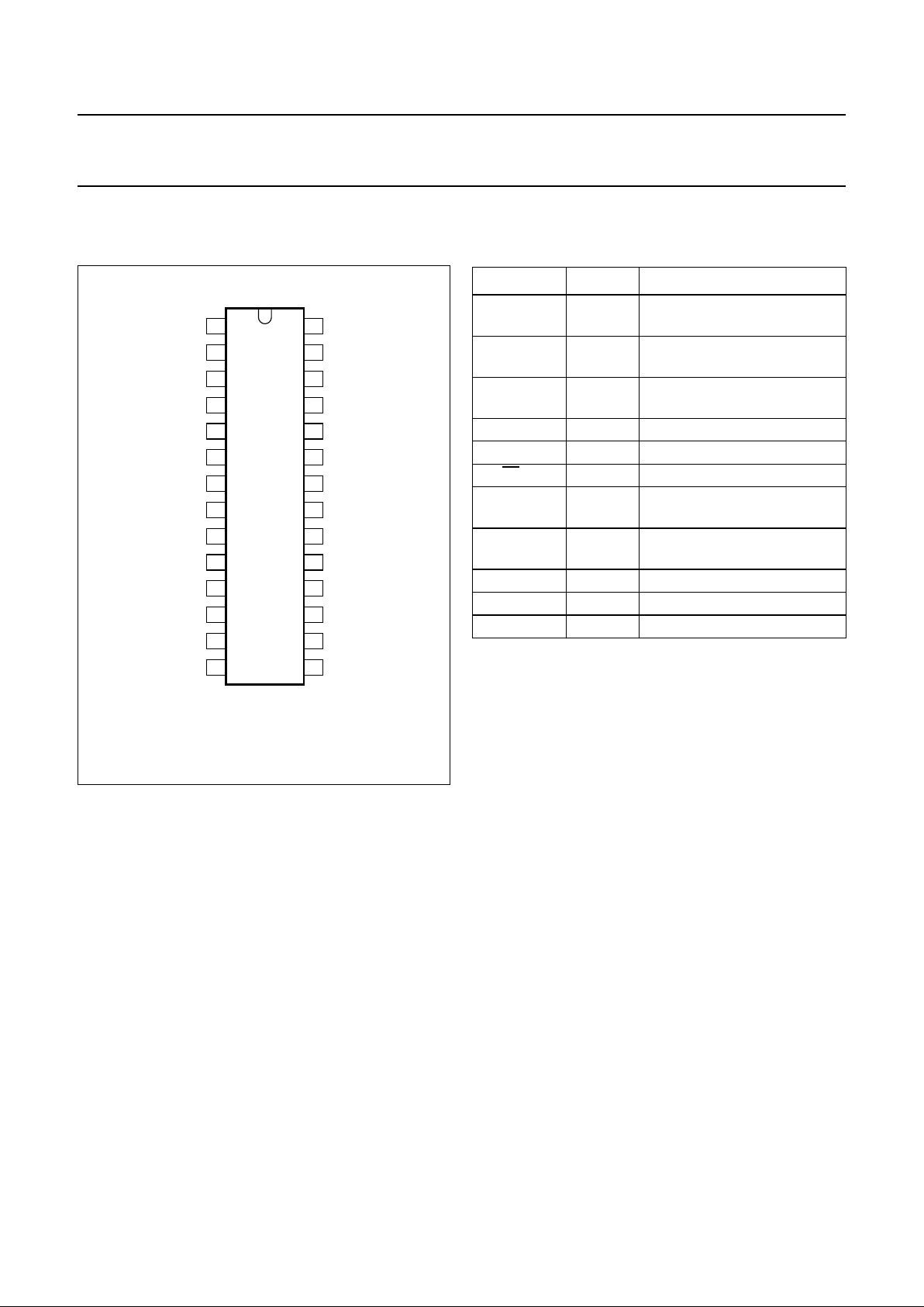
5 PINNING INFORMATION
5.1 Pinning
Fig.2 Pin configuration (SOT117-1 and SOT136-1).
handbook, halfpage
PCD3349A
MBG087
1
2
3
4
5
6
7
8
9
10
11
12
13
14
28
27
26
25
24
23
22
21
20
19
18
17
16
15
P0.1 P0.0
P2.3
P2.2
P2.1
V
DD
TONE
V
SS
P2.0
P1.7
P1.6
P1.5
P1.4
P1.3
P1.2
P0.2
P0.3
P0.4
P0.5
P0.6
P0.7
T1
XTAL1
XTAL2
RESET
P1.0
P1.1
CE/T0
5.2 Pin description
Table 1 SOT117-1 and SOT136-1 packages
SYMBOL PIN DESCRIPTION
P0.0 to P0.7 28, 1 to 7 Port 0: 8 quasi-bidirectional
I/O lines
T1 8 Test 1 or count input of 8-bit
Timer/event counter 1
XTAL1 9 crystal oscillator or external
clock input
XTAL2 10 crystal oscillator output
RESET 11 reset input
CE/
T0 12 Chip Enable or Test 0
P1.0 to P1.7 13 to 20 Port 1: 8 quasi-bidirectional
I/O lines
P2.0 to P2.3 21, 25,
26, 27
Port 2: 4 quasi-bidirectional
I/O lines
V
SS
22 ground
TONE 23 DTMF output
V
DD
24 positive supply voltage
1998 May 11 6
Philips Semiconductors Product specification
8-bit microcontroller with DTMF generator PCD3349A
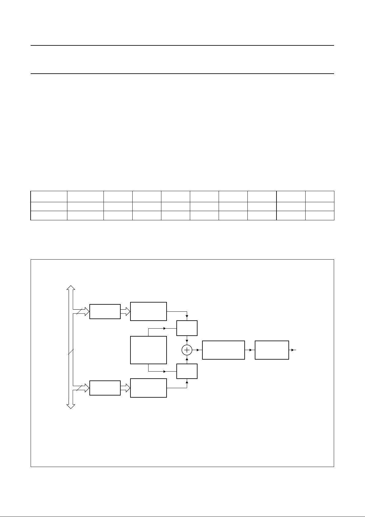
6 FREQUENCY GENERATOR
A versatile frequency generator section is provided (see
Fig.3). For normal operation, use a 3.58 MHz quartz
crystal or PXE resonator. The frequency generator
includes precision circuitry for dual tone multifrequency
(DTMF) signals, which is typically used for tone dialling
telephone sets.
The TONE output can alternatively issue twelve modem
frequencies for data rates between 300 and 1200 bits/s.
In addition to DTMF and modem frequencies, two octaves
of musical scale in steps of semitones are available.
6.1 Frequency generator derivative registers
Table 2 gives the derivative addresses, mnemonics and access types of the frequency generator derivative registers.
The addresses 03H to FFH are not used.
Table 2 Addresses of the frequency generator derivative registers
Notes
1. HGF = High Group Frequency; access type W.
2. LGF = Low Group Frequency; access type W.
ADDRESS REGISTER 7 6 5 4 3 2 1 0
01H HGF
(1)
H7 H6 H5 H4 H3 H2 H1 H0
02H LGF
(2)
L7 L6 L5 L4 L3 L2 L1 L0
Fig.3 Block diagram of the frequency generator section.
book, full pagewidth
HGF
REGISTER
MBG099
DIGITAL
SINE WAVE
SYNTHESIZER
8
SWITCHED-
CAPACITOR
BANDGAP
VOLTAGE
REFERENCE
DAC
DAC
LGF
REGISTER
DIGITAL
SINE WAVE
SYNTHESIZER
8
8 internal bus
SWITCHED-
CAPACITOR
LOW-PASS FILTER
RC LOW-PASS
FILTER
TONE
 Loading...