

Philips PCD3310AT, PCD3310P, PCD3310T, PCD3310AP Datasheet

INTEGRATED CIRCUITS
DATA SH EET
PCD3310; PCD3310A
Pulse and DTMF diallers with redial
Product specification
Supersedes data of 1996 May 06
File under Integrated Circuits, IC03
1996 Nov 21

Philips Semiconductors Product specification
Pulse and DTMF diallers with redial PCD3310; PCD3310A
CONTENTS
1 FEATURES
2 GENERAL DESCRIPTION
3 QUICK REFERENCE DATA
4 ORDERING INFORMATION
5 BLOCK DIAGRAM
6 PINNING
7 FUNCTIONAL DESCRIPTION
7.1 Power supply (VDD and VSS)
7.2 Clock oscillator (OSCI and OSCO)
7.3 Chip enable (CE)
7.4 Mode selection (PD/DTMF)
7.4.1 Pulse mode
7.4.2 DTMF mode
7.4.3 Mixed mode
7.5 Keyboard inputs/outputs
7.6 Flash duration control (FLD)
7.7 TONE output (DTMF mode)
7.8 Dial pulse and Flash output (DP/FLO)
7.9 Mute output (M1)
7.10 Mute output (M1)
7.11 Muting output (M2)
8 DIALLING PROCEDURES
8.1 Dialling
8.2 Redialling
8.3 Notepad
9 HANDLING
10 LIMITING VALUES
11 CHARACTERISTICS
12 TIMING CHARACTERISTICS
13 APPLICATION INFORMATION
14 PACKAGE OUTLINES
15 SOLDERING
15.1 Introduction
15.2 DIP
15.2.1 Soldering by dipping or by wave
15.2.2 Repairing soldered joints
15.3 SO
15.3.1 Reflow soldering
15.3.2 Wave soldering
15.3.3 Repairing soldered joints
16 DEFINITIONS
17 LIFE SUPPORT APPLICATIONS
1996 Nov 21 2

Philips Semiconductors Product specification
Pulse and DTMF diallers with redial PCD3310; PCD3310A
1 FEATURES
• Pulse, DTMF and ‘mixed mode’ dialling
• Mixed mode dialling: start with pulse dial, end with
DTMF dial (e.g. for control of DTMF user equipment via
a pulse network)
• 23-digit memory stores last number dialled, or number
noted during conversation (notepad)
• Redial of both PABX and external calls
• Supports 16 dial keys: 0 to 9, ∗, # A, B, C, and D
• Supports 4 function keys:
– Program (P) used to input notepad numbers
– Flash (FL) allows re-dialling without on-hook
– Redial (R) recalls and redialls stored number
– Change from pulse dial to DTMF dial in
mixed mode (>)
• DTMF timing:
– for manual dialling, maximum duration burst/pause
intervals are user-determined, but at least minimum
duration burst/pause intervals are ensured
– for redial, minimum duration burst/pause intervals are
used
• On-chip voltage reference for supply and temperature
independent tone output
• On-chip filtering for low output distortion
(CEPT compatible)
• On-chip oscillator uses low-cost 3.58 MHz (TV colour
burst) crystal or piezo resonator
• Uses standard single-contact or double-contact
(common left open) keyboard
• Keyboard entries fully debounced
• Flash (register recall) output.
2 GENERAL DESCRIPTION
The PCD3310 and PCD3310A are single-chip silicon gate
CMOS integrated circuits. They are dual-standard diallers
for pulse or dual tone multi-frequency (DTMF) dialling, with
on-chip oscillators suitable for use with 3.58 MHz crystals.
Input data is derived from any standard matrix keyboard
for dialling in either the pulse or DTMF mode.
Numbers up to 23 digits can be retained in RAM for
dialling/redialling.
3 QUICK REFERENCE DATA
SYMBOL PARAMETER CONDITIONS MIN. TYP. MAX. UNIT
V
DD
V
stb
I
DD(stb)
I
DD(conv)
I
DD(pulse)
I
DD(DTMF)
V
HG(RMS)
operating supply voltage 2.5 − 6.0 V
standby supply voltage 1.8 − 6.0 V
standby current (on hook) V
= 1.8 V − 1.4 4 µA
stb
operating current in conversation mode VDD=3V −−150 µA
operating current in pulse dialling mode VDD=3V −−200 µA
operating current in DTMF dialling mode VDD=3V − 0.6 0.9 mA
DTMF output voltage level for HIGH group
− 192 − mV
(RMS value)
V
LG(RMS)
DTMF output voltage level for LOW group
− 150 − mV
(RMS value)
G
v
voltage gain (pre-emphasis) of group − 2.1 − dB
THD total harmonic distortion −−25 − dB
T
amb
operating ambient temperature −25 − +70 °C
1996 Nov 21 3
Philips Semiconductors Product specification
Pulse and DTMF diallers with redial PCD3310; PCD3310A
4 ORDERING INFORMATION
Table 1 Package information
TYPE
NUMBER
PCD3310P DIP20 plastic dual in-line package; 20 leads (300 mil) SOT146-1
PCD3310AP DIP20 plastic dual in-line package; 20 leads (300 mil) SOT146-1
PCD3310T SO28 plastic small outline package; 28 leads; body width 7.5 mm SOT136-1
PCD3310AT SO28 plastic small outline package; 28 leads; body width 7.5 mm SOT136-1
Table 2 Functional options
TYPE
NUMBER
PCD3310P 67, 33 ms 2 : 1
PCD3310T 67, 33 ms 2 : 1
PCD3310AP 60, 40 ms 3 : 2
PCD3310AT 60, 40 ms 3 : 2
Notes
1. Pulse frequency 10 Hz, inter-digit pause (t
2. Note that the PCD3310P; 10T and the PCD3310AP; 10AT differ only in the break/make ratio in pulse dialling.
The break/make times equate to mark-to-space ratios of 2 : 1 and 3 : 2 respectively.
NAME DESCRIPTION VERSION
PULSE DIAL; BREAK/MAKE TIME (see notes 1 and 2)
) = 840 ms.
id
PACKAGE
MARK-TO-SPACE
RATIO
1996 Nov 21 4
Philips Semiconductors Product specification
Pulse and DTMF diallers with redial PCD3310; PCD3310A
5 BLOCK DIAGRAM
DD
V
(21)
DP/FLO
16
PD
(2)
PD/DTMF
2
DTMF
19
(27)
DTMF LOW GROUP
COUNTER/CONTROLLER
DAC
+
(5)
LOW
4
VSSTONE
3
(3)
OSCILLATOR
COUNTER
TIME BASE
RESET DELAY
(28)
(1)
MGE490
20
OSCOOSCI
1
handbook, full pagewidth
CODE CONVERTER
PD AND FLASH LOGIC
TIMING CONTROLLER
PCD3310 FAMILY
OUTPUT
DAC
HIGH
DTMF HIGH GROUP
COUNTER/CONTROLLER
V
VOLTAGE
REFERENCE
POINTER
COUNTER
CONTROLLER
ADDRESS
DECODING
MAIN
REGISTER
ref
READ/
WRITE
OUTPUT
ON
RESET
POWER
INPUT
REGISTER
TEMPORARY
LOGIC
CONTROL
KEYPAD
INTERFACE/LOGIC
(26)
(24)
(20)
(8)
(19)
(17)
(16)
(15)
(14)
(13)
(12)
(10)
(9)
(22)
18
(23)
17
15
5
14
13
12
11
10
9
8
7
6
M2
CE
M1
M1
FLD
CF/DMODE/FS
COL 4
COL 3
COL 2
COL 1
ROW 1
ROW 2
ROW 3
ROW 4
ROW 5
Fig.1 Block diagram.
1996 Nov 21 5
The pin numbers given in parenthesis refer to the PCD3310T.
Philips Semiconductors Product specification
Pulse and DTMF diallers with redial PCD3310; PCD3310A
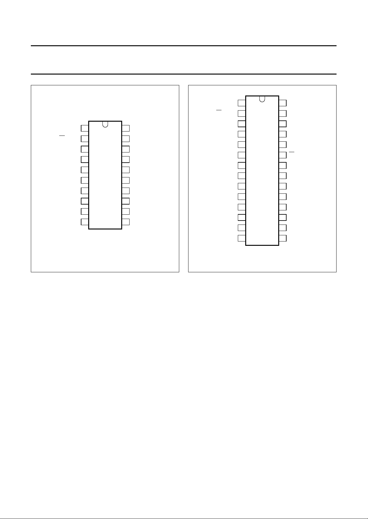
6 PINNING
PINS
SYMBOL
OSCI 1 1 I oscillator input
PD/DTMF 2 2 I select pin; pulse or DTMF dialling input
TONE 3 3 O single or dual tone frequency output
n.c. − 4 − not connected
V
SS
n.c. − 6 − not connected
n.c. − 7 − not connected
FLD 5 8 I/O flash duration control input/output
ROW 5 6 9 I/O scanning row 5 keyboard input/output
ROW 4 7 10 I/O scanning row 4 keyboard input/output
n.c. − 11 − not connected
ROW 3 8 12 I/O scanning row 3 keyboard input/output
ROW 2 9 13 I/O scanning row 2 keyboard input/output
ROW 1 10 14 I/O scanning row 1 keyboard input/output
COL 1 11 15 I sense column 1 keyboard input (with internal pull-up resistor)
COL 2 12 16 I sense column 2 keyboard input (with internal pull-up resistor)
COL 3 13 17 I sense column 3 keyboard input (with internal pull-up resistor)
n.c. − 18 − not connected
COL 4 14 19 I sense column 4 keyboard input (with internal pull-up resistor)
CF/DMODE/FS 15 20 O confidence tone/dialling mode/frequency select outputs
DP/FLO 16 21 O dialling pulse and flash output
M2 − 22 O muting output 2
M1 − 23 O muting output 1 (active LOW)
M1 17 24 O muting output 1
n.c. − 25 − not connected
CE 18 26 I chip enable input
V
DD
OSCO 20 28 O oscillator output
PCD3310P
PCD3310AP
4 5 P negative supply
19 27 P positive supply voltage
PCD3310T
PCD3310AT
TYPE DESCRIPTION
1996 Nov 21 6
Philips Semiconductors Product specification
Pulse and DTMF diallers with redial PCD3310; PCD3310A
handbook, halfpage
PD/DTMF
Fig.2 Pin configuration (DIP20 package).
OSCI
TONE
V
SS
FLD
ROW 5
ROW 4
ROW 3
ROW 2
ROW 1
1
2
3
4
5
PCD3310P
PCD3310AP
6
7
8
9
10
MGE489
OSCO
20
19
V
DD
18
CE
17
M1
16
DP/FLO
CF/DMODE/FS
15
COL 4
14
COL 3
13
COL 2
12
COL 1
11
handbook, halfpage
PD/DTMF
Fig.3 Pin configuration (SO28 package).
OSCI
TONE
n.c.
V
SS
n.c.
n.c.
FLD
ROW 5
ROW 4
n.c.
ROW 3
ROW 2
ROW 1
1
2
3
4
5
6
7
PCD3310T
PCD3310AT
8
9
10
11
12
13
MGE488
OSCO
28
V
27
DD
CE
26
n.c.
25
M1
24
23
M1
M2
22
21
DP/FLO
CF/DMODE/FS
20
COL 4
19
n.c.
18
COL 3
17
COL 2
16
1514
COL 1
7 FUNCTIONAL DESCRIPTION
References to ‘the device’ apply to both the PCD3310 and
the PCD3310A.
7.1 Power supply (V
The positive supply of the device (V
and VSS)
DD
) must meet the
DD
voltage requirements as indicated in Chapter 11.
To avoid undefined states of the device at power-on, an
internal reset circuit clears the control logic and counters.
If VDD drops below the minimum standby supply voltage of
1.8 V the power-on reset circuit inhibits redialling after
hook-off. The power-on reset signal has the highest
priority; it blocks and resets the device without delay
regardless of the state of chip enable input (CE).
7.2 Clock oscillator (OSCI and OSCO)
The timebase for the device for both pulse and DTMF
dialling is a crystal controlled on-chip oscillator which is
completed by connecting a 3.58 MHz crystal or ceramic
resonator between the OSCI and OSCO pins.
Recommended resonator type:
• 3.58 MHz PXE - Murata; CSA 3.58MG310VA.
7.3 Chip enable (CE)
The CE input enables the device and is used to initialize
the device. When CE is LOW it provides the static standby
condition. In this state the clock oscillator is disabled, all
registers and logic are reset with the exception of the redial
registers, Read Address Counter (RAC), Write Address
Counter (WAC) and Temporary Write Address Counter
(TWAC). The RAC points to the first digit of the last
number dialled, the WAC and TWAC point to the last
entered digits in the main and temporary registers
(see Fig.6). The keyboard input is inhibited, but data
previously entered is saved in the redial registers provided
is higher than V
V
DD
. The current drawn is I
stb
(standby
stb
current) and serves to retain data in the redial registers
during hook-on.
When CE is HIGH it activates the clock oscillator and the
device changes from static standby condition to the
conversation mode. The current consumption is I
DD(conv)
until the first digit is entered from the keyboard. Then a
dialling or redialling operation starts. The operating current
is I
DD(pulse)
if in the pulse dialling mode, or I
DD(DTMF)
if the
DTMF dialling mode is selected.
1996 Nov 21 7
Philips Semiconductors Product specification
Pulse and DTMF diallers with redial PCD3310; PCD3310A
If the CE input is taken to a LOW level for longer than time
period trd (see Figs 11 and 12 and Chapter 12) an internal
reset pulse will be generated at the end of the trd period.
The system changes to the static standby state. Short CE
pulses of < trd will not affect the operation of the device and
reset pulses are not produced.
7.4 Mode selection (
7.4.1 P
ULSE MODE
PD/DTMF)
If PD/DTMF = VSS the pulse mode is selected. Entries of
non-numeric keys are neglected, they are neither stored in
the redial register nor transmitted.
7.4.2 DTMF
MODE
If PD/DTMF = VDD the dual tone multi-frequency dialling
mode is selected. Each non-function key activated
corresponds to a combination of two tones, one of four
LOW and one of four HIGH frequencies, corresponding to
the key’s row and column in the keyboard matrix.
See Fig.4 and Table 3. The frequencies are transmitted
with a constant amplitude, regardless of power supply
variations. Harmonic content is filtered out thus meeting
the CEPT recommendations.
entries are debounced on both the leading and trailing
edges for approximately time period t
as shown in
e
Figs 11, 12, 13 and 14. Each entry is tested for validity.
When a key is depressed, keyboard scanning starts and
only returns to the sense mode after release of that key.
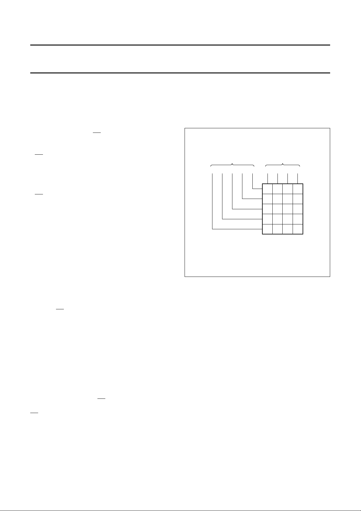
handbook, halfpage
54321 1234
MGE491
ROWS
COLUMNS
123
45
7
∗
PFLR
6
9
8
#
0
KEYBOARD
A
B
C
D
>
The transmission time is calibrated for redial. In manual
operation the duration of bursts and pauses is the actual
key depression time, but not less than the minimum
transmission time (tt) or minimum pause time (tp).
7.4.3 M
IXED MODE
When the PD/DTMF pin is open-circuit the mixed mode is
selected. After activation of CE or FL (Flash) the device
starts as a pulse dialler and remains in this state until a
non-numeric dial key (A, B, C, D,∗, #) or the function key >
is activated. Pressing a non-numeric dial key causes the
corresponding DTMF tones to be output, and any
subsequent dialling to be in DTMF mode. Pressing >
causes no output tones, but any subsequent dialling is in
DTMF mode. The > key should be used if the first DTMF
output required is numeric. The device remains in DTMF
dial mode until FL is activated or after a static standby
condition when CE is re-activated.
A connection between the PD/DTMF pin and VDD also
initiates DTMF dialling. Chip enable, FL or a connection of
PD/DTMF pin to VSS sets the device back to pulse dialling.
7.5 Keyboard inputs/outputs
Fig.4 Keyboard organization.
ROW 5 of the keyboard contains the following function
keys:
• P = memory clear and programming (notepad)
• FL = flash or register recall
• R = redial
• > = change of dial mode from pulse to DTMF in mixed
dialling mode.
In the pulse dialling mode the valid keys are the
10 numeric dial keys (0 to 9). The non-numeric dial keys
(A, B, C, D, ∗, #) have no effect on the dialling or the redial
storage. Valid function keys are P, R and FL.
In the DTMF mode all dial keys are valid. They are
transmitted as a dual tone combination and at the same
time stored in the redial register. Valid function keys are P,
FL and R.
In the mixed mode all key entries are valid and executed
accordingly.
The sense column inputs COL 1 to COL 4 and the
scanning row outputs ROW 1 to ROW 5 of the device are
connected to the keyboard as shown in Fig.4. All keyboard
1996 Nov 21 8

Philips Semiconductors Product specification
Pulse and DTMF diallers with redial PCD3310; PCD3310A
7.6 Flash duration control (FLD)
Flash (or register recall) is activated by the FL key and can
be used in DTMF and pulse dialling modes.
The FL key has the same effect as placing the telephone
‘on-hook’ for a calibrated time. Pressing the FL key will
produce a timed line-break of 100 ms (min.) at the DP/FLO
output. During the conversation mode pressing FL also
acts as a chip enable. The flash pulse duration (tFL) is
calibrated and can be prolonged with an external resistor
and capacitor connected to the FLD input/output (see
Fig.5). The flash pulse resets the Read Address Counter
(RAC) to the address of the first entered digit of the last
number dialled. Subsequent redial is possible (see Fig.9).
The counter of the reset delay time is held for a period of
.
t
FL
7.7 TONE output (DTMF mode)
The single and dual tones which are provided at the TONE
output are filtered by an on-chip switched capacitor filter,
followed by an on-chip active RC low-pass filter. Hence,
the total harmonic distortion of the DTMF tones meets the
CEPT recommendations. The tone output has the
following states:
• tone OFF; 3-state
• tone ON; the associated frequencies are superimposed
1
on a DC level of
⁄2VDD.
When the DTMF mode is selected output tones are timed
in manual dialling with a minimum duration of bursts and
pauses, and in redial with a calibrated timing. Single tones
may be generated for test purposes (CE = HIGH). Each
row and column has one corresponding frequency.
High group frequencies are generated by connecting the
column to V
and LOW group frequencies are generated
SS
by forcing the row to VDD. The single tone frequency will be
transmitted during activation time, but it is neither
calibrated nor stored.
An on-chip reference voltage provides output tone levels
independent of the supply voltage. Table 3 shows the
frequency tolerance of the output tones for DTMF
signalling.
dbook, full pagewidth
(a) Flash duration control circuit.
(b) Flash pulse timing. t
FLRC
≈ R × C.
60
nA
FLD
(a)
R
FLO
C
Fig.5 Flash pulse duration setting.
1996 Nov 21 9
(b)
t
FLRC
MGE492
t
FL
 Loading...