

Philips PCB8517 Datasheet
INTEGRATED CIRCUITS
DATA SH EET
PCB8517
Stand-alone OSD for monitor
applications
Objective specification
File under Integrated Circuits, IC02
1997 Mar 03

Philips Semiconductors Objective specification
Stand-alone OSD for monitor applications PCB8517
FEATURES
Interface with microcontroller
• 3-wire high speed (maximum 2.5 Mbits/s) serial
interface with three types of transmission sequence.
On-Screen Display (OSD)
• On-chip PLL oscillator to generate the OSD dot clock
frequency which is 384 × horizontal sync frequency
• Horizontal sync frequency range of 10 to 100 kHz
• 10 rows of 24 characters display buffer
• 128 character fonts
• 12 × 16 character matrix
• Programmable height of displayed character (from
16 to 63 scan-lines); frame basis
• 4 types of character size; single/double character
height/width; row basis
• Horizontal starting position: 32 different positions
(6 dots for each step)
• Vertical starting position: 64 different positions
(4 scan-lines for each step)
• 8 foreground character colours: selection of only 2 out of
the 8 (outside the window) and 4 out of the of 8 (in the
window) in the same row
• 3 character shadowing modes:
– No shadow
– Shadowing
– Bordering shadow
• 3 fully programmable background windows with
overlapping capability and presetting priorities (for
multi-level application). The window colour can be
selected from 1 out of 8
• Half tone in background window supported
• Single 5 V power supply
• Available in DIP16 package.
GENERAL DESCRIPTION
The PCB8517 is a stand-alone OSD which is used to
display the adjustment/status information on the screen of
an auto-sync monitor for menu driving application.
The display operation of the device is controlled by a
microcontroller which programs the internal 273 bytes of
RAM via a 3-wire high-speed serial interface. The on-chip
PLL oscillator and programmable character height are
used to keep the same character size displayed on the
screen in different display modes, VGA, SVGA and XGA
for example.
The OSD of the PCB8517 provides display buffers of
10 rows with 24 characters each. These display buffers
can select from 128 customized character fonts (with
12 × 16 bit resolution) to be displayed. The characters
displayed on the screen can be specified double height,
double width, different colour and with/without shadowing.
Three positional background windows are provided for
multi-level application.
ORDERING INFORMATION
TYPE
NUMBER
PCB8517P DIP16 plastic dual in-line package; 16 leads (300 mil) SOT38-4
1997 Mar 03 2
NAME DESCRIPTION VERSION
PACKAGE
Philips Semiconductors Objective specification
Stand-alone OSD for monitor applications PCB8517
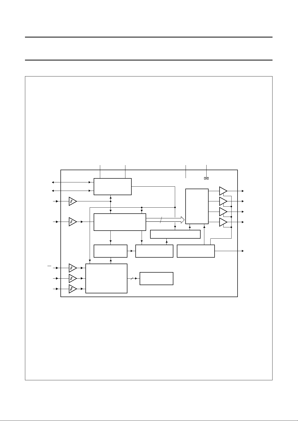
BLOCK DIAGRAM
handbook, full pagewidth
VCO
BIAS
HFLB
VFLB
EN
SDI
SCK
V
DDA
4
2
3
5
10
6
7
8
+
OSCILLATOR
−
DISPLAY CONTROL
DISPLAY BUFFER
24 × 10 RAM
HIGH SPEED SERIAL
I/O INTERFACE
PLL
V
SSA
1
CHARACTER FONTS
3
VCLK
4
12-STAGE SHIFT REGISTER
128 FONT ROM
CONTROL
REGISTERS
V
DDD
916
WINDOW AND
FRAME CONTROL
COLOUR
ENCODER
V
SSD
OSDEN
15
RED
14
GREEN
13
BLUE
12
FB
11
HTONE
MGD762
Fig.1 Block diagram.
1997 Mar 03 3

Philips Semiconductors Objective specification
Stand-alone OSD for monitor applications PCB8517
PINNING
SYMBOL PIN DESCRIPTION
V
SSA
VCO 2 DC control voltage input/output to regulate the internal PLL oscillator frequency; a low-pass filter
BIAS 3 bias input/output to regulate the bias current of internal current control oscillator to resonate at a
V
DDA
HFLB 5 horizontal sync input signal from flyback circuit with negative polarity
EN 6 active LOW input to enable serial interface
SDI 7 data input of serial interface
SCK 8 clock input of serial interface
V
DDD
VFLB 10 vertical sync input signal from flyback circuit with negative polarity
HTONE 11 half tone control which outputs a logic 1 during windowing except characters are displayed; it is
FB 12 fast blanking output of OSD; active HIGH and high impedance when OSD is disabled
BLUE 13 blue colour output of OSD; active HIGH and high impedance when OSD is disabled
GREEN 14 green colour output of OSD; active HIGH and high impedance when OSD is disabled
RED 15 red colour output of OSD; active HIGH and high impedance when OSD is disabled
V
SSD
1 analog ground
circuit is connected to this pin
specific dot frequency
4 analog power supply
9 digital power supply
used to lower the external RED, GREEN and BLUE amplifier gain to achieve a transparent
windowing effect
16 digital ground
handbook, halfpage
V
SSA
VCO
BIAS
V
DDA
HFLB
SDI
SCK
EN
1
2
3
4
5
6
7
8
PCB8517
MGD760
16
15
14
13
12
11
10
9
V
SSD
RED
GREEN
BLUE
FB
HTONE
VFLB
V
DDD
Fig.2 Pin configuration.
1997 Mar 03 4

Philips Semiconductors Objective specification
Stand-alone OSD for monitor applications PCB8517
FUNCTIONAL DESCRIPTION
3-wire high speed serial interface (HSSI)
The 3-wire (
EN, SDI and SCK) high speed serial interface
of the PCB8517 is write only and is used to write data from
the microcontroller to the internal 273 bytes of RAM (see
Section “Internal RAM organization (see Fig.4)”) to control
the OSD. The RAM is organized into 11 rows of
32 columns (see Fig.4) and can be programmed by three
types of sequence (see Section “Data sequence and
format”).
ATA PROTOCOL
D
Figure 3 shows the protocol of HSSI. To initiate HSSI
transmission, pin EN must be LOW to enable the
PCB8517 to accept data. The EN input must be pulled
LOW prior to the occurrence of SCK and remain LOW until
after the last SCK clock pulse. The rising edge of SCK
facilitates the input data of SDI being shifted into an 8-bit
shift register. When the shift register is full this data will be
loaded into a row address register, column address
register or into one of the internal RAM bytes.
Table 1 shows the switching characteristics when the
HFLB pin has a pulse presented, but when there is no
horizontal sync pulse present on the HFLB pin, the
transmission bit rate will be slowed down to 500 kbit/s.
Table 1 Switching characteristics (under operating
conditions)
SYMBOL PARAMETER MIN. MAX. UNIT
t
su(EN)
t
h(EN)
t
SCKL
t
SCKH
t
su(SDI)
t
h(SDI)
EN to SCK set-up time 200 − ns
EN to SCK hold time 100 − ns
SCK LOW time 200 − ns
SCK HIGH time 200 − ns
SDI data set-up time 200 − ns
SDI data hold time 100 − ns
handbook, full pagewidth
EN
SCK
SDI
t
su(EN)
B7
MSB
t
SCKH
first byte
t
SCKL
t
su(SDI)
t
h(SDI)
B0 B7B7 B0 B7 B0
LSB
last byte
Fig.3 3-wire serial interface protocol.
t
h(EN)
MGD764
1997 Mar 03 5

Philips Semiconductors Objective specification
Stand-alone OSD for monitor applications PCB8517
DATA SEQUENCE AND FORMAT
The PCB8517 provides the following 3 types of
transmission sequence:
• Sequence A: R ⇒ CA ⇒ D ⇒ R ⇒ CA ⇒ D etc.
• Sequence B: R ⇒ CA ⇒ D ⇒ CA ⇒ D ⇒ CA ⇒ D etc.
• Sequence C: R ⇒ CB ⇒ D ⇒ D ⇒ D ⇒ D etc.
Where: R = row address,
CA = column address A, CB = column address B,
D = data of RAM.
The column address will be increased by 1 automatically
after each bit of data has been stored into the RAM.
In sequence C, if the column address of the last data is
1FH, the row address will also be increased by 1.
The sequence A is particularly suitable for updating small
amounts of data between different rows. However, if the
current information byte has the same row address as the
previous one, sequence B is recommended. For a greater
information update, such as a power-up situation,
sequence C should be used.
Table 2 Data format
ADDRESS
B7 B6 B5 B4 B3 B2 B1 B0
Row address 1 X X X R3 R2 R1 R0
Column address A 0 0 X C4 C3 C2 C1 C0
Column address B 0 1 X C4 C3 C2 C1 C0
Bit B7 in Table 2 is used to distinguish between row or
column address and bit B6 is used to distinguish between
column address A or B. When A or B sequence is
transmitted, the column address should be formatted as
column address A, and the data format of column
address B is used for sequence C. There are some
limitations on using mixed formats during a single
transmission, for example when pin
LOW once.
Allowed:
• From A to B or C
• From B to A.
Not allowed:
• From C to A or B.
DATA BYTE
(1)
EN has been pulled to
Note
1. X = don’t care.
Internal RAM organization (see Fig.4)
The internal RAM is addressed with rows 0 to 10 and columns 0 to 31. The OSD character display buffers are located in
columns 0 to 23 of rows 0 to 9. Each display buffer contains a character ROM address and the colour control bit
corresponding to a display location on the monitor screen.
Each row data is associated with two control registers which are located at columns 30 and 31 of their respective row.
Also three window control registers for three windows together with three frame control register occupy the first
13 columns of row 10.
1997 Mar 03 6
Philips Semiconductors Objective specification
Stand-alone OSD for monitor applications PCB8517
handbook, full pagewidth
0
ROW CHARACTER DISPLAY BUFFERS RESERVED
9
WINDOW 1
10
CONTROL
02356891213 31
WINDOW 2
CONTROL
WINDOW 3
CONTROL
COLUMN
230 24 29 30 31
FRAME
CONTROL
Fig.4 Internal RAM map.
DISPLAY BUFFERS
ROW
CONTROL
RESERVED
MGD763
Table 3 Display buffers; see Table 4
DATA BYTE
BIT 7 BIT 6 BIT 5 BIT 4 BIT 3 BIT 2 BIT 1 BIT 0
CCS0 CA6 CA5 CA4 CA3 CA2 CA1 CA0
Table 4 Explanation of Table 3
BIT NAME DESCRIPTION
7 CCS0 This bit defines the characters colour. When the character has no window background
with it, colour 0 is selected if CCS0 = 0, otherwise colour 1 is selected. When the
character is inside a window and the CCS1 bit of the corresponding windows control
register is 0, the colour selection is the same as no window background, and if
CCS1 = 1, colour 2 is selected when CCS0 = 0, otherwise colour 3 is selected.
6 to 0 CA6 to CA0 These 7 bits define 1 of 128 character symbols to be displayed in this position.
1997 Mar 03 7
Philips Semiconductors Objective specification
Stand-alone OSD for monitor applications PCB8517
ROW CONTROL REGISTERS
Table 5 Column 30
DATA BYTE
BIT 7 BIT 6 BIT 5 BIT 4 BIT 3 BIT 2 BIT 1 BIT 0
R0 G0 B0 R1 G1 B1 CHS CWS
Table 6 Explanation of Table 5
BIT NAME DESCRIPTION
7 to 5 R0, G0, B0 colour definition of colour 0
4 to 2 R1, G1, B1 colour definition of colour 1
1 CHS This bit defines the height of the display character; when CHS = 1 double height is
selected.
(1)
0 CWS This bit defines the width of the display character; when CWS = 1 double width
selected.
is
Note
1. When the display row is selected to be double width, only even column characters will be displayed on the screen
and the odd column characters will not appear.
Table 7 Column 31
DATA BYTE
BIT 7 BIT 6 BIT 5 BIT 4 BIT 3 BIT 2 BIT 1 BIT 0
R2 G2 B2 R3 G3 B3 reserved
Table 8 Explanation of Table 7
BIT NAME DESCRIPTION
7 to 5 R2, G2, B2 colour definition of colour 2
4 to 2 R3, G3, B3 colour definition of colour 3
WINDOW CONTROL REGISTERS
There are three control registers for each window. Window 1 occupies columns 0 to 2 of row 10, columns 3 to 5 of
row 10 are occupied by window 2 and columns 6 to 8 of row 10 are occupied by window 3. If window overlapping occurs,
the highest priority window will cover the lowest. Window 1 has the highest priority and window 3 the lowest.
Table 9 Columns 0, 3 and 6 of row 10
DATA BYTE
BIT 7 BIT 6 BIT 5 BIT 4 BIT 3 BIT 2 BIT 1 BIT 0
MSB row start address LSB MSB row end address LSB
1997 Mar 03 8
 Loading...