

Philips PCA80C31BH3-16P, PCA80C51BH-3P, PCA80C51BH-3WP, PCB80C31-2A, PCB80C31-2N Datasheet
...
80C31/80C51/87C51
CMOS single-chip 8-bit microcontrollers
Product specification 1996 Aug 16
INTEGRATED CIRCUITS
IC20 Data Handbook
Philips Semiconductors Product specification
80C31/80C51/87C51CMOS single-chip 8-bit microcontrollers
2
1996 Aug 16 853–0169 17187
DESCRIPTION
The Philips 80C31/80C51/87C51 is a high-performance
microcontroller fabricated with Philips high-density CMOS
technology. The CMOS 8XC51 is functionally compatible with the
NMOS 8031/8051 microcontrollers. The Philips CMOS technology
combines the high speed and density characteristics of HMOS with
the low power attributes of CMOS. Philips epitaxial substrate
minimizes latch-up sensitivity.
The 8XC51 contains a 4k × 8 ROM (80C51) EPROM (87C51), a 128
× 8 RAM, 32 I/O lines, two 16-bit counter/timers, a five-source,
two-priority level nested interrupt structure, a serial I/O port for either
multi-processor communications, I/O expansion or full duplex UART,
and on-chip oscillator and clock circuits.
In addition, the device has two software selectable modes of power
reduction—idle mode and power-down mode. The idle mode freezes
the CPU while allowing the RAM, timers, serial port, and interrupt
system to continue functioning. The power-down mode saves the
RAM contents but freezes the oscillator, causing all other chip
functions to be inoperative.
FEATURES
•8031/8051 compatible
– 4k × 8 ROM (80C51)
– 4k × 8 EPROM (87C51)
– ROMless (80C31)
– 128 × 8 RAM
– Two 16-bit counter/timers
– Full duplex serial channel
– Boolean processor
•Memory addressing capability
– 64k ROM and 64k RAM
•Power control modes:
– Idle mode
– Power-down mode
•CMOS and TTL compatible
•Five speed ranges at V
CC
= 5V
– 12MHz
– 16MHz
– 24MHz
– 33MHz
•Five package styles
•Extended temperature ranges
•OTP package available
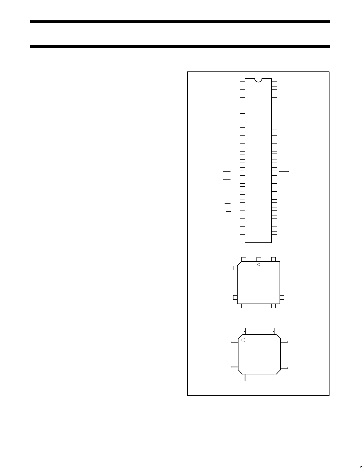
PIN CONFIGURATIONS
1
2
3
4
5
6
7
8
9
10
11
12
13
14
15
16
17
18
19
20
21
22
23
24
25
26
27
28
29
30
31
32
33
34
35
36
37
38
39
40
P1.0
P1.1
P1.2
P1.3
P1.4
P1.5
P1.6
RST
RxD/P3.0
TxD/P3.1
INT0
/P3.2
INT1
/P3.3
T0/P3.4
T1/P3.5
P1.7
WR
/P3.6
RD
/P3.7
XTAL2
XTAL1
V
SS
P2.0/A8
P2.1/A9
P2.2/A10
P2.3/A11
P2.4/A12
P2.5/A13
P2.6/A14
P2.7/A15
PSEN
ALE/PROG
EA/V
PP
P0.7/AD7
P0.6/AD6
P0.5/AD5
P0.4/AD4
P0.3/AD3
P0.2/AD2
P0.1/AD1
P0.0/AD0
V
CC
CERAMIC
AND
PLASTIC
DUAL
IN-LINE
PACKAGE
CERAMIC
AND
PLASTIC
LEAD
CHIP
CARRIER
6 1 40
7
17
39
29
18 28
PLASTIC
QUAD
FLAT
PACK
44
34
1
11
33
23
12 22
SU00001
SEE PAGE 3 FOR QFP AND LCC PIN FUNCTIONS.

Philips Semiconductors Product specification
80C31/80C51/87C51CMOS single-chip 8-bit microcontrollers
1996 Aug 16
3
CERAMIC AND PLASTIC LEADED CHIP CARRIER
PIN FUNCTIONS
LCC
6 1 40
7
17
39
29
18 28
Pin Function
1 NC*
2 P1.0
3 P1.1
4 P1.2
5 P1.3
6 P1.4
7 P1.5
8 P1.6
9 P1.7
10 RST
11 P3.0/RxD
12 NC*
13 P3.1/TxD
14 P3.2/INT0
15 P3.3/INT1
Pin Function
16 P3.4/T0
17 P3.5/T1
18 P3.6/WR
19 P3.7/RD
20 XTAL2
21 XTAL1
22 V
SS
23 NC*
24 P2.0/A8
25 P2.1/A9
26 P2.2/A10
27 P2.3/A11
28 P2.4/A12
29 P2.5/A13
30 P2.6/A14
Pin Function
31 P2.7/A15
32 PSEN
33 ALE/PROG
34 NC*
35 EA
/V
PP
36 P0.7/AD7
37 P0.6/AD6
38 P0.5/AD5
39 P0.4/AD4
40 P0.3/AD3
41 P0.2/AD2
42 P0.1/AD1
43 P0.0/AD0
44 V
CC
SU00002
* DO NOT CONNECT
PLASTIC QUAD FLAT PACK
PIN FUNCTIONS
Pin Function
1 P1.5
2 P1.6
3 P1.7
4 RST
5 P3.0/RxD
6 NC*
7 P3.1/TxD
8 P3.2/INT0
9 P3.3/INT1
10 P3.4/T0
11 P3.5/T1
12 P3.6/WR
13 P3.7/RD
14 XTAL2
15 XTAL1
Pin Function
16 V
SS
17 NC*
18 P2.0/A8
19 P2.1/A9
20 P2.2/A10
21 P2.3/A11
22 P2.4/A12
23 P2.5/A13
24 P2.6/A14
25 P2.7/A15
26 PSEN
27 ALE/PROG
28 NC*
29 EA
/V
PP
30 P0.7/AD7
Pin Function
31 P0.6/AD6
32 P0.5/AD5
33 P0.4/AD4
34 P0.3/AD3
35 P0.2/AD2
36 P0.1/AD1
37 P0.0/AD0
38 V
CC
39 NC*
40 P1.0
41 P1.1
42 P1.2
43 P.13
44 P1.4
PQFP
44 34
1
11
33
23
12 22
SU00003
* DO NOT CONNECT
LOGIC SYMBOL
PORT 0
PORT 1PORT 2
PORT 3
ADDRESS AND
DATA BUS
ADDRESS BUS
SECONDARY FUNCTIONS
RxD
TxD
INT0
INT1
T0
T1
WR
RD
RST
EA
/V
PP
PSEN
ALE/PROG
V
SS
V
CC
XTAL1
XTAL2
SU00004

Philips Semiconductors Product specification
80C31/80C51/87C51CMOS single-chip 8-bit microcontrollers
1996 Aug 16
4
ORDERING INFORMATION
PHILIPS NORTH AMERICA
EPROM
DRAWING
NUMBER
ROMless ROM
DRAWING
NUMBER
TEMPERATURE RANGE oC
AND PACKAGE
1
Freq
MHz
SC87C51CCF40 0590B 0 to +70, Ceramic Dual In-line Package, UV 3.5 to 12
SC87C51CCK44 1472A 0 to +70, Ceramic Leaded Chip Carrier, UV 3.5 to 12
SC87C51CCN40
SOT129-1
SC80C31BCCN40 SC80C51BCCN40
SOT129-1
0 to +70, Plastic Dual In-line Package, OTP 3.5 to 12
SC87C51CCA44 SOT187-2 SC80C31BCCA44 SC80C51BCCA44
SOT187-2
0 to +70, Plastic Leaded Chip Carrier, OTP 3.5 to 12
SC87C51CCB44
SOT307-2
SC80C31BCCB44 SC80C51BCCB44 SOT307-2 0 to +70, Plastic Quad Flat Pack, OTP 3.5 to 12
SC87C51ACF40 0590B –40 to +85, Ceramic Dual In-line Package, UV 3.5 to 12
SC87C51ACN40
SOT129-1
SC80C31BACN40 SC80C51BACN40
SOT129-1
–40 to +85, Plastic Dual In-line Package, OTP 3.5 to 12
SC87C51ACA44 SOT187-2 SC80C31BACA44 SC80C51BACA44 SOT187-2 –40 to +85, Plastic Leaded Chip Carrier, OTP 3.5 to 12
SC87C51ACB44 SOT307-2 SC80C31BACB44 SC80C51BACB44 SOT307-2 –40 to +85, Plastic Quad Flat Pack, OTP 3.5 to 12
SC87C51CGF40 0590B 0 to +70, Ceramic Dual In-line Package, UV 3.5 to 16
SC87C51CGK44 1472A 0 to +70, Ceramic Leaded Chip Carrier, UV 3.5 to 16
SC87C51CGN40
SOT129-1
SC80C31BCGN40 SC80C51BCGN40
SOT129-1
0 to +70, Plastic Dual In-line Package, OTP 3.5 to 16
SC87C51CGA44 SOT187-2 SC80C31BCGA44 SC80C51BCGA44 SOT187-2 0 to +70, Plastic Leaded Chip Carrier, OTP 3.5 to 16
SC87C51CGB44 SOT307-2 SC80C31BCGB44 SC80C51BCGB44 SOT307-2 0 to +70, Plastic Quad Flat Pack, OTP 3.5 to 16
SC87C51AGF40 0590B –40 to +85, Ceramic Dual In-line Package, UV 3.5 to 16
SC87C51AGN40
SOT129-1
SC80C31BAGN40 SC80C51BAGN40
SOT129-1
–40 to +85, Plastic Dual In-line Package, OTP 3.5 to 16
SC87C51AGA44 SOT187-2 SC80C31BAGA44 SC80C51BAGA44 SOT187-2 –40 to +85, Plastic Leaded Chip Carrier, OTP 3.5 to 16
SC87C51AGB44 SOT307-2 SC80C31BAGB44 SC80C51BAGB44 SOT307-2 –40 to +85, Plastic Quad Flat Pack, OTP 3.5 to 16
SC87C51CPF40 0590B 0 to +70, Ceramic Dual In-line Package, UV 3.5 to 24
SC87C51CPK44 1472A 0 to +70, Ceramic Leaded Chip Carrier, UV 3.5 to 24
SC87C51CPN40
SOT129-1
SC80C31BCPN40 SC80C51BCPN40
SOT129-1
0 to +70, Plastic Dual In-line Package, OTP 3.5 to 24
SC87C51CPA44 SOT187-2 SC80C31BCPA44 SC80C51BCPA44 SOT187-2 0 to +70, Plastic Leaded Chip Carrier, OTP 3.5 to 24
SC87C51APF40 0590B –40 to +85, Ceramic Dual In-line Package, UV
SC87C51APN40
SOT129-1
SC80C31BAPN40 SC80C51BAPN40
SOT129-1
–40 to +85, Plastic Dual In-line Package, OTP 3.5 to 24
SC87C51APA44 SOT187-2 SC80C31BAPA44 SC80C51BAPA44 SOT187-2 –40 to +85, Plastic Leaded Chip Carrier, OTP 3.5 to 24
SC87C51CYF40 0590B 0 to +70, Ceramic Dual In-line Package, UV 3.5 to 33
SC87C51CYK44 1472A 0 to +70, Ceramic Leaded Chip Carrier, UV 3.5 to 33
SC87C51CYN40
SOT129-1
SC80C31BCYN40 SC80C51BCYN40
SOT129-1
0 to +70, Plastic Dual In-line Package, OTP 3.5 to 33
SC87C51CYA44 SOT187-2 SC80C31BCYA44 SC80C51BCYA44 SOT187-2 0 to +70, Plastic Leaded Chip Carrier, OTP 3.5 to 33
1. OTP = One Time Programmable EPROM. UV = UV Erasable EPROM
2. SOT311 replaced by SOT307-2.
Philips Semiconductors Product specification
80C31/80C51/87C51CMOS single-chip 8-bit microcontrollers
1996 Aug 16
5
ORDERING INFORMATION (Continued)
PHILIPS
ROMless
(ORDER NUMBER)
ROMless
(MARKING NUMBER)
ROM
DRAWING
NUMBER
TEMPERATURE RANGE oC
AND PACKAGE
1
Freq
MHz
PCB80C31-2 N PCB80C31BH2-12P PCB80C51BH-2P SOT129-1 0 to +70, Plastic Dual In-line Package, OTP 0.5 to 12
PCB80C31-2 A PCB80C31BH2-12WPPCB80C51BH-2WP SOT187-2 0 to +70, Plastic Leaded Chip Carrier , OTP 0.5 to 12
PCB80C31BH2-12H PCB80C51BH-2H SOT307-220 to +70, Plastic Quad Flat Pack, OTP 0.5 to 12
PCB80C31-3 N PCB80C31BH3-16P PCB80C51BH-3P SOT129-1 0 to +70, Plastic Dual In-line Package, OTP 1.2 to 16
PCB80C31-3 A PCB80C31BH3-16WPPCB80C51BH-3WP SOT187-2 0 to +70, Plastic Leaded Chip Carrier , OTP 1.2 to 16
PCB80C31BH3-16H PCB80C51BH-3H SOT307-220 to +70, Plastic Quad Flat Pack, OTP 1.2 to 16
PCF80C31-3 N PCF80C31BH3-16P PCF80C51BH-3P SOT129-1 –40 to +85, Plastic Dual In-line Package, OTP 1.2 to 16
PCF80C31-3 A PCF80C31BH3-16WPPCF80C51BH-3WP SOT187-2 –40 to +85, Plastic Leaded Chip Carrier, OTP 1.2 to 16
PCF80C31BH3-16H PCF80C51BH-3H SOT307-22–40 to +85, Plastic Quad Flat Pack, OTP 1.2 to 16
PCA80C31BH3-16P PCA80C51BH-3P SOT129-1 –40 to +125, Plastic Dual In-line Package 1.2 to 16
PCA80C31BH3-16WPPCA80C51BH-3WP SOT187-2 –40 to +125, Plastic Leaded Chip Carrier 1.2 to 16
PCB80C31-4 N PCB80C31BH4-24P PCB80C51BH-4P SOT129-1 0 to +70, Plastic Dual In-line Package, OTP 1.2 to 24
PCB80C31-4 A PCB80C31BH4-24WPPCB80C51BH-4WP SOT187-2 0 to +70, Plastic Leaded Chip Carrier , OTP 1.2 to 24
PCB80C31BH4-24H PCB80C51BH-4H SOT307-220 to +70, Plastic Quad Flat Pack, OTP 1.2 to 24
PCF80C31-4 N PCF80C31BH4-24P PCF80C51BH-4P SOT129-1 –40 to +85, Plastic Dual In-line Package, OTP 1.2 to 24
PCF80C31-4 A PCF80C31BH4-24WPPCF80C51BH-4WP SOT187-2 –40 to +85, Plastic Leaded Chip Carrier, OTP 1.2 to 24
PCF80C31BH4-24H PCF80C51BH-4H SOT307-22–40 to +85, Plastic Leaded Chip Carrier, OTP 1.2 to 24
PCB80C31-5 N PCB80C31BH5-30P PCB80C51BH-5P SOT129-1 0 to +70, Plastic Dual In-line Package 1.2 to 33
PCB80C31-5 A PCB80C31BH5-30WPPCB80C51BH-5WP SOT187-2 0 to +70, Plastic Leaded Chip Carrier 1.2 to 33
PCB80C31-5 B PCB80C31BH5-30H PCB80C51BH-5H SOT307-220 to +70, Plastic Quad Flat Pack 1.2 to 33

Philips Semiconductors Product specification
80C31/80C51/87C51CMOS single-chip 8-bit microcontrollers
1996 Aug 16
6
BLOCK DIAGRAM
PSEN
EA/V
PP
ALE/PROG
RST
XTAL1 XTAL2
V
CC
V
SS
PORT 0
DRIVERS
PORT 2
DRIVERS
RAM ADDR
REGISTER
RAM
PORT 0
LATCH
PORT 2
LATCH
ROM/EPROM
REGISTER
B
ACC
STACK
POINTER
TMP2
TMP1
ALU
TIMING
AND
CONTROL
INSTRUCTION
REGISTER
PD
OSCILLATOR
PSW
PORT 1
LATCH
PORT 3
LATCH
PORT 1
DRIVERS
PORT 3
DRIVERS
PROGRAM
ADDRESS
REGISTER
BUFFER
PC
INCRE-
MENTER
PROGRAM
COUNTER
DPTR
PCON SCON TMOD TCON
TH0 TL0 TH1
TL1
SBUF IE IP
INTERRUPT, SERIAL
PORT AND TIMER BLOCKS
P1.0–P1.7
P3.0–P3.7
P0.0–P0.7 P2.0–P2.7
SU00005
Philips Semiconductors Product specification
80C31/80C51/87C51CMOS single-chip 8-bit microcontrollers
1996 Aug 16
7
PIN DESCRIPTION
PIN NO.
MNEMONIC DIP LCC QFP TYPE NAME AND FUNCTION
V
SS
20 22 16 I Ground: 0V reference.
V
CC
40 44 38 I Power Supply: This is the power supply voltage for normal, idle, and power-down
operation.
P0.0–0.7 39–32 43–36 37–30 I/O Port 0: Port 0 is an open-drain, bidirectional I/O port. Port 0 pins that have 1s written to
them float and can be used as high-impedance inputs. Port 0 is also the multiplexed
low-order address and data bus during accesses to external program and data memory. In
this application, it uses strong internal pull-ups when emitting 1s. Port 0 also outputs the
code bytes during program verification in the 87C51. External pull-ups are required during
program verification.
P1.0–P1.7 1–8 2–9 40-44,
1–3
I/O Port 1: Port 1 is an 8-bit bidirectional I/O port with internal pull-ups. Port 1 pins that have 1s
written to them are pulled high by the internal pull-ups and can be used as inputs. As
inputs, port 1 pins that are externally pulled low will source current because of the internal
pull-ups. (See DC Electrical Characteristics: I
IL
). Port 1 also receives the low-order address
byte during program memory verification.
P2.0–P2.7 21–28 24–31 18–25 I/O Port 2: Port 2 is an 8-bit bidirectional I/O port with internal pull-ups. Port 2 pins that have 1s
written to them are pulled high by the internal pull-ups and can be used as inputs. As
inputs, port 2 pins that are externally being pulled low will source current because of the
internal pull-ups. (See DC Electrical Characteristics: I
IL
). Port 2 emits the high-order
address byte during fetches from external program memory and during accesses to
external data memory that use 16-bit addresses (MOVX @DPTR). In this application, it
uses strong internal pull-ups when emitting 1s. During accesses to external data memory
that use 8-bit addresses (MOV @Ri), port 2 emits the contents of the P2 special function
register.
P3.0–P3.7 10–17 11,
13–195,7–13
I/O Port 3: Port 3 is an 8-bit bidirectional I/O port with internal pull-ups. Port 3 pins that have 1s
written to them are pulled high by the internal pull-ups and can be used as inputs. As
inputs, port 3 pins that are externally being pulled low will source current because of the
pull-ups. (See DC Electrical Characteristics: I
IL
). Port 3 also serves the special features of
the 80C51 family, as listed below:
10 11 5 I RxD (P3.0): Serial input port
11 13 7 O TxD (P3.1): Serial output port
12 14 8 I INT0 (P3.2): External interrupt
13 15 9 I INT1 (P3.3): External interrupt
14 16 10 I T0 (P3.4): Timer 0 external input
15 17 11 I T1 (P3.5): Timer 1 external input
16 18 12 O WR (P3.6): External data memory write strobe
17 19 13 O RD (P3.7): External data memory read strobe
RST 9 10 4 I Reset: A high on this pin for two machine cycles while the oscillator is running, resets the
device. An internal diffused resistor to VSS permits a power-on reset using only an external
capacitor to V
CC
.
ALE/PROG 30 33 27 I/O Address Latch Enable/Program Pulse: Output pulse for latching the low byte of the
address during an access to external memory. In normal operation, ALE is emitted at a
constant rate of 1/6 the oscillator frequency, and can be used for external timing or clocking.
Note that one ALE pulse is skipped during each access to external data memory. This pin is
also the program pulse input (PROG
) during EPROM programming.
PSEN 29 32 26 O Program Store Enable: The read strobe to external program memory. When the device is
executing code from the external program memory, PSEN
is activated twice each machine
cycle, except that two PSEN
activations are skipped during each access to external data
memory. PSEN
is not activated during fetches from internal program memory.
EA/V
PP
31 35 29 I External Access Enable/Programming Supply Voltage: EA must be externally held low
to enable the device to fetch code from external program memory locations 0000H to
0FFFH. If EA
is held high, the device executes from internal program memory unless the
program counter contains an address greater than 0FFFH. This pin also receives the
12.75V programming supply voltage (V
PP
) during EPROM programming.
XTAL1 19 21 15 I Crystal 1: Input to the inverting oscillator amplifier and input to the internal clock generator
circuits.
XTAL2 18 20 14 O Crystal 2: Output from the inverting oscillator amplifier.

Philips Semiconductors Product specification
80C31/80C51/87C51CMOS single-chip 8-bit microcontrollers
1996 Aug 16
8
Table 1. 80C52/80C54/80C58 Special Function Registers
SYMBOL DESCRIPTION
DIRECT
ADDRESS
BIT ADDRESS, SYMBOL, OR ALTERNATIVE PORT FUNCTION
MSB LSB
RESET
VALUE
ACC* Accumulator E0H E7 E6 E5 E4 E3 E2 E1 E0 00H
AUXR# Auxiliary 8EH – – – – – – – AO xxxxxxx0B
AUXR1# Auxiliary 1 (Note 2) A2H – – – – WUPD 0 – DPS xxxx00x0B
B* B register F0H F7 F6 F5 F4 F3 F2 F1 F0 00H
DPTR: Data Pointer (2 bytes)
DPH Data Pointer High 83H 00H
DPL Data Pointer Low 82H 00H
AF AE AD AC AB AA A9 A8
IE* Interrupt Enable A8H EA EC ET2 ES ET1 EX1 ET0 EX0 00H
BF BE BD BC BB BA B9 B8
IP* Interrupt Priority B8H – – PT2 PS PT1 PX1 PT0 PX0 x0000000B
B7 B6 B5 B4 B3 B2 B1 B0
IPH# Interrupt Priority High B7H – – PT2H PSH PT1H PX1H PT0H PX0H x0000000B
87 86 85 84 83 82 81 80
P0* Port 0 80H AD7 AD6 AD5 AD4 AD3 AD2 AD1 AD0 FFH
97 96 95 94 93 92 91 90
P1* Port 1 90H – – – – – – T2EX T2 FFH
A7 A6 A5 A4 A3 A2 A1 A0
P2* Port 2 A0H AD15 AD14 AD13 AD12 AD11 AD10 AD9 AD8 FFH
B7 B6 B5 B4 B3 B2 B1 B0
P3* Port 3 B0H RD WR T1 T0 INT1 INT0 TxD RxD FFH
PCON#1Power Control 87H
SMOD1 SMOD0
– – GF1 GF0 PD IDL 00xx0000B
D7 D6 D5 D4 D3 D2 D1 D0
PSW* Program Status Word D0H CY AC F0 RS1 RS0 OV – P 00H
SADDR# Slave Address A9H 00H
SADEN# Slave Address Mask B9H 00H
SBUF Serial Data Buffer 99H xxxxxxxxB
9F 9E 9D 9C 9B 9A 99 98
SCON* Serial Control 98H
SM0/FE
SM1 SM2 REN TB8 RB8 TI RI 00H
SP Stack Pointer 81H 07H
8F 8E 8D 8C 8B 8A 89 88
TCON* Timer Control 88H TF1 TR1 TF0 TR0 IE1 IT1 IE0 IT0 00H
CF CE CD CC CB CA C9 C8
T2MOD# Timer 2 Mode Control C9H – – – – – – T2OE DCEN xxxxxx00B
TH0 Timer High 0 8CH 00H
TH1 Timer High 1 8DH 00H
TL0 Timer Low 0 8AH 00H
TL1 Timer Low 1 8BH 00H
TMOD Timer Mode 89H GATE C/T M1 M0 GATE C/T M1 M0 00H
* SFRs are bit addressable.
# SFRs are modified from or added to the 80C51 SFRs.
– Reserved bits.
1. Reset value depends on reset source.
2. Available only on SC80C51.

Philips Semiconductors Product specification
80C31/80C51/87C51CMOS single-chip 8-bit microcontrollers
1996 Aug 16
9
OSCILLATOR CHARACTERISTICS
XTAL1 and XTAL2 are the input and output, respectively, of an
inverting amplifier. The pins can be configured for use as an on-chip
oscillator, as shown in the logic symbol.
To drive the device from an external clock source, XTAL1 should be
driven while XTAL2 is left unconnected. There are no requirements
on the duty cycle of the external clock signal, because the input to
the internal clock circuitry is through a divide-by-two flip-flop.
However, minimum and maximum high and low times specified in
the data sheet must be observed.
RESET
A reset is accomplished by holding the RST pin high for at least two
machine cycles (24 oscillator periods), while the oscillator is running.
To insure a good power-up reset, the RST pin must be high long
enough to allow the oscillator time to start up (normally a few
milliseconds) plus two machine cycles.
IDLE MODE
In idle mode, the CPU puts itself to sleep while all of the on-chip
peripherals stay active. The instruction to invoke the idle mode is the
last instruction executed in the normal operating mode before the
idle mode is activated. The CPU contents, the on-chip RAM, and all
of the special function registers remain intact during this mode. The
idle mode can be terminated either by any enabled interrupt (at
which time the process is picked up at the interrupt service routine
and continued), or by a hardware reset which starts the processor in
the same manner as a power-on reset.
POWER-DOWN MODE
In the power-down mode, the oscillator is stopped and the
instruction to invoke power-down is the last instruction executed.
Only the contents of the on-chip RAM are preserved. A hardware
reset is the only way to terminate the power-down mode. the control
bits for the reduced power modes are in the special function register
PCON.
Table 2 shows the state of I/O ports during low current operating
modes.
Table 2. External Pin Status During Idle and Power-Down Modes
MODE PROGRAM MEMORY ALE PSEN PORT 0 PORT 1 PORT 2 PORT 3
Idle Internal 1 1 Data Data Data Data
Idle External 1 1 Float Data Address Data
Power-down Internal 0 0 Data Data Data Data
Power-down External 0 0 Float Data Data Data
ROM CODE SUBMISSION
When submitting ROM code for the 80C51, the following must be specified:
1. 4k byte user ROM data
2. 64 byte ROM encryption key (SC80C51 only)
3. ROM security bits (SC80C51 only).
ADDRESS
CONTENT BIT(S) COMMENT
0000H to 0FFFH DATA 7:0 User ROM Data
1000H to 101FH KEY 7:0 ROM Encryption Key
1020H SEC 0 ROM Security Bit 1
1020H SEC 1 ROM Security Bit 2
Security Bit 1: When programmed, this bit has two effects on masked ROM parts:
1. External MOVC is disabled, and
2. EA# is latched on Reset.
Security Bit 2: When programmed, this bit inhibits Verify User ROM.
 Loading...