


INTEGRATED CIRCUITS
PCA8550
2
4-bit multiplexed/1-bit latched 5-bit I
C
EEPROM
Product specification 1998 Sep 29
Philips Semiconductors Product specification
PCA85504-bit multiplexed/1-bit latched 5-bit I2C EEPROM
FEA TURES
•4-bit 2-to-1 multiplexer, 1-bit latch
•5-bit internal non-volatile register
•Override input forces all outputs to logic 0
•Internal non-volatile register write/readable via I
•Write-protect pin enables/disables I
2
C writes to register
2
C bus
•2.5V multiplexed outputs
•3.3V non-multiplexed output (latched)
•5V tolerant inputs
•Useful for ’jumperless’ configuration of PC motherboards
•Designed for use in Pentium Pro/Pentium II systems
Pentium II is a registered trademark of Intel Corporation
DESCRIPTION
The primary function of the 4-bit 2-to-1 I2C multiplexer is to select
either a 4-bit input or data from a non-volatile register and drive this
value onto the output pins. One additional non-multiplexed register
output is also provided. The non-multiplexed output is latched to
prevent output value changes during I
register. A write protect input is provided to enable/disable the ability
to write to the non-volatile register. An ‘‘override” input feature forces
all outputs to logic 0.
2
C writes to the non-volatile
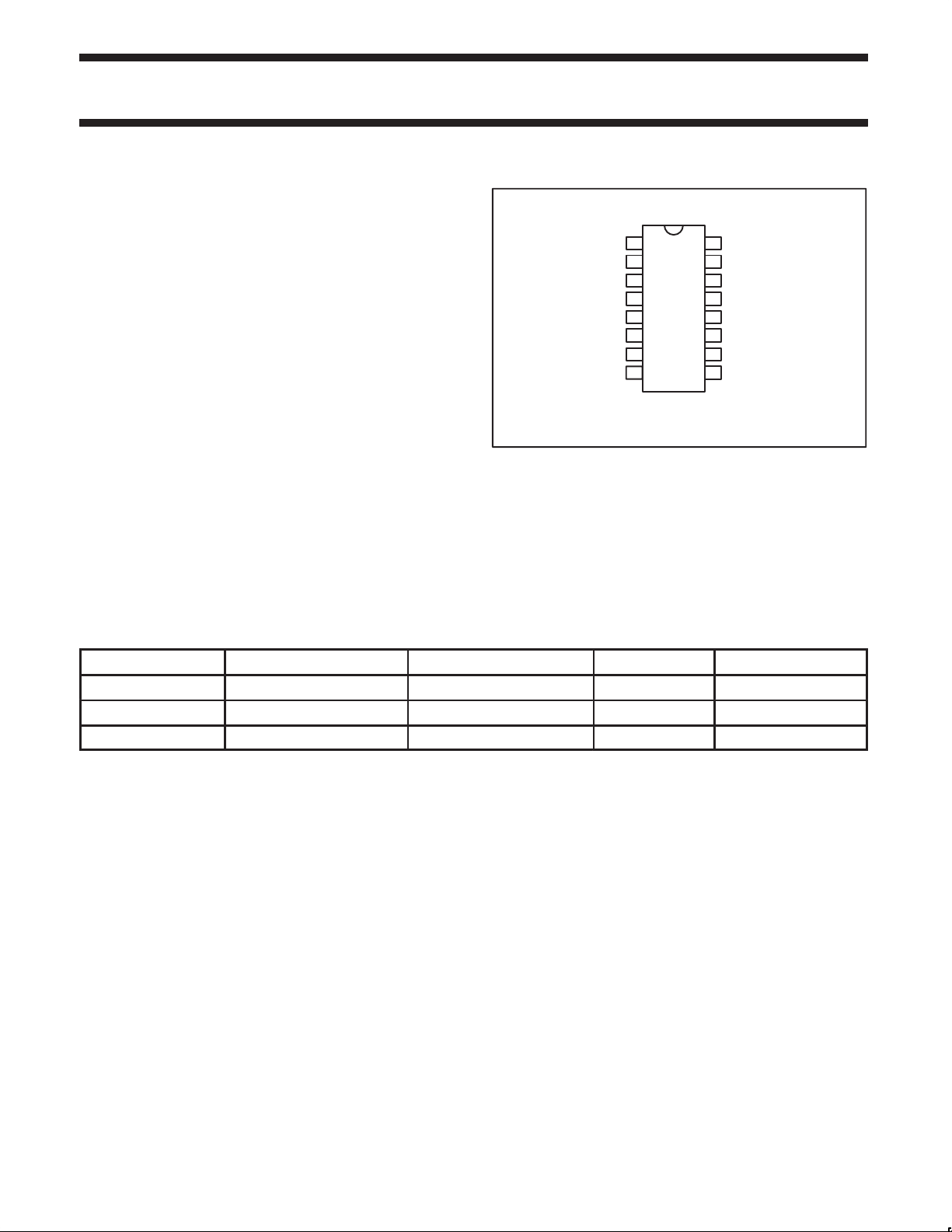
PIN CONFIGURATION
2
C SCL
1
I
2
2
C SDA
I
GND
3
4
5
6
7
8
OVERRIDE#
MUX_IN A
MUX_IN B
MUX_IN C
MUX_IN D
SW00216
V
16
CC
WP
15
NON_MUXED_OUT
14
MUX_SELECT
13
MUX_OUT A
12
11
MUX_OUT B
MUX_OUT C
10
MUX_OUT D
9
ORDERING INFORMATION
PACKAGES TEMPERATURE RANGE OUTSIDE NORTH AMERICA NORTH AMERICA DRAWING NUMBER
16-Pin Plastic SO 0°C to +70°C PCA8550D PCA8550D SOT109-1
16-Pin Plastic SSOP 0°C to +70°C PCA8550DB PCA8550DB SOT338-1
16-Pin Plastic TSSOP 0°C to +70°C PCA8550PW PCA8550PW DH SOT403-1
FUNCTIONAL DESCRIPTION
When the MUX_SELECT signal is logic 0, the multiplexer will select
the data from the non-volatile register to drive on the MUX_OUT
pins. When the MUX_SELECT signal is logic 1, the multiplexer will
select the MUX_IN lines to drive on the MUX_OUT pins. The
MUX_SELECT signal is also used to latch the NON_MUXED_OUT
signal which outputs data from the non-volatile register. The
NON_MUXED_OUT signal latch is transparent when MUX_SELECT
is in a logic 0 state, and will latch data when MUX_SELECT is in a
logic 1 state. When the active-LOW OVERRIDE# signal is set to
logic 0 and the MUX_SELECT signal is at a logic 0, all outputs will
be driven to logic 0. This information is summarized in Table 1.
The write protect (WP) input is used to control the ability to write the
contents of the 5-bit non-volatile register. If the WP signal is logic 0,
2
the I
C bus will be able to write the contents of the non-volatile
register. If the WP signal is logic 1, data will not be allowed to be
written into the non-volatile register.
The factory default for the contents of the non-volatile register are all
logic 0. These stored values can be read or written using the I
bus (described in the next section).
The OVERRIDE#, WP, MUX_IN, and MUX_SELECT signals have
internal pullup resistors. See the DC and AC Characteristics for
hysteresis and signal spike suppression figures.
2
C
1998 Sep 29 853-2015 20105
2
Philips Semiconductors Product specification
External in uts to multi lexer
2.5V multi lexed out ut
PCA85504-bit multiplexed/1-bit latched 5-bit I2C EEPROM
PIN DESCRIPTION
PIN
NUMBER
1 I2C SCL I2C bus clock
2 I2C SDA Bi-directional I2C bus data
3 OVERRIDE# Forces all outputs to logic 0
4 MUX_IN A
5 MUX_IN B
6 MUX_IN C
7 MUX_IN D
8 GND Common ground voltage rail
9 MUX_OUT D
10 MUX_OUT C
11 MUX_OUT B
12 MUX_OUT A
13 MUX_SELECT
14 NON_MUXED_OUT
15 WP
16 V
SYMBOL FUNCTION
p
p
Selects MUX_IN inputs or
register contents for
MUX_OUT outputs
TTL-level output from
non-volatile memory
Non-volatile register
write-protect
CC
Positive voltage rail
FUNCTION TABLE
Table 1. Function table
OVERRIDE
#
MUX_SELECT
0 0 All 0’ s All 0’s
0 1
p
1 0
1 1
NOTE
1. Latched NON_MIXED_OUT state will be the value present on
the NON_MUXED_OUT output at the time of the MUX_SELECT
p
input transitioned from a logic 0 to a logic 1 state.
MUX_OUT
OUTPUTS
MUX_IN
inputs
From non-
volatile
register
MUX_IN
inputs
NON_MUXED_OUT
OUTPUT
Latched
NON_MUXED_OUT
From non-volatile
register
From non-volatile
register
1
2
C Interface
I
Communicating with this device is initiated by sending a valid address on the I2C bus. The address format (see FIgure 1) is a fixed unique 7-bit
value followed by a 1-bit read/write value which determines the direction of the data transfer.
MSB LSB
10 0
11 1 0
R/W#
SW00218
Figure 1. I2C Address Byte
Following the address and acknowledge bit are 8 data bits which, depending on the read/write bit in the address, will read data from or write
data to the non-volatile register . Data will be written to the register if the read/write bit is logic 0 and the WP input is logic 0. Data will be read
from the register if the bit is logic 1. The three high-order bits (see FIgure 2) are logic 0. The next bit is data which is non-multiplexed. The low
four bits are the data which will be multiplexed. A write with any of the first three bits non-zero will be aborted.
NOTE:
1. To ensure data integrity, the non-volatile register must be internally write protected when V
component is dropped below normal operating levels.
to the I2C bus is powered down or VCC to the
CC
1998 Sep 29
3
Philips Semiconductors Product specification
PCA85504-bit multiplexed/1-bit latched 5-bit I2C EEPROM
MSB LSB
0
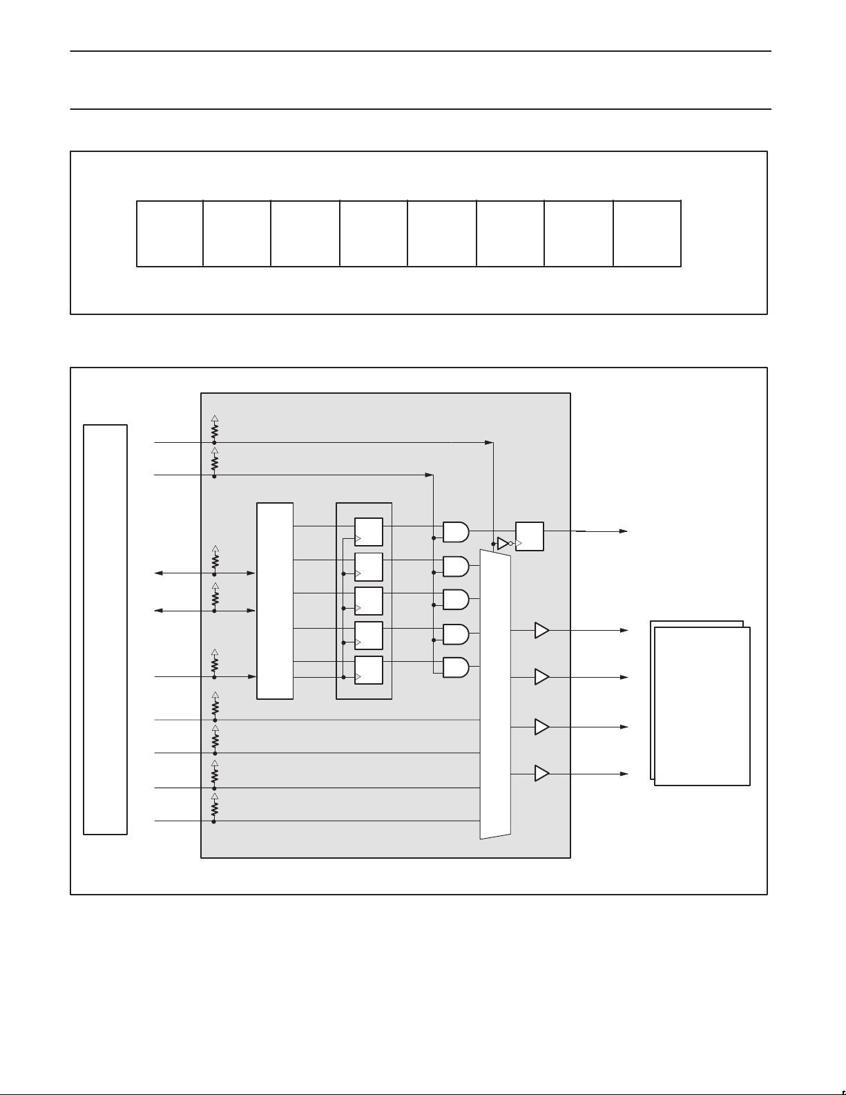
BLOCK DIAGRAM
CRESET#
13
MUX_SELECT
OVERRIDE#
3
= 16
V
CC3.3
GND = 8
SCL
1
2
I
C CLOCK
CHIP
SET
2
15
4
5
6
7
SDA
2
C DATA
I
WRITE
PROTECT
A20M#
MUX_IN A
IGNNE#
MUX_IN B
LINT0/INTR
MUX_IN C
LINT1/NMI
MUX_IN D
00
10–30k Ω
100–150k Ω
10–30k Ω
10–30k Ω
I C iNTERFACE LOGIC
2
OE#
NON-
MUXED
DATA
Figure 2. I2C Data Byte
5-BIT EEPROM
MUX
DATA D
MUX
DATA C
LATCH
NMO
0
3.3V
4-BIT 2-to-1 MULTIPLEXER
3.3V
3.3V
3.3V
1
MUX
DATA B
SELECT
NON_MUX_OUT
A20M#
2.5V
MUX_OUT A
/FSBM0
2.5V
IGNNE#
MUX_OUT B
/FSBM1
LINT0/INTR
2.5V
MUX_OUT C
/FSBM2
2.5V
LINT1/NMI
MUX_OUT D
/FSBM3
MUX
DATA A
SW00219
14
12
11
10
9
PENTIUM PRO/
PENTIUM II
PROCESSORS
1998 Sep 29
SW00347
4
 Loading...