

Philips PCA8516P, PCA8516T Datasheet

INTEGRATED CIRCUITS
DATA SH EET
PCA8516
Stand-alone OSD
Preliminary specification
File under Integrated Circuits, IC14
Philips Semiconductors
1995 Mar 30

Philips Semiconductors Preliminary specification
Stand-alone OSD PCA8516
CONTENTS
1 FEATURES
2 GENERAL DESCRIPTION
3 ORDERING INFORMATION
4 BLOCK DIAGRAM
5 PINNING INFORMATION
5.1 Pinning
5.2 Pin description
6 SERIAL I/O
6.1 I2C-bus serial interface
6.2 High-speed serial interface (HIO)
7 CHARACTER FONTS
7.1 Character font address map
7.2 Character font ROM
8 DISPLAY RAM ORGANIZATION
8.1 Description of display RAM codes
8.2 Loading character data into display RAM
8.3 Writing character data to display RAM
9 COMMANDS
9.1 Command 0
9.2 Command 1
9.3 Command 2
9.4 Command 3
9.5 Command 4
9.6 Command 5
9.7 Command 6
9.8 Command 7
9.9 Command 8
9.10 Command 9
9.11 Command A
9.12 Commands B, C and D
9.13 Command E
9.14 Command F
9.15 Command G
10 MISCELLANEOUS
10.1 Space and Carriage Return Codes in different
Background/Shadowing modes
10.2 Combination of character font cells
11 OSD CLOCK
12 OSD CLOCK SELECTION FOR DIFFERENT
TV STANDARDS
12.1 OSD frequency
12.2 Maximum number of characters per row
12.3 Maximum number of rows per frame
13 OUTPUT PORTS
13.1 Mask options
14 DEFAULT VALUES AFTER
POWER-ON-RESET
15 LIMITING VALUES
16 DC CHARACTERISTICS
17 AC CHARACTERISTICS
18 PACKAGE OUTLINES
19 SOLDERING
19.1 Introduction
19.2 DIP
19.3 SO
20 DEFINITIONS
21 LIFE SUPPORT APPLICATIONS
22 PURCHASE OF PHILIPS I2C COMPONENTS
1995 Mar 30 2
Philips Semiconductors Preliminary specification
Stand-alone OSD PCA8516
1 FEATURES
• Display RAM: 256 × 13 bits
• Display character fonts: 253 (fixed in ROM, mask
programmable)
• Starting position of the first character displayed:
64 vertical and 64 horizontal starting positions can be
selected by software
• Character size: 4 different character sizes on a
line-by-line basis (1 dot = 1H/1V; 2H/2V; 3H/3V and
4H/4V)
• Character matrix: 12 × 18 with no spacing between
characters and no rounding function
• Foreground colours: 16 combinations of Red, Green,
Blue and Intensity on character-by-character basis
• Background/shadowing modes: 4 modes available, No
background, Box shadowing, North-West shadowing
and Frame shadowing (raster blanking) on frame basis
• Background colours: 16 combinations of Red, Green,
Blue and Intensity on word-by-word basis. Available
when background mode is in either the Box shadowing,
North-West shadowing or Frame shadowing mode
• OSD oscillator: on-chip Phase-Locked Loop (PLL)
• Character blinking ratio: 1 : 1, 1 : 3 and 3 : 1
(programmable frequency of
f
) on character basis
VSYNC
⁄16,1⁄32,1⁄64or 1⁄
128
of
1
• Display format: flexible display format by using the
Carriage Return Code, maximum number of characters
per line is also flexible and depends upon the OSD clock
frequency
• Spacing between lines: 4 choices comprising 0, 4, 8 and
12 horizontal scan lines
• Display character RAM address auto-post-increment
when writing data
2
• Fast I
C-bus serial interface (400 kbaud) or High-speed
3-wire serial interface (1 Mbaud) for data/command
transfer
• ACM (Active Character Monitor) specifically for use in
camcorder applications on word basis; can also be used
as a 5th colour control with R, G, B and I signals
• Programmable active input polarity of HSYNC and
VSYNC
• Programmable output polarity of R, G, B, I and FB
• Supply voltage: 5 V ±10%
• Operating temperature: −20 to +70 °C
• Package: SDIP24 or SO24.
2 GENERAL DESCRIPTION
The PCA8516 is a member of the PCA85XX CMOS family
and is an on-screen character display generator controlled
by a microcontroller via the on-chip fast I
2
C-bus interface
or the on-chip High-speed 3-wire serial interface. It is
suitable for use in high-end TV or camrecorder
applications and has also been designed for use in
conventional mid-end TV with advanced graphic features.
3 ORDERING INFORMATION
PACKAGE
TYPE NUMBER
NAME DESCRIPTION VERSION
PCA8516P SDIP24 plastic shrink dual in-line package; 24 leads (400 mil) SOT234-1
PCA8516T SO24 plastic small outline package; 24 leads; body width 7.5 mm SOT137-1
1995 Mar 30 3
Philips Semiconductors Preliminary specification
Stand-alone OSD PCA8516
4 BLOCK DIAGRAM
ndbook, full pagewidth
P00
3
I/O
CONTROL
REGISTER
RAM
DISPLAY
CHARACTER
BUFFER
ADDRESS
SELECTOR
COUNTER
WRITE ADDRESS
P01
P04/ACM (VOB2)
PORT
BUFFERS
ROM
DISPLAY
VERTICAL
POSITION
COUNTER
REGISTER/
SS
AVDDAV
CONTROL
SIGNALS
ACM(VOB2)
DISPLAY CONTROL
AND OUTPUT STAGE
TESTING
CIRCUITRY
CRYSTAL
OSCILLATOR
MLC347
FB(VOB)
I(VOW3)
B(VOW2)
G(VOW1)
R(VOW0)
12
TEST2 TI00 to TI11
TEST1
Fig.1 Block diagram.
XTAL1(IN)
XTAL2(OUT)
POSITION
COUNTER
REGISTER/
HORIZONTAL
CONTROL
REGISTER/
CHARACTER SIZE
BUFFER
2
RECEIVER
I C SLAVE
RECEIVER OR
RESET
SCL/SCLK
HIGH-SPEED I/O
E
2
HIO/ I C
SDA/SIN
DATA SWITCHING
EXTERNAL/INTERNAL
SS
DD
V
V
1995 Mar 30 4
DECODER
INSTRUCTION
PLL
OSCILLATOR
C
CIRCUIT
INTERNAL
SYNCHRONOUS
HSYNC
CSYNC
VSYNC
HSYNC
SEPARATION
VSYNC
Philips Semiconductors Preliminary specification
Stand-alone OSD PCA8516
5 PINNING INFORMATION
5.1 Pinning
handbook, halfpage
P04/ACM (VOB2)
XTAL2 (OUT)
I (VOW3)
TEST2
TEST1
VSYNC
HSYNC
SDA/SIN
SCK/SCLK
XTAL1 (IN)
V
SS
1
2
3
4
C
5
6
PCA8516
7
8
9
10
11
12
MLC927
24
23
22
21
20
19
18
17
16
15
14
13
AV
DD
AV
SS
FB (VOB)
V
DD
B (VOW2)
P01
G (VOW1)
P00
R (VOW0)
2
HIO/I C
E
RESET
Fig.2 Pin configuration for SDIP24.
1995 Mar 30 5
Philips Semiconductors Preliminary specification
Stand-alone OSD PCA8516
5.2 Pin description Table 1 SDIP24 and SO24 packages
SYMBOL PIN I/O DESCRIPTION
I (VOW3) 1 O Character output signal for intensity control.
P04/ACM (VOB2) 2 O Port 04 output or Active Character Monitor output (VOB2).
TEST2 3 I Test mode selection; for normal operation TEST2 is connected to V
TEST1 4 I Test mode selection; for normal operation TEST1 is connected to V
C 5 I/O Capacitor connection for on-chip OSD PLL oscillator.
VSYNC 6 I Vertical synchronization input, active polarity programmable.
HSYNC 7 I Horizontal synchronization input, active polarity programmable.
SDA/SIN 8 I/O Data line of the I
2
C-bus interface or the data line for the High-speed
serial interface.
SCL/SCLK 9 I/O Clock line of the I
2
C-bus interface or the clock line for the High-speed
serial interface.
XTAL1 (IN) 10 I System clock input.
XTAL2 (OUT) 11 O System clock output.
V
SS
12 I Ground, digital.
RESET 13 I Master Reset input (active LOW).
E 14 I Chip enable (active HIGH) for the High-speed serial interface. When the
2
C-bus interface is selected this pin should be connected to VSS.
I
HIO/I2C 15 I Serial interface selection. When this pin is LOW the High-speed serial
interface is selected; when this pin is HIGH the I2C-bus interface is
selected.
R (VOW0) 16 O Character output signal: VOW0 for Red.
P00 17 I/O General purpose I/O Port 00.
G (VOW1) 18 O Character output signal: VOW1 for Green.
P01 19 I/O General purpose I/O Port 01.
B (VOW2) 20 O Character output signal: VOW2 for Blue.
V
DD
21 I Power supply, digital.
FB (VOB) 22 O Fast Blanking output (VOB).
AV
AV
SS
DD
23 I Ground, analog.
24 I Power supply, analog.
SS
SS
.
.
1995 Mar 30 6

Philips Semiconductors Preliminary specification
Stand-alone OSD PCA8516
6 SERIAL I/O
The PCA8516 has two means by which it can
communicate with a microcontroller: a fast I2C-bus serial
interface and a High-speed serial interface. Selection of
either interface is achieved via pin 15, HIO/I2C. When
HIO/I2C is LOW, the HIO serial interface is selected. When
HIO/I2C is HIGH, the I2C-bus serial interface is selected.
The PCA8516 is programmed by a series of commands
sent via one of these interfaces. There are 16 commands;
each command selecting different functions of the
PCA8516. The 16 commands are described in detail in
Chapter 9.
2
6.1 I
C-bus serial interface
The I2C-bus serial interface is selected by driving pin 15
(HIO/I2C) HIGH. Data transmission conforms to the fast
I2C-bus protocol; the maximum transmission rate being
400 kHz. The PCA8516 operates in the slave receiver
mode and therefore in normal operation is ‘write only’ from
the master device.
The format of the data streams sent via the I2C-bus
interface is shown in Fig.3. The first data byte is the slave
address 1011 101Xb. The last bit of the slave address is
always a logic 0, except in the Test mode when it could be
a logic 1. Subsequent data bytes contain the commands
for control of the device. Upon the successful reception of
a complete data byte by the shift register, an Acknowledge
bit is sent. A STOP condition terminates the data transfer
operation.
The I2C-bus interface is reset to its initial state (waiting for
a slave address call) by the following conditions:
• After a master reset
2
• After a bus error has been detected on the I
C-bus
interface.
Under both these conditions the data held in the shift
register is abandoned.
6.1.1 M
AXIMUM SPEED OF THE I
2
C-BUS
The maximum I2C-bus transmission rate that the
PCE8515 can receive is 400 kHz. However, if the data
byte being transmitted is for display RAM then internal
synchronization of the write operation from the shift
register to the display RAM location is necessary. This will
reduce the maximum transmission speed.
The synchronization process is carried out by on-chip
hardware and takes place during the HSYNC retrace
period when VSYNC is inactive. The I
2
C-bus clock is
pulled LOW if a complete display RAM data byte is
received before HSYNC becomes active. The I2C-bus
clock will be released when HSYNC becomes active and
then the contents of the shift register will be written into the
display RAM location.
6.2 High-speed serial interface (HIO)
The High-speed serial interface is selected when pin 15
(
HIO/I2C) is pulled LOW. The High-speed serial interface
has a 3-wire communication protocol; the maximum
transmission rate being 1 MHz. The interface protocol is
illustrated in Fig.4 and described below.
1. Pin 14 (E) the chip enable pin is driven HIGH. This
LOW-to-HIGH transition clears the shift register and
resets the serial input circuit.
2. On the first HIGH-to-LOW transition of SCLK after the
interface has been enabled, the first data bit (D0) must
be present at the SIN pin.
3. On the following LOW-to-HIGH transition of SCLK, the
first data bit (D0) will be latched into the shift register.
4. On the next HIGH-to-LOW transition of SCLK the
second data bit (D1) must be present at the SIN pin.
Data bit (D1) will be latched into the shift register on
the following LOW-to-HIGH transition of SCLK.
5. The operation specified in step 4 above is repeated
another 6 times, thus loading the shift register with a
complete data byte. This data byte is then transferred
to the command interpreter which takes the
appropriate action.
6. Providing the chip enable signal remains HIGH, a
2nd data byte can be transferred. The 1st data bit of
the next data transfer takes place on the falling edge
of the SCLK signal.
The following points should be noted:
• If the chip enable signal is pulled LOW at any time the
shift operation in progress is stopped and the HIO slave
receiver is disabled
• The rising edge of the chip enable signal resets the HIO
slave receiver.
1995 Mar 30 7
Philips Semiconductors Preliminary specification
Stand-alone OSD PCA8516
2
handbook, full pagewidth
I C-bus
bit stream
S Slave address Ack Ack
1st data byte
Command
Register data
LSBMSB
870870
W
O
0 1 1 1 1 0 0
2nd data byte
bit 7
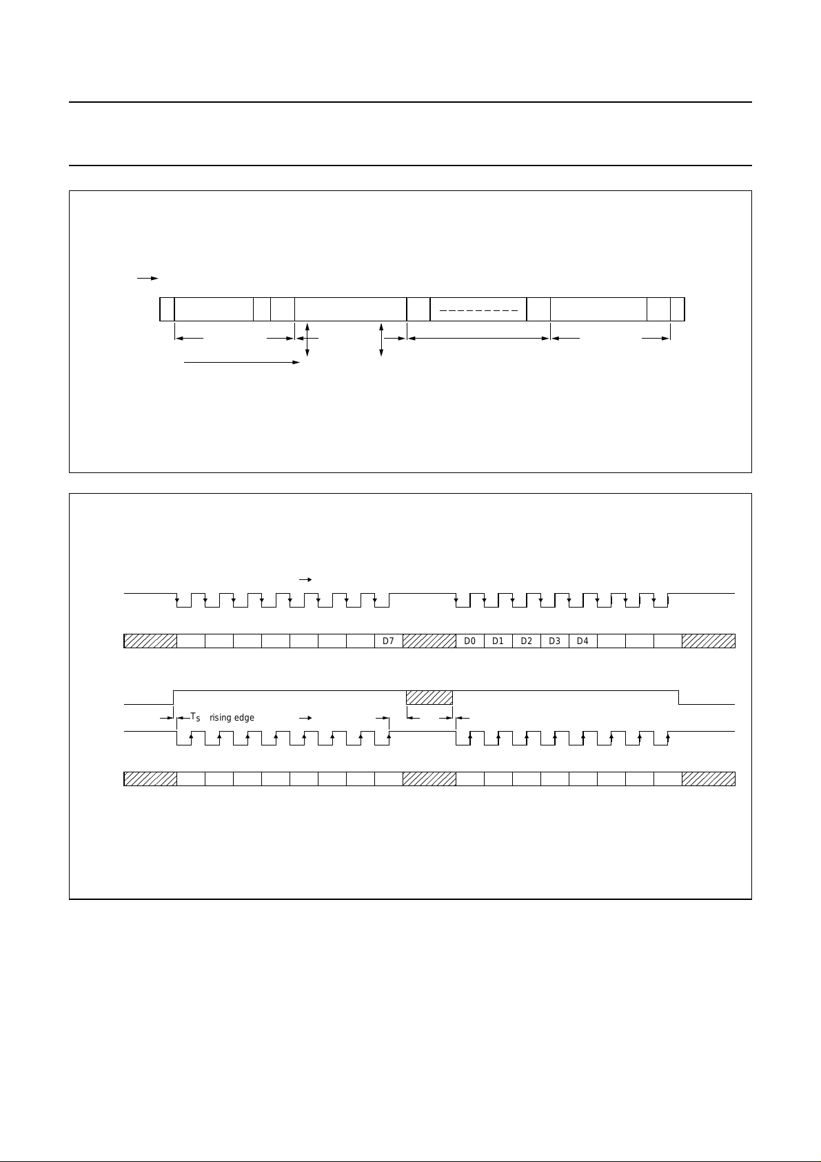
Fig.3 I2C-bus write timing diagram - data stream.
BS
bit 0
Ack
870
nth data byte
807
Ack
P
MRA818
handbook, full pagewidth
SCLK
D
(from HIO master and
connected to SIN pin of
HIO slave)
E
SCLK
(1) Ts≥ 1µs; Th≥ 1 µs.
falling edge of SCLK D changes
D0 D1 D2 D3 D4 D5 D6 D7 D0 D1 D2 D3 D4 D5 D6 D7OUT
T
rising edge of SCLK SIN sampled
s
D0 D1 D2 D3 D4 D5 D6 D7 D0 D1 D2 D3 D4 D5 D6 D7SIN
OUT
T
h
T
s
Fig.4 High-speed I/O format.
MLB395 - 1
1995 Mar 30 8
Philips Semiconductors Preliminary specification
Stand-alone OSD PCA8516
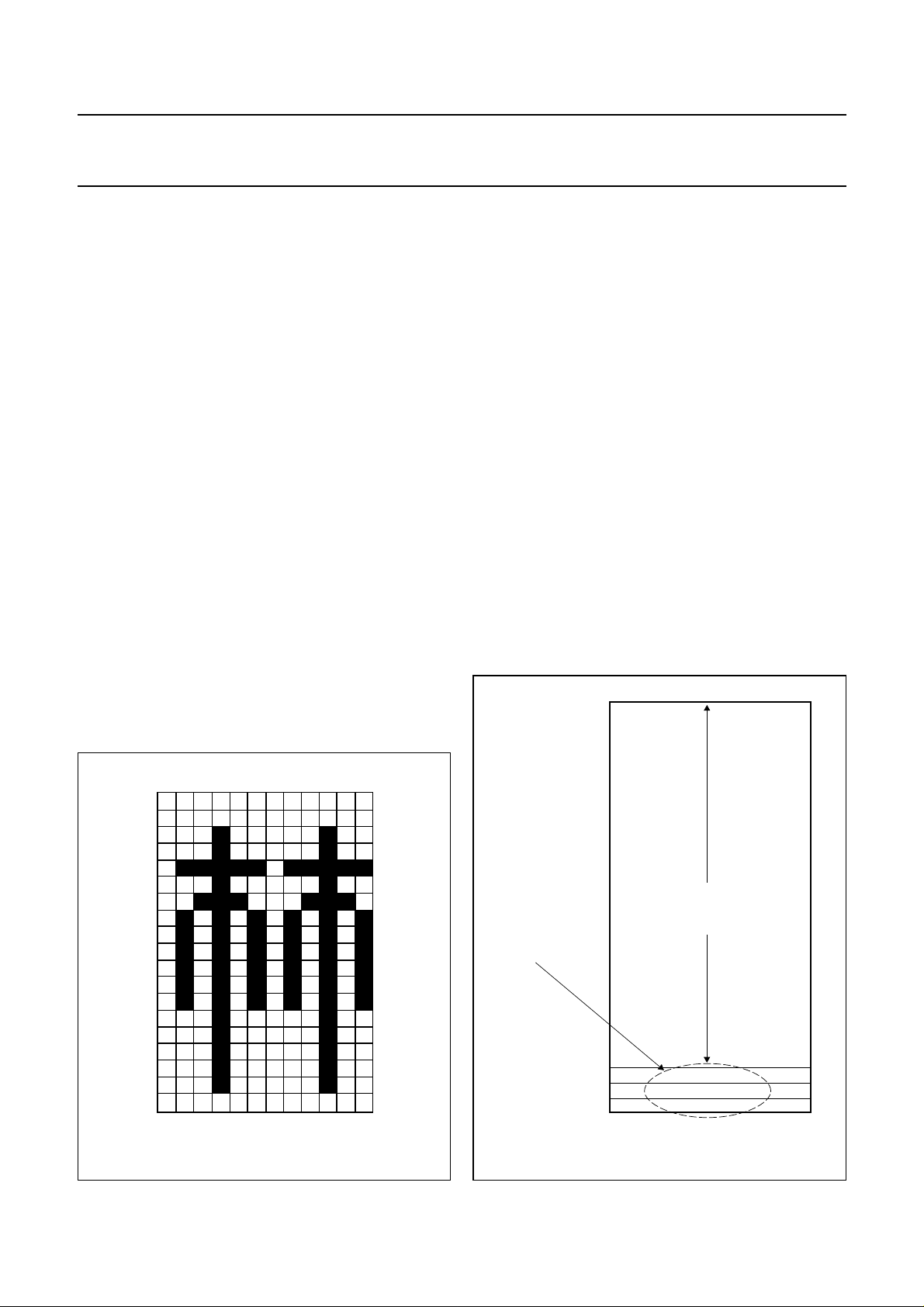
7 CHARACTER FONTS
256 character fonts may be held in ROM; 253 customer
selected fonts and three reserved character font codes.
Customer selected fonts are mask programmable. Each
character font is stored in a 12 × 19 dot matrix, as shown
in Fig.5. Elements in Rows 1 to 18 can be selected as
visible dots on the screen; Row 0 is used only for the
combination of two characters in a vertical direction, when
the North-West shadowing mode is selected (see
Sections 9.9 and 10.2). Extremely high resolution can be
achieved by having no spacing between characters on the
same line and by programming the inter-line spacing to
zero. The 12 × 18 dot matrix is suitable for the display of
semigraphic patterns, Kanji, Hiragana, Katagana or even
Chinese characters.
7.1 Character font address map
Figure 6 shows the character font address map in ROM
and RAM. Addresses FFH and FEH hold the reserved
codes for space and carriage return functions respectively;
address FDH is reserved for testing purposes and
addresses (00H to FCH) contain the character font codes.
7.2 Character font ROM
The file format to submit to Philips for customized
character sets is also shown in Fig.7. The following points
should be noted:
1. Row 0 of each font is reserved for vertical combination
of two fonts.
2. When two font cells are combined in a vertical
direction Row 0 of the lower font must contain the
same bit pattern as held in Row 18 of the character
above it.
3. Binary 1 denotes visual dots; binary 0 denotes a blank
space.
4. ROM1 and ROM2 data files are in INTEL hex format
on a byte basis. Each byte is structured High nibble
followed by Low nibble.
5. The remaining unused 16 bytes (one character font) in
ROM1/ROM2 must be filled with FFH.
6. CS denotes Checksum.
A software package (OSDGEM) that assists in the design
of character fonts on-screen and that also automatically
generates the bit pattern HEX files, is available on request.
The package is run under the MS-DOS environment for
IBM compatible PCs.
ROM is divided into two parts: ROM1 and ROM2. The
organization of the bit patterns stored in ROM1 and ROM2
is shown in Fig.7.
01234567891011
0
1
2
3
4
5
6
7
8
9
10
11
12
13
14
15
16
17
18
MLC350
reserved code
252 (FCH)
253 (FDH)
254 (FEH)
255 (FFH)
0
Mask Programmable Font
Test code
Carriage return code
Space code
MLB344
Fig.5 Character dot matrix organization.
1995 Mar 30 9
Fig.6 ROM address map.
Philips Semiconductors Preliminary specification
Stand-alone OSD PCA8516
Column
MSB
1110987 6543210
0
1
2
3
4
5
6
Row
7
8
9
10
11
12
13
14
15
16
17
18
ROM1
: 1 0 0 0 0 0 0 0 00 00 22 FC 03 22 20 F2 3F 01 20 55 0C 00 03
: 1 0 0 0 1 0 0 0 < - - - DATA FOR FONT 2 - - - >
: 1 0 0 0 2 0 0 0 < - - - DATA FOR FONT 3 - - - >
byte #
0 1 2 3 4 5 6 7 8 9 A B C D E F
__ __ __ __ __ __ __ __ __ __ __ __ __ __ __
LSB
0 0 0
3 F C
2 2 0
2 2 0
3 F C
2 2 0
2 2 0
3 F C
2 2 0
2 2 0
3 F F
0 0 1
0 0 1
5 5 3
5 5 2
0 0 6
0 0 C
0 5 8
0 3 0
ROM1
ROM2
ROM1
ROM2
ROM1
ROM2
ROM1
ROM2
ROM1
ROM2
ROM1
ROM2
ROM1
ROM2
ROM1
ROM2
ROM1
ROM2
ROM1
ROM2
: 1 0 0 0 0 0 0 0 FC 03 22 20 C2 3F 20 12 00 53 65 00 58
: 1 0 0 0 1 0 0 0 < - - - DATA FOR FONT 2 - - - >
: 1 0 0 0 2 0 0 0 < - - - DATA FOR FONT 3 - - - >
ROM1 ROM2
0 0 0
2 2 0
3 F C
2 2 0
2 2 0
3 F F
0 0 1
5 5 2
0 0 C
0 3 0
F F C S
F F C S
F F C S
F 0 FF FF C S
F X FF FF C S
F X FF FF C S
3 F C
2 2 0
2 2 0
3 F C
2 2 0
0 0 1
5 5 3
0 0 6
0 5 8
MLB345
Fig.7 Character font pattern stored in ROM1 and ROM2.
1995 Mar 30 10
Philips Semiconductors Preliminary specification
Stand-alone OSD PCA8516
8 DISPLAY RAM ORGANIZATION
The display RAM is organized as 256 × 13 bits. The
general format of each RAM location is as follows.
Bits <12-5> hold character data and allow a choice from
253 customer designed character fonts to be selected or
one of three reserved codes. Bits <4-0> contain the
attributes of the character font, for example colour,
character size etc.
8.1 Description of display RAM codes
There are four data formats for display RAM code:
1. Character Font Code
2. Test Code
3. Carriage Return Code
4. Space Code.
The above data formats allow great flexibility in the
creation of On Screen Displays; see Fig.8.
8.1.1 C
HARACTER FONT CODE
If bits <12-5> are in the range (00H to FCH), then this is a
Character Font Code. 1 of 253 customer designed
character fonts can be selected. Bits <4-1> determine the
colour of the character, a choice of 16 colours being
available. Bit <0> determines whether the character blinks
or not. The format of the Character Font Code is shown in
Table 2.
8.1.2 T
EST CODE
8.1.3 C
ARRIAGE RETURN CODE
If bits <12-5> hold FEH, then this is the Carriage Return
Code. A transparent pattern will be displayed on the
screen and the next character will be displayed at the
beginning of the next line. Bits <4-3> select the size of the
characters to be displayed on the next line. Bits <2-1>
determine the spacing between lines of displayed
characters. Bit <0> is the End of Display bit and indicates
the end of display of the current screen before exhaustion
of display RAM (i.e. before the 256th RAM location). The
format of the Carriage Return Code is shown in Table 3.
8.1.4 S
PACE CODE
If bits <12-5> hold FFH, then this is the Space Code.
A transparent pattern, equal to one character width, will be
displayed on the screen. A mask programmable option is
available that allows the space character to be transparent
or to have a programmable background colour;
see Section 13.1. Bits <4-1> determine the background
colour of the characters that follow the Space Code in both
the Box shadowing and North-West shadowing modes.
Bit <0> is the Active Character Monitor (ACM)
enable/disable bit. The ACM signal is specifically for use in
camrecorder applications where part of the display is to be
recorded on tape and displayed on the screen, whilst the
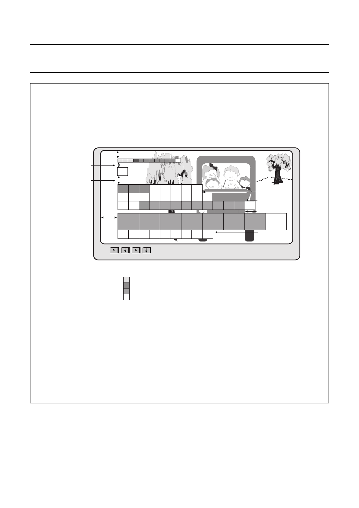
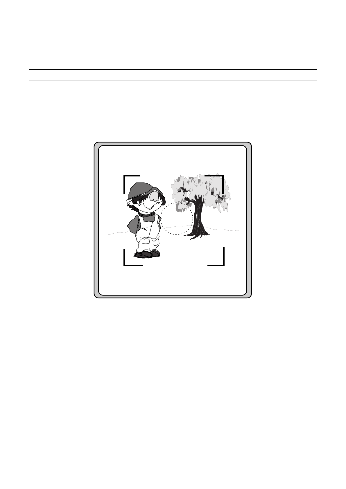
remaining part is for display only. Figure 9 shows a typical
ACM application. During the back-tracing period R, G, B, I,
FB and ACM are inactive. The format of the Space Code
is shown in Table 4.
If bits <12-5> hold FDH, then this is a special code
reserved for testing purposes only.
Table 2 Format of Character Font Code
121110987654321 0
C7 C6 C5 C4 C3 C2 C1 C0 T4 T3 T2 T1 T0
Character Font Code (00H - FCH) Foreground colour Blink
Table 3 Format of Carriage Return Code
1211109876543210
C7 C6 C5 C4 C3 C2 C1 C0 T4 T3 T2 T1 T1
Carriage Return Code (FEH) Character size Line Spacing End
Table 4 Format of Space Code
1211109876543210
C7 C6 C5 C4 C3 C2 C1 C0 T4 T3 T2 T1 T0
Space Code (FFH) Background colour ACM
1995 Mar 30 11
Philips Semiconductors Preliminary specification
Stand-alone OSD PCA8516
handbook, full pagewidth
line spacing 1 = 4H
line spacing 2 = 8H
Vstart
HI ! TH
CR
T H E N E W
IS I
SP SP CR
SP
F U N C I O NT
I N P C A 8 5 1 0
Hstart
SP
Volume
Four different background colours (in box shadowing mode):
SP
ST ANDAL
E L C O M EW
Channel
BLACK
RED
GREEN
BLUE
S
CR
CR
CR
line spacing 3 = 0H
line spacing 4 = 0H
CR
line spacing 4 = 4H
line spacing 6 = 0H
CR
MRA832
Fig.8 Example of On Screen Display.
1995 Mar 30 12
Philips Semiconductors Preliminary specification
Stand-alone OSD PCA8516
handbook, full pagewidth
Battery Status : OK
Shutter speed : 500
Focal Length : 28 mm
PHILIPS
Made by MOS IC TAIWAN, PHILIPS
In this example, all the characters are displayed on the viewfinder.
As only the data 'Date : July 15, 1994' is to be recorded onto the tape,
only these characters' ACM attribute bit is set to a logic 1.
Date : July 15, 1994
MRA831
Fig.9 Example of ACM signal for use in camrecorder applications.
1995 Mar 30 13
Philips Semiconductors Preliminary specification
Stand-alone OSD PCA8516
8.2 Loading character data into display RAM
Three registers are used to address and load data into the
display RAM. These registers are described below.
8.2.1 DCR A
DDRESS REGISTER (DCRAR)
Table 5 DCR Address Register
76543210
A7 A6 A5 A4 A3 A2 A1 A0
This register holds the address of the location in display
RAM into which data is to be written. Command 3 loads
the High nibble of the address into this register;
Command 4 loads the Low nibble of the address.
8.2.2 DCR A
TTRIBUTE REGISTER (DCRTR)
Table 6 DCR Attribute Register
76543210
−−−T4 T3 T2 T1 T0
The Attribute Register is loaded with character font
attribute data using Command 2. The data will be loaded
into bits <4-0> of the location in RAM addressed by the
contents of DCRAR. Bits 7 to 5 are not used and are
reserved.
8.3 Writing character data to display RAM
The procedure for writing character data to the display
RAM is as follows:
1. Select the start address in display RAM. The start
address can take any value between 0 and 255.
Command 3 is used to load the High nibble of the start
address. Command 4 is used to load the Low nibble of
the start address. The start address is stored in
DCRAR.
2. Load the character attributes into DCRTR using
Command 2. The actual attribute selected is
dependent upon whether the Character Font Code,
Carriage Return Code or Space Code has been
selected by Command 1 (see Section 8.1).
If the attributes of a series of displayed characters are
the same, the contents of this register need not be
updated.
3. Load the Character Font data into DCTCR using
Command 1 or Command 5. Either of these
commands signal that a complete command byte is
available and the data held in registers DCRTR and
DCRCR is loaded into the RAM location pointed to by
the address stored in DCRAR. The address held in
DCRAR is then incremented by ‘1’ pointing to the next
RAM location in anticipation of the next operation.
A description of all the Commands is given in Chapter 9.
8.2.3 DCR C
HARACTER REGISTER (DCRCR)
Table 7 DCR Character Register
76543210
C7 C6 C5 C4 C3 C2 C1 C0
This register holds the character font data loaded by
Command 1. The data will be loaded into bits <12-5> of
the location in RAM addressed by the contents of DCRAR.
1995 Mar 30 14
Philips Semiconductors Preliminary specification
Stand-alone OSD PCA8516
9 COMMANDS
The PCA8516 is programmed by a series of commands sent by a microcontroller via the I2C-bus interface or the
High-speed serial interface. 17 commands (Commands 0 to G) are available for selecting the various functions of the
PCA8516. A command overview is shown in Table 8; full descriptions of each command are given in Sections 9.1 to 9.15.
Table 8 Command overview (note 1)
COMMAND BS1 BS0 7 6543210
0 Command Bank selection X X 0 11110BS1BS0
1 Character font selection - Bank 1 0 0 1 C6 C5 C4 C3 C2 C1 C0
2 Character attributes X 0 0 0 0 T4 T3 T2 T1 T0
3 Display Character Address High 0 0 0 0 1 0 A7 A6 A5 A4
4 Display Character Address Low 0 0 0 0 1 1 A3 A2 A1 A0
5 Character font selection - Bank 2 1 0 1 C6 C5 C4 C3 C2 C1 C0
6 OSD PLL oscillator divisor 0 1 0 0 D5 D4 D3 D2 D1 D0
7 Scan mode, polarity of FB, ACM, R,
G, B and I; OSD enable/disable
8 Polarity of HSYNC and VSYNC,
Display mode
9 Blinking frequency, blinking
frequency active ratio
A I/O port selection 0 1 0 1110A/P00
B Vertical start position High 0 1 1 0 0 1 V5 V4 V3 V2
C Vertical start position Low/
Horizontal start position High
D Horizontal start position Low 0 1 1 0 1 1 H3 H2 H1 H0
E Write to ports P00, P01 and P04 0 1 1 1 X P04 X X P01 P00
F Background colour in Frame
shadowing mode
G Enable/disable OSD horizontal
stabilization circuit (Regen H),
selection of Half-tone background
mode and character size of first line
0 1 0 1 0 0 M1 M0 Bp EN
0 1 0 1 0 1 Hp Vp S1 S0
0 1 0 1 1 0 BF1 BF0 BR1 BR0
0 1 1 0 1 0 V1 V0 H5 H4
0 00100RGBI
0 0 0 1 0 1 HM3 HT2 FS1 FS0
Note
1. ‘X’ denotes don’t care state.
1995 Mar 30 15
Philips Semiconductors Preliminary specification
Stand-alone OSD PCA8516
9.1 Command 0 Table 9 Command 0 format
76543210
0 1 1 1 1 0 BS1 BS0
Command 0 is used to select the Command Bank. Bits
BS1 and BS0 are the two flags that indicate the current
Command Bank being executed. During a master reset
these two bits are cleared (BS1 = 0, BS0 = 0). Each
command has its own associated Command Bank, this is
shown in Table 8.
9.2 Command 1 Table 10 Command 1 format
BS1BS076543210
0 0 1 C6C5C4C3C2C1C0
Command 1 is used to load character data into the DCR
Character Register. The data will specify either a
Character Font Code, the Test Code, the Carriage Return
Code or the Space Code. These codes are explained in
detail in Section 8.1.
9.3 Command 2 Table 11 Command 2 format
9.3.1 CHARACTER FONT CODE ATTRIBUTES
Command 2 when used in conjunction with a Character
Font Code (80H to FCH) will select 1 of 16 foreground
colours and enables/disables the Blinking function.
Table 12 Selection of Foreground colour
T4 T3 T2 T1
RGB I
0000
0001
0010
0011
0100
0101
0110
0111
1000
1001
1010
1011
1100
1101
1110
1111
BS1BS076543210
X 0 0 0 0 T4T3T2T1T0
This command writes character attribute data into the DCR
Attribute Register. The actual character attribute is
dependent upon the code selected by Command 1. See
the data formats shown in Tables 2, 3 and 4.
1995 Mar 30 16
Table 13 Selection of Blinking function
T0 BLINKING
0 OFF
1ON
Philips Semiconductors Preliminary specification
Stand-alone OSD PCA8516
9.3.2 CARRIAGE RETURN CODE ATTRIBUTES
Command 2 when used in conjunction with the Carriage
Return Code (FEH) determines the size of characters to be
displayed on the next line, sets the spacing between lines
of characters and enables/disables the display.
The character size is also a function of the TV scanning
standard being used and f
Chapter 12.
Table 14 Selection of character size
T4 T3 CHARACTER DOT SIZE
0 0 1H/1V (the default size)
0 1 2H/2V
1 0 3H/3V
1 1 4H/4V
Table 15 Selection of line spacing
T2 T1
0 0 0H line
0 1 4H line
1 0 8H line
1 1 12H line
Table 16 End of display control
T0 DISPLAY CONTROL
0 Continue to display next character. This
is also the default setting.
1 End of display.
; this is explained in
OSD
LINE SPACING
(BETWEEN TWO ROWS)
Table 17 Selection of Background colour
T4 T3 T2 T1
RGB I
0000
0001
0010
0011
0100
0101
0110
0111
1000
1001
1010
1011
1100
1101
1110
1111
Table 18 ACM control
T0 ACM PIN
0 The ACM pin is inactive; this is also the
default setting.
1 The ACM function is active for all
characters displayed following this
Space Code.
9.3.3 S
Command 2 when used in conjunction with the Space
Code (FFH) selects the background colour of characters in
Box shadowing or North-West shadowing modes and also
controls the Active Character Monitor pin. The ACM pin will
remain active until a Space Code is received that resets
the ACM bit to logic 0. The ACM timing diagram is shown
in Fig.10.
1995 Mar 30 17
PACE CODE ATTRIBUTES
Philips Semiconductors Preliminary specification
Stand-alone OSD PCA8516
handbook, full pagewidth
FB
ACM
0
18
R
G
B
I
'S' : Red
'I' : Green
'Z' : Green + Blue + Intensity
'E' : Blue + Intensity
1st SP code : ACM = on
2nd SP code: ACM = off
SP code SP code
MRA830 - 1
Fig.10 R, G, B, I - ACM timing.
1995 Mar 30 18
Philips Semiconductors Preliminary specification
Stand-alone OSD PCA8516
9.4 Command 3 Table 19 Command 3 format
BS1BS076543210
0 0 0 0 1 1 A7 A6 A5 A4
Command 3 loads the DCR Address Register with the
4 MSBs of the RAM address to which data will be written.
9.5 Command 4 Table 20 Command 4 format
BS1BS076543210
0 0 0 0 1 1 A3 A2 A1 A0
Command 4 loads the DCR Address Register with the
4 LSBs of the RAM address to which data will be written.
9.6 Command 5 Table 21 Command 5 format
BS1BS076543210
1 0 1 C6C5C4C3C2C1C0
Command 5 is used to load character data into the DCR
Character Register. The data will specify either a
Character Font Code, the Test Code, the Carriage Return
Code or the Space Code. These codes are explained in
detail in Section 8.1.
9.7 Command 6 Table 22 Command 6 format
9.8 Command 7 Table 23 Command 7 format
BS1BS076543210
0 1 0 1 0 0 M1 M0 Bp EN
This command loads Control Register 1 with data that
selects the scanning mode, the output polarity of signals
FB, ACM, R, G, B and I, and also enables/disables the
OSD clock.
With reference to the scanning modes: 1V/2V is the
conventional NTSC or PAL scanning mode; 1V/2H is the
Line Progress Scan used for the IDTV in NTSC and 2V/2H
is for the PAL system and is known as 50 Hz to 100 Hz
scan conversion.
Table 24 Selection of Scanning Mode
M1 M0 SCAN MODE
0 0 1V/1H; NTSC 525LPF/60 Hz or
PAL 625LPF/50 Hz; see Fig.11. This is
the default setting.
0 1 reserved
1 0 1V/2H; NTSC 1050LPF/60 Hz; see
Fig.11.
1 1 2V/2H; PAL 1250LPF/100 Hz; see
Fig.12.
Table 25 Selection of output polarity (see Fig.13)
Bp OUTPUT POLARITY (FB, ACM, R, G, B, I)
0 active LOW
1 active HIGH (the default setting)
BS1BS076543210
0 1 0 0 D5 D4 D3 D2 D1 D0
Command 6 loads the programmable 6-bit counter of the
OSD clock oscillator. The output frequency (f
function of the decimal value of the 6-bits loaded in by
Command 6; see Chapter 11.
1995 Mar 30 19
OSD
) is a
Table 26 OSD clock control
EN OSD CLOCK
0 disabled (the default setting)
1 enabled
Philips Semiconductors Preliminary specification
Stand-alone OSD PCA8516
handbook, full pagewidth
VSYNC
HSYNC
VSYNC
HSYNC
f = 15734 Hz
HSYNC
f = 31468 Hz
HSYNC
f = 60 Hz
VSYNC
262.5 lines 262.5 lines
(a) Conventional NTSC 1V/1H
f = 60 Hz
VSYNC
525 lines 525 lines
(b) NTSC 1V/2H
f = 60 Hz
VSYNC
f = 60 Hz
VSYNC
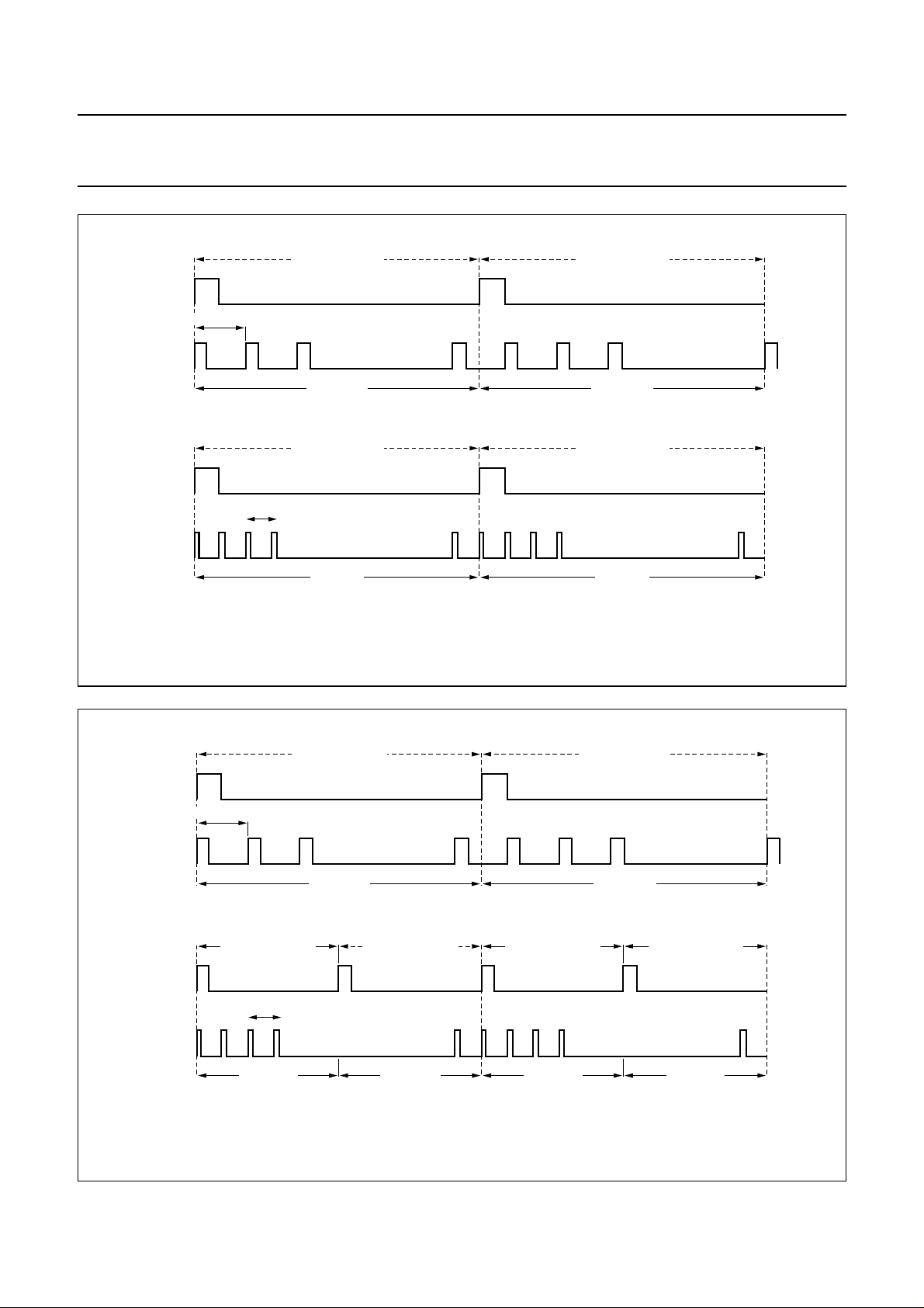
Fig.11 NTSC scan formats.
MRA834
handbook, full pagewidth
VSYNC
f = 15625 Hz
HSYNC
VSYNC
HSYNC
HSYNC
f = 31250 Hz
f = 50 Hz
f = 100 Hz
VSYNC
HSYNC
VSYNC
312.5 lines
(a) Conventional PAL 1V/1H
f = 100 Hz
VSYNC
(b) PAL 2V/2H
f = 100 Hz
VSYNC
Fig.12 PAL scan formats.
f = 50 Hz
VSYNC
312.5 lines
f = 100 Hz
VSYNC
312.5 lines312.5 lines312.5 lines312.5 lines
MRA835
1995 Mar 30 20
 Loading...