

Philips pca84c64 DATASHEETS

INTEGRATED CIRCUITS
DATA SH EET
PCA84C646; PCA84C846
Microcontrollers for TV tuning
control and OSD applications
Preliminary specification
Supersedes data of June 1994
File under Integrated Circuits, IC14
1995 Jun 15

Philips Semiconductors Preliminary specification
Microcontrollers for TV tuning
control and OSD applications
CONTENTS
1 FEATURES
1.1 PCF84CXXXA kernel
1.2 VST and OSD derivative
2 GENERAL DESCRIPTION
3 ORDERING INFORMATION
4 BLOCK DIAGRAM
5 PINNING INFORMATION
5.1 Pinning
5.2 Pin description
6 RESET
6.1 Reset trip level
6.2 Reset status
7 ANALOG CONTROL
7.1 6 and 7-bit PWM outputs (PWM00 to PWM07)
7.2 VST control 14-bit PWM DAC
8 AFC INPUT
9 OSD (ON SCREEN DISPLAY) FUNCTION
9.1 Features
9.2 Horizontal display position control
9.3 Vertical display position control
9.4 Clock generator
10 DISPLAY RAM ORGANIZATION
10.1 Description of display RAM codes
10.2 Loading character data into display RAM
10.3 Writing character data to display RAM
10.4 Default value of the display character
11 CHARACTER ROM
11.1 Character ROM organization
PCA84C646; PCA84C846
12 OSD CONTROL REGISTERS
12.1 Derivative Register 22 (CON1)
12.2 Derivative Register 23 (CON2)
12.3 Derivative Register 33 (CON3)
12.4 Derivative Register 34 (CON4)
12.5 Derivative Register 35 (VPOS)
12.6 Derivative Register 36 (HPOS)
12.7 Derivative Register 37 (BCC)
13 COMBINATION OF TWO OR MORE FONT
CELLS TO FORM A NEW FONT
14 OSD CLOCK IN DIFFERENT TV
STANDARDS
14.1 Maximum number of characters per row
14.2 Maximum number of rows per frame
15 T3: 8-BIT COUNTER
16 I2C-BUS MASTER SLAVE TRANSCEIVER
17 DERIVATIVE REGISTERS
18 INPUT/OUTPUT
19 OPTION LISTS
20 LIMITING VALUES
21 DC CHARACTERISTICS
22 AC CHARACTERISTICS
23 AFC CHARACTERISTICS
24 PACKAGE OUTLINE
25 SOLDERING
26 DEFINITIONS
27 LIFE SUPPORT APPLICATIONS
28 PURCHASE OF PHILIPS I2C COMPONENTS
1995 Jun 15 2

Philips Semiconductors Preliminary specification
Microcontrollers for TV tuning
control and OSD applications
1 FEATURES
1.1 PCF84CXXXA kernel
• 8-bit CPU, ROM, RAM, I/O and derivative logic in one
package
• Over 80 instructions
• All instructions of 1 or 2 cycles
• Quasi-bidirectional standard I/O port lines (P0, P1)
• Configuration of I/O lines individually selected by mask
• External interrupt
• 2 direct testable inputs T0, T1
• 8-bit timer/event counter
• Single level vectored interrupt: external (INT),
counter/timer, I2C-bus and VSYNC
• Configuration of optimal on-chip oscillator
transconductance by mask
• On-chip oscillator clock frequency: 1 to 10 MHz
• Power-on-reset and low-voltage detector
• Low standby voltage and current in Idle and Stop modes
• Single power supply: 4.5 to 5.5 V
• Operating temperature: −20 to +70 °C.
1.2 VST and OSD derivative
• 6 kbytes (PCA84C646) or 8 kbytes (PCA84C846)
system ROM, 192 bytes system RAM
• A multi-master I
• One 14-bit PWM output for VST
• Three AFC inputs with 4-bit DAC and comparator
• Four 6-bit PWM and four 7-bit PWM outputs
(DACs for analog controls)
• Eight port lines with 10 mA LED drive
(at ≤1.2 V) capability
INT/T0
2
C-bus interface
PCA84C646; PCA84C846
• Programmable active level polarities of
• Display RAM: 64 × 10-bit
• Display character fonts: 64 (62 customized + 2 special
reserved codes)
• Display starting position: 64 different positions by
software control, both vertical and horizontal
• Character size: 4 different character sizes, line-by-line
basis, 1 dot = 1H/1V, 2H/2V, 3H/3V, 4H/4V. (H: OSD
clock period, V: number of horizontal scan line height)
• Character matrix: 12 × 18 with no spacing between
characters
• Foreground colours: 8, character-by-character basis
• Background colours: 8, word-by-word basis. Available
when background is either in North-west shadowing,
Box shadowing and Frame shadowing mode
• Background/shadowing modes: 4, No background,
North-west shadowing, Box shadowing, Frame
shadowing (raster blanking), frame basis
• On-chip oscillator for On Screen Display (OSD) function
• Character blinking rate: 1 : 1, 1 : 3, 3 : 1 (frequency:
1
⁄16,1⁄32,1⁄64 or1⁄
character basis
• Display format: flexible display format by using Carriage
Return (CR) code
• Spacing between lines: 4 different choices,
from 0, 4, 8 or 12 horizontal scan lines
• Auto display character RAM address post increment
when writing data
• On-chip Power-on-reset
• VSYNC leading edge can generate interrupt
(programmable enable/disable by software)
• 8-bit counter triggered by external pulse input.
128
of f
, programmable),
VSYNC
VSYNC/HSYNC
1995 Jun 15 3

Philips Semiconductors Preliminary specification
Microcontrollers for TV tuning
control and OSD applications
2 GENERAL DESCRIPTION
The PCA84C646 and PCA84C846 are 8-bit
microcontrollers with enhanced OSD and VST functions.
The PCA84C646 and PCA84C846 are members of the
PCA84C640 CMOS microcontroller family. They include
the PCF84CXXXA processor core, 6 or 8 kbytes of ROM
and 192 bytes of RAM.
I/O requirements are adequately catered for with
13 general purpose bidirectional I/O lines plus 16 function
combined I/O lines. One 14-bit PWM analog control,
3 AFC inputs (4-bit DAC + comparator) for VST and four
6-bit and 7-bit PWM analog control outputs are provided.
3 ORDERING INFORMATION
TYPE NUMBER
PCA84C646P
PCA84C846P
NAME DESCRIPTION VERSION
SDIP42 plastic shrink dual in-line package; 42 leads (600 mil) SOT270-1
PCA84C646; PCA84C846
In addition to all these features a master-slave I
interface, 2 directly testable lines and an enhanced OSD
facility for flexible screen format (maximum of 64 character
types) are also provided.
The on-chip Phase-Locked Loop (PLL) oscillator for OSD
operation considerably reduces the radiation generated by
the RC or LC oscillator. An 8-bit timer is integrated on-chip
with a 5-bit prescaler. Another 8-bit counter with
Schmitt-trigger input is used for clock/timer function
application.
Figure 1 shows the block diagram of the PCA84C646 and
PCA84C846.
PACKAGE
2
C-bus
1995 Jun 15 4

Philips Semiconductors Preliminary specification
Microcontrollers for TV tuning
control and OSD applications
4 BLOCK DIAGRAM
HSYNC
VSYNC
C
VOW2
VOW1
VOW0
VOB
ON SCREEN DISPLAY
8-bit internal bus
2
I C-BUS
AFC
3 x 4-BIT
PCA84C646; PCA84C846
MED169
INTERFACE
DAC +
COMPARATOR
SDA SCL
3
to
AFC2
INT / T0 T3
T1
RAM
192 bytes
(1)
(2)
ROM
6 kbytes or8 kbytes
8-BIT
COUNTER
CPU
8-BIT
EVENT
TIMER /
COUNTER
DAC
14-BIT
8
4 x 6-BIT PWM
4 x 7-BIT PWM
PCF84CXXXA
core excluding
ROM / RAM
I / O
PORTS
PARALLEL
48 4
8-BIT I/O PORTS
4
8
TDAC AFC0
DP20toDP23
DP10toDP13
to
DP00/PWM00
DP07/PWM07
P14
P10 to P12
P00toP07
Fig.1 Block diagram
handbook, full pagewidth
1995 Jun 15 5
XTAL1 (IN)
XTAL2 (OUT)
RESET
TEST / EMU
ROM size:
(1) 6 kbytes for PCA84C646.
(2) 8 kbytes for PCA84C846.
Philips Semiconductors Preliminary specification
Microcontrollers for TV tuning
control and OSD applications
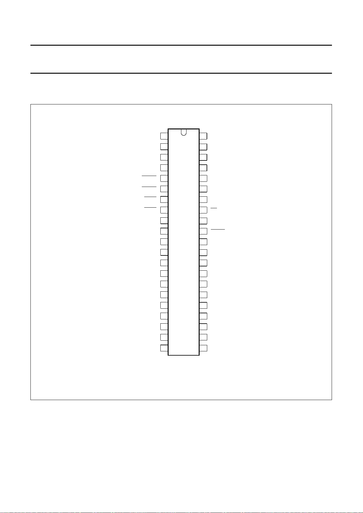
5 PINNING INFORMATION
5.1 Pinning
handbook, halfpage
DP22/VOW1
DP23/VOW0
VOB
VOW2
VSYNC
HSYNC
P10/DXWR
P11/DXRD
DP13/TDAC
P12/DXALE
T3
P14/DXINT
P00
P01
P02
P03
1
2
3
4
5
6
7
8
9
10
PCA84C646
11
PCA84C846
12
13
14
15
16
V
42
41
C
40
DP20/SDA
39
DP21/SCL
DP10/AFC0
38
37
DP11/AFC1
DP12/AFC2
36
35
INT/T0
34
T1
33
RESET
32
XTAL2
31
XTAL1
TEST/EMU
30
29
DP00/PWM00
28
DP01/PWM01
DP02/PWM02
27
PCA84C646; PCA84C846
DD
17
P04
18
P05
19
P06
20
P07
V
21
SS
Fig.2 Pin configuration PCA84C646P and PCA84C846P (SDIP42; SOT270-1).
1995 Jun 15 6
MED171
26
DP03/PWM03
25
DP04/PWM04
24
DP05/PWM05
23
DP06/PWM06
22
DP07/PWM07

Philips Semiconductors Preliminary specification
Microcontrollers for TV tuning
PCA84C646; PCA84C846
control and OSD applications
5.2 Pin description
Table 1 Pin description for PCA84C646P and PCA84C846P; SDIP42 (see Fig.2)
SYMBOL PIN DESCRIPTION
VOB 1 Video fast blanking output signal.
VOW2 2 Video character outputs or derivative port lines.
DP22/VOW1 3
DP23/VOW0 4
VSYNC 5 Vertical synchronization signal input, active LOW.
HSYNC 6 Horizontal synchronization signal input, active LOW.
DXWR 7 Port line 10 or emulation DXWR signal input.
P10/
DXRD 8 Port line 11 or emulation DXRD signal input.
P11/
DP13/TDAC 9 Derivative I/O port or 14-bit D/A PWM.
P12/DXALE 10 Port line 12 or emulation DXALE signal input.
T3 11 Secondary 8-bit counter input pin (Schmitt-trigger).
P14/DXINT 12 Port line 14 or emulation DXINT signal input.
P00 to P07 13 to 20 General I/O port lines (10 mA).
V
SS
DP00/PWM00 to DP07/PWM07 29, 28, 27, 26,
TEST/EMU 30 Control input of testing and emulation mode, normally LOW.
XTAL1 31 Oscillator input terminal for system clock.
XTAL2 32 Oscillator output terminal for system clock.
RESET 33 Initialize input, active LOW.
T1 34 Direct testable pin and event counter input.
INT/T0 35 External interrupt/direct testable pin.
DP12/AFC2 36 Derivative I/O port or comparator input with 4-bit DAC.
DP11/AFC1 37
DP10/AFC0 38
DP21/SCL 39 Derivative port line or I
DP20/SDA 40 Derivative port line or I
C 41 External capacitor input for on chip PLL OSD oscillator.
V
DD
21 Ground.
Derivative I/O port;
25, 24, 23, 22
42 Power supply.
6-bit PWM (PWM04 to 07) or 7-bit PWM (PWM00 to 03).
2
C-bus clock line.
2
C-bus data line.
1995 Jun 15 7

Philips Semiconductors Preliminary specification
Microcontrollers for TV tuning
control and OSD applications
6 RESET
The RESET pin is used as an active LOW input to initialize
the microcontroller to a defined state.
A Power-on-reset can be generated by using the
RC-circuit as shown in Fig.3.
An active reset can be generated by driving theRESET pin
from an external logic device. Such an active reset pulse
should not fall off before VDD has reached its
f
-dependent minimum operating voltage.
xtal
6.1 Reset trip level
RESET trip-voltage level is masked to 1.3 V in the
The
PCA84C646 and PCA84C846.
6.2 Reset status
• Derivative Registers status; for details see Table 40
• Program Counter: 00H
• Memory Bank: 00H
• Register Bank: 00H
• Stack Pointer: 00H
• All interrupts disabled
• Timer/event counter 1 stopped and cleared
• Timer prescaler modulo-32 (PS = 0)
• Timer flag cleared
• Serial I/O interface disabled (ESO = 0) and in slave
receiver mode
• Idle and Stop mode cleared.
PCA84C646; PCA84C846
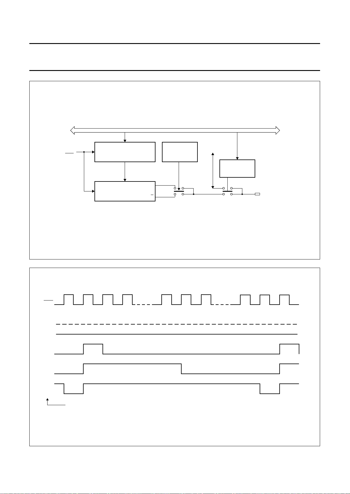
7 ANALOG CONTROL
7.1 6 and 7-bit PWM outputs (PWM00 to PWM07)
The PCA84C646/PCA84C846 has eight PWM outputs for
analog controls of e.g. volume, balance, brightness and
saturation. These PWM outputs generate pulse patterns
with a repetition rate of
analog value is determined by the ratio of the HIGH-time
and the repetition time. A DC voltage proportional to the
PWM control setting is obtained by means of an external
integration network (low-pass filter).
The eight PWM outputs are specified as follows:
• PWM00 to PWM03 outputs with 7-bit resolution
• PWM04 to PWM07 outputs with 6-bit resolution.
Figure 4 shows the block diagram of the 6-bit or 7-bit PWM
DAC. The polarity of the PWM0n output is selected as
shown in Table 2 by the polarity control bit P6LVL/P7LVL
(Derivative Register 23; see Table 25).
The PWM0n output shares the pin with a DP0n I/O line
under control of a PWMnE enable bit; for selection see
Table 3.
Figure 5 shows the 6 and 7-bit PWM0n output patterns
(non-inverted; P6LVL/P7LVL = 0).
The HIGH-time of a PWM0n output is
t
= [PWMnDL]×t
HIGH
where:
[PWMnDL] = the contents of PWMn data latch
(n = 0 to 7; Derivative Register 10 to 17; see Table 40)
t0= 1/f
PWM
; f
PWM
1
⁄64× f
0
=1⁄3× f
xtal
PWM
.
or1⁄
128
× f
PWM
. The
V
DD
R
RESET
( 100 kΩ)
RESET
C
RESET
V
SS
(1) To avoid overload of the internal diode, an external
diode should be added in parallel if C
Fig.3 External components for RESET pin.
1995 Jun 15 8
Table 2 Polarity selection for the PWM0n output
P6L VL/P7LVL POLARITY
(1)
internal reset
1 inverted
0 not inverted
Table 3 Selection of pin function: DP0n/PWM0n (note 1)
PWMnE FUNCTION
PCA84C646/846
MED172
1 PWM0n output
0 DP0n I/O
Note
RESET
> 0.2 µF.
1. n = 0 to 7.
Philips Semiconductors Preliminary specification
Microcontrollers for TV tuning
control and OSD applications
handbook, full pagewidth
f
PWM =
xtal
3
6 or 7-BIT PWM DATA LATCH
6 or 7-BIT DAC PWM
CONTROLLER
f
Q
Q
P6LVL/P7LVL
(1-BIT)
PCA84C646; PCA84C846
DP0n data
I/O
PWMnE
DP0n/PWM0n
MED177
f
handbook, full pagewidth
xtal
3
64
or
128
00
01
m
63
or
127
Fig.4 Block diagram of 6-bit or7-bit PWM DAC.
1 2 3 m m + 1 m + 2
decimal value PWM data latch
64
or
128
1
MLC261
1995 Jun 15 9
Fig.5 Example PWM0n output patterns (P6LVL/P7LVL = 0).

Philips Semiconductors Preliminary specification
Microcontrollers for TV tuning
control and OSD applications
7.2 VST control 14-bit PWM DAC
The PCA84C646 and PCA84C846 have a PWM DAC
output (TDAC) with a resolution of 16384 levels for
Voltage Synthesized Tuning (VST).
Figure 6 shows the block diagram of the 14-bit PWM DAC
which consists of:
• Two 7-bit DAC interface latches (see Table 40):
– VSTH: Derivative Register 18; address 18H.
– VSTL: Derivative Register 19; address 19H.
• One 14-bit DAC data latch: VSTREG, which contents
defines the HIGH-time.
• 14-bit counter.
• Pulse control.
The contents of the interface latches VSTH and VSTL are
latched into VSTREG. The upper seven bits of VSTREG
are used for coarse adjustment, while the lower seven bits
are used for fine adjustment.
The contents of the interface latches VSTH and VSTL are
latched into VSTREG at the beginning of the first t
VSTL is written (see Fig.7). After VSTH and VSTL are
latched into VSTREG, it takes one t
to generate the
sub
appropriate pulse pattern.
Therefore, to ensure correct digital-to-analog conversion,
two t
periods should be allowed before beginning the
sub
next sequence (changing the contents of VSTH and
VSTL).
To ensure that the correct data is latched into VSTREG,
VSTH must contain the correct value before VSTL is
written; see the note in Fig.7.
The repetition times of the pulse controllers are:
• Coarse, upper seven bits (VSTH):
t
sub
128 3 f
⁄×=
xtal
• Fine, lower seven bits (VSTL):
128 t
t
r
× 49152 f
sub
⁄==
xtal
Output TDAC shares the same pin as DP13; bit TDACE
(Derivative Register 22; see Table 22) selects the function
of pin DP13/TDAC.
Table 4 Selection of pin function DP13/TDAC
TDACE FUNCTION
1 TDAC; 14-bit PWM output
0 DP13
sub
after
PCA84C646; PCA84C846
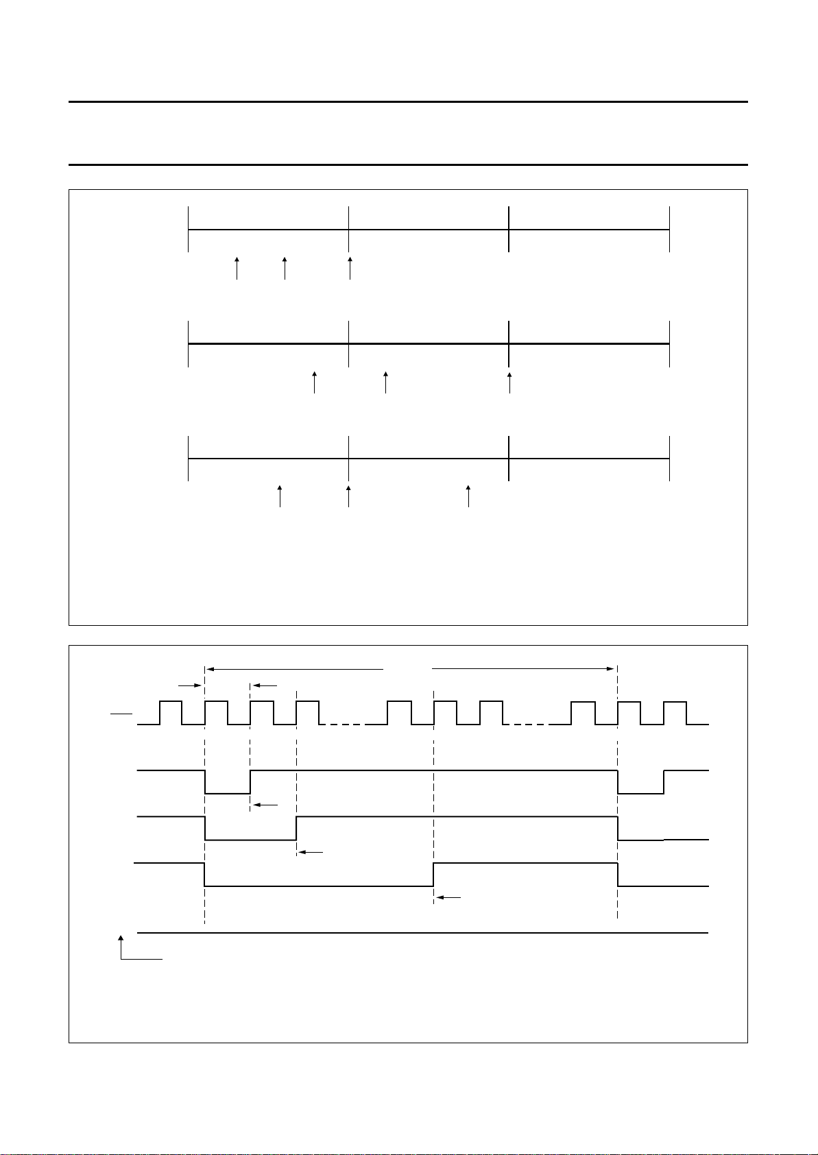
7.2.1 C
An active HIGH pulse is generated in every subperiod; the
pulse width being determined by the contents of VSTH.
The coarse output (OUT1) is LOW at the start of each
subperiod and will remain LOW during
≤
t
s
Where ts is the time within t
The output will then go HIGH and remain HIGH until the
start of the next subperiod. The coarse pulse width may be
calculated as: .
7.2.2 F
Fine adjustment is achieved by generating an additional
pulse in specific subperiods. The pulse is added at the
start of the selected subperiod and has a pulse width of
3/f
xtal
subperiods a fine pulse will be added. It is the logic 0 state
of the value held in VSTL that actually selects the
subperiods. When more than one bit is a logic 0 then the
subperiods selected will be a combination of those
subperiods specified in Table 5. For example, if
VSTL = 111 1010 then this is a combination of:
• VSTL = 111 1110: subperiod 64 and
• VSTL = 111 1011: subperiods 16, 48, 80 and 112.
Pulses will be added in subperiods 16, 48, 64, 80 and 112.
This example is illustrated in Fig.9.
When VSTL holds 111 1111 fine adjustment is inhibited
and the TDAC output is determined only by the contents of
VSTH.
Table 5 Additional pulse distribution
111 1110 64
111 1101 32 and 96
111 1011 16, 48, 80 and 112
111 0111 8, 24, 40, 56, 72, 88, 104 and 120
110 1111 4, 12, 20, 28, 36, 44, 52...116 and 124
101 1111 2, 6, 10, 14, 18, 22, 26, 30...122 and 126
011 1111 1, 3, 5, 7, 9, 11, 13, 15, 17...125 and 127
OARSE ADJUSTMENT
VSTH 1+()3×
------------------------------------------f
xtal
.
subn
3
Pulse duration 127 VSTH–()
INE ADJUSTMENT
×=
-------f
xtal
. The contents of VSTL determine in which
VSTL ADDITIONAL PULSE IN SUBPERIOD
1995 Jun 15 10

Philips Semiconductors Preliminary specification
Microcontrollers for TV tuning
control and OSD applications
‘MOVE instruction’
DAC INTERFACE
7-BIT DATA LATCH
(VSTH)
DATA LOAD
TIMING PULSE
Internal data bus
MSB LSB
DAC INTERFACE
7-BIT DATA LATCH
7
LOAD
(1)
COARSE 7-BIT
14-BIT DATA LATCH
(VSTREG)
7 7
PWM
OUT2OUT1
PCA84C646; PCA84C846
‘MOV instruction’
(VSTL)
7
FINE
ADDITIONAL
PULSE
GENERATOR
(1) See Fig.7 for timing.
PWM output polarity
control bit
P14LVL
ADD
Q
Q14 to 8 Q7 to 1
14-BIT COUNTER
Q
MED179
Fig.6 Block diagram of the 14-bit PWM DAC.
TDAC output
f = f
TDAC xtal
3
1995 Jun 15 11
Philips Semiconductors Preliminary specification
Microcontrollers for TV tuning
control and OSD applications
t
CASE 1
CASE 2
CASE 3
sub
VSTH VSTL
t
sub
t
sub
VSTL
VSTH VSTL
t
sub
VSTH,VSTL is loaded into VSTREG
t
sub
t
sub
VSTH,VSTL is loaded VSTH
into VSTREG
PCA84C646; PCA84C846
t
sub
t
sub
VSTH,VSTL is loaded into VSTREG
t
sub
MED180
In CASE 1 and CASE 2, a new value for VSTH, VSTL is latched into VSTREG.
In CASE 3, VSTL, together with an old value of VSTH are latched into VSTREG.
Fig.7 Latching VSTH, VSTL into VSTREG.
handbook, full pagewidth
f
xtal
3
127 m m + 2
00
01
m
127
decimal value VSTH data latch
3/f
xtal
01
(1)
2 m + 1
(1)
t
subn
127 1
(1)
0
MGC573
(1) t
-------------------------------------------
s
f
xtal
VSTH 1+()3×
=
Fig.8 TDAC output (not inverted) with coarse adjustment only; VSTL = 1111111; P14LVL = 0.
1995 Jun 15 12

Philips Semiconductors Preliminary specification
Microcontrollers for TV tuning
control and OSD applications
handbook, full pagewidth
111 1110
111 1101
111 1011
111 1010
VSTL
t
sub0
t
sub16
t
sub32
t
sub48
t
t
sub64
PCA84C646; PCA84C846
r
t
sub80
t
sub96
t
sub112
t
sub127
MCD314
handbook, full pagewidth
f
xtal
3
127 m
00
01
m
127
3/f
xtal
0
decimal value VSTH data latch
1
Fig.9 Fine adjustment output (OUT2).
t
sub16
2
m + 1
m + 2
127 1
0
MGC572
VSTL = 111 1010; Additional pulses in subperiods 16, 48, 64, 80 and 112.
Fig.10 Example of TDAC (not inverted) output pulses for several values of VSTH (t
1995 Jun 15 13
sub16
).

Philips Semiconductors Preliminary specification
Microcontrollers for TV tuning
control and OSD applications
8 AFC INPUT
The AFC input is intended to measure the level of the
Automatic Frequency Control (AFC) signal. This is done
by comparing the AFC signal with the output of a 4-bit
digital-to-analog converter as shown in Fig.11. The DAC
analog switches select one of the 16 resistor taps that are
connected between VDD and VSS (controlled by bits
AFCV3, AFCV2, AFCV1, AFCV0; Derivative Register 20).
The AFCC signal (bit 0 in Derivative Register 20) then can
be tested to check whether the AFC input is higher or lower
than the DAC level.
The AFC inputs AFC0, AFC1 and AFC2 share the same
pins as Derivative Port lines DP10, DP11 and DP12. The
pin functions are selected by bits AFCE0, AFCE1, AFCE2
(AFC enable/disable bits; Derivative Register 22); for
selection see Table 6.
AFCH1 and AFCH0 (Derivative Register 20) select one
out of three AFC inputs to the comparator; for a correct
comparison, enable the corresponding AFC input (AFCi)
as shown in Table 7.
The conversion time of the AFC is greater than 6 µs but
less than 9 µs. It is recommended to add a NOP instruction
between the instruction which changes V
selection and the instruction which reads the AFCC bit
(compare bit).
or channel
ref
PCA84C646; PCA84C846
If the compare bit:
• AFCC = 0, then the AFC voltage < V
• AFCC = 1, then the AFC voltage > V
Table 6 Selection of pin function DP1i/AFCi (i = 0, 1, 2)
BIT VALUE PIN FUNCTION COMPARATOR
AFCE2 1 DP12 disabled
0 AFC2 enabled
AFCE1 1 DP11 disabled
0 AFC1 enabled
AFCE0 1 DP10 disabled
0 AFC0 enabled
Table 7 AFC input selection
AFCH1 AFCH0 SELECT
0 0 AFC Channel 0; AFC0
0 1 AFC Channel 1; AFC1
1 0 AFC Channel 2; AFC2
1 1 reserved
ref
ref
.
.
handbook, full pagewidth
DP10/AFC0
AFC
DP11/AFC1
DP12/AFC2
Channel selection
AFCE0 AFCE1 AFCE2
ANALOG
SELECTOR
AFCH1 AFCH0
AFC function enable
selection
ENABLE
SELECTOR
Fig.11 AFC circuit.
1995 Jun 15 14
AFCV3
(DP10 to DP12)
EN1 EN2EN0
COMPARATOR
EN
4-BIT D/A
AFCV2 AFCV1 AFCV0
AFC value selection
Internal bus
‘MOV A, D20’
instruction
to read AFCCx bit
MED185

Philips Semiconductors Preliminary specification
Microcontrollers for TV tuning
control and OSD applications
Table 8 V
AFCV3 AFCV2 AFCV1 AFCV0 V
0000 V
0001 V
0010 V
0011 V
0100 V
0101 V
0110 V
0111 V
1000 V
1001 V
1010 V
1011 V
1100 V
1101 V
1110 V
1111 V
as a function of AFCV3 to AFCV0
ref
DD
DD
DD
DD
DD
DD
DD
DD
DD
DD
DD
DD
DD
DD
DD
ref
×1⁄
×2⁄
×3⁄
×4⁄
×5⁄
×6⁄
×7⁄
×8⁄
×9⁄
×10⁄
×11⁄
×12⁄
×13⁄
×14⁄
×15⁄
DD
PCA84C646; PCA84C846
V
(VDD= 5.0 V)
ref
16
16
16
16
16
16
16
16
16
16
16
16
16
16
16
0.31 V
0.62 V
0.93 V
1.25 V
1.56 V
1.87 V
2.18 V
2.50 V
2.81 V
3.12 V
3.43 V
3.75 V
4.06 V
4.37 V
4.68 V
5.00 V
1995 Jun 15 15

Philips Semiconductors Preliminary specification
Microcontrollers for TV tuning
control and OSD applications
9 OSD (ON SCREEN DISPLAY) FUNCTION
9.1 Features
• Display RAM: 64 × 10 bit.
• Display character fonts: 64 (in which 62 customized +
2 special reserved codes).
• Display starting position (of the first character):
64 different positions by software control, both vertical
and horizontal.
• Character size: 4 different character sizes, line-by-line
basis, 1 dot = 1H/1V, 2H/2V, 3H/3V, 4H/4V.
• Character matrix: 12 × 18 with no spacing between
characters.
• Foreground colours: 8, combination of Red, Green, Blue;
character-by-character basis.
• Background/shadowing modes: 4, No background,
Box shadowing, North-west shadowing,
Frame shadowing (raster blanking), frame basis.
• Background colours: 8, combination of Red, Green,
Blue; word-by-word basis. Available when background
mode is either in Box shadowing or North-west
shadowing and Frame shadowing mode.
• On-chip OSD oscillator.
• Character blinking rate: 1 : 1, 1 : 3, 3 : 1 (frequency:
1
⁄16,1⁄32,1⁄64 or1⁄
e.g. NTSC:60⁄16Hz, PAL:50⁄64Hz etc.); character basis.
• Display format: flexible display format by using Carriage
Return (CR) code, maximum number of characters per
line is flexible and depending on the OSD clock.
• Spacing between lines: 4 different choices from 0, 4,
8 or 12 horizontal scan lines.
• Display character RAM auto-address-post-increment
when writing data.
• Programmable HSYNC and VSYNC active input polarity.
• Programmable G (VOW1), B (VOW2), R (VOW0) and
FB (VOB) output polarity.
9.2 Horizontal display position control
The horizontal position counter is increased every OSD
clock (f
) cycle after the programmed level of HSYNC
OSD
occurs at the HSYNC pin and is reset when the opposite
polarity of the HSYNC is reached. Horizontal start position
is controlled by Derivative Register 36 (HPOS;
see Table 36). The starting position is calculated as:
HP = [4 × (H5 to H0) + 5] × (OSD clock cycle)
where (H5 to H0) = decimal value of register HPOS;
(H5 to H0) ≥ 10.
128
of f
, programmable,
VSYNC
PCA84C646; PCA84C846
9.3 Vertical display position control
The vertical position counter is increased every HSYNC
cycle and is reset by the VSYNC signal. Vertical start
position is controlled by Derivative Register 35 (VPOS;
see Table 34). The vertical starting position is calculated
as:
VP = [4 × (V5 to V0)] × (horizontal scan lines)
where (V5 to V0) = decimal value of register VPOS;
(V5 to V0) ≥ 0.
9.4 Clock generator
Figure 12 illustrates the block diagram of the on-chip OSD
clock generator which consists of a Phased-Lock Loop
(PLL) circuit. The Voltage Controlled Oscillator (VCO)
outputs a clock (f
8 to 20 MHz (see Fig.12). The input signal f1= HSYNC.
The programmable active level detector:
• Passes signal f1, when HSYNC is active HIGH, or
• Inverts signal f1, when HSYNC is active LOW.
The output signal f2 is always active HIGH. The VCO is
synchronized with the HIGH-to-LOW edge of the f2 signal.
The value programmed in the 7-bit PLL Programmable
Counter control register (PLLCN; Derivative Register 25;
see Table 40) determines:
f
VCO=f1
×16 × (decimal value of 7-bit counter);
where 16< (decimal value of 7-bit counter) < 48.
The value 16 is the 4-bit prescaler which increases or
decreases the output of the VCO in steps of (16 × f1).
Given an example of f1= 15.750 kHz, the f
increased or decreased in steps of
16 × 15.750 kHz = 252 kHz = 0.25 MHz.
The f
is fed into a buffer to generate the OSD dot clock
VCO
frequency signal (f
Decreasing f
OSD
Recommended: 4 MHz ≤ f
The OSD clock is enabled/disabled by the state of the EN
bit (Derivative Register 34; see also Section 12.4). When
the OSD clock is disabled (f
remains active, therefore the transient time from the OSD
clock start-up to locking into the external HSYNC signal is
reduced.
As the on-chip oscillator is always active after Power-on,
when the OSD clock is enabled no large currents flow (as
for RC or LC oscillators) and therefore radiated noise is
dramatically reduced.
) with a frequency range of
VCO
); 4 MHz ≤ f
OSD
OSD
≤ 12 MHz.
gives broader characters.
typical ≤ 12 MHz.
OSD
= LOW) the oscillator
OSD
VCO
is then
1995 Jun 15 16

Philips Semiconductors Preliminary specification
Microcontrollers for TV tuning
control and OSD applications
9.4.1 MOUNTING PRECAUTIONS
To achieve good OSD performance, take the following
precautions for the microcontroller mounting:
• Apply the recommended R, Cs and Cp (PLL loop filter)
values as shown in Fig.12 and place them as close as
possible to pin C (41).
• To guarantee stable PLL operation, apply a noise-free
HSYNC signal (pin 6).
• Avoid heavy loading of the output pins.
• The supply voltage (VDD) must be correctly decoupled.
Connect decoupling capacitors as close as possible to
the VDD and VSS pins.
handbook, full pagewidth
f
1
HSYNC
ACTIVE
LEVEL
DETECTOR
f
2
FREQUENCY
(2)
PROGRAMMABLE
STANDBY
PHASE/
DETECTOR
divided by N
7-BIT COUNTER
PCA84C646; PCA84C846
• Position microcontroller optimal and away from
components bearing high voltage and/or strong current.
• PLL loop filter ground of capacitors C
directly connected to the VSS pin (21). Avoid a ground
loop and separate the ground from other digital signals
ground.
• The connection between VSS pin (21) and +5 V regulator
ground/switching power supply secondary ground must
be as short as possible.
CHARGE PUMP
AND
LOOP FILTER
f
16
VCO
VOLTAGE
CONTROLLED
OSCILLATOR
C
and Cp must be
s
(1)
R
C
s
C
p
f
OSD
(OSD clock)
(1) R=10to47kΩ; typ. 15 kΩ.
= 100 to 470 nF; typ. 220 nF.
C
s
=1⁄10Cs.
C
p
For mounting see Section 9.4.1 “Mounting precautions”.
(2) Example:
= 15.750 kHz and (decimal value of 7-bit counter) = 32 then f
If f
1
and the output of the Programmable 7-bit counter is 15.750 kHz.
VCO
Fig.12 On-chip OSD oscillator.
1995 Jun 15 17
= 8.064 MHz
OSD disable
MED196
Philips Semiconductors Preliminary specification
Microcontrollers for TV tuning
control and OSD applications
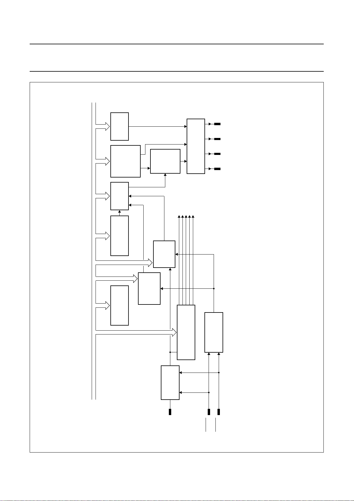
CONTROL
REGISTER
RAM
DISPLAY
CHARACTER
BUFFER
ADDRESS
SELECTOR
BIT
DISPLAY
PATTERN
DISPLAY CONTROL
ROM(64)
control
signals
PCA84C646; PCA84C846
MED189
AND
OUTPUT STAGE
RGBFB
VOW1 VOW0 VOW2 VOB
CPU bus
COUNTER
WRITE ADDRESS
POSITION
HORIZONTAL
CONTROL
CHARACTER SIZE
POSITION
VERTICAL
REGISTER/
COUNTER
REGISTER/
ON-CHIP
C
COUNTER
CONTROL REGISTER
INSTRUCTION DECODER
OSCILLATOR
CIRCUIT
INTERNAL
SYNCHRONOUS
handbook, full pagewidth
Fig.13 OSD block diagram.
1995 Jun 15 18
HSYNC
VSYNC

Philips Semiconductors Preliminary specification
Microcontrollers for TV tuning
PCA84C646; PCA84C846
control and OSD applications
10 DISPLAY RAM ORGANIZATION
The display RAM is organized as 64 × 10 bits.
The general format of each RAM location is as follows:
• Bits <9-4> hold data, comprising:
– Customer designed Character Font Codes (62)
– Carriage Return Code (1)
– Space Code (1).
• Bits <3-0> contain the attributes of the Character Font:
– Foreground colour and Blinking
– Character size and Line space
– Background colour and End-of-Display .
Table 9 Format of Character Font Code
987654321 0
C5 C4 C3 C2 C1 C0 T3 T2 T1 T0
Character Font Code (00H - 3DH) Foreground colour Blink
10.1 Description of display RAM codes
There are three data formats for the display RAM code
1. Character Font Code
2. Carriage Return Code
3. Space Code.
The three data formats and their descriptions are shown in
Tables 9 to 17. Figure 14 illustrates an example of the
timing of FB, R, G, and B pulses when displaying a line of
dots stream in a character.
FB = VOB; R = VOW0, G = VOW1; B = VOW2.
Figure 15 shows an example of the screen which includes
some Cariage Return and Space codes.
Table 10 Description of Character Font Code bits
SYMBOL DESCRIPTION
C5 to C0 If bits <9-4> are in the range (00H to 3DH), then this is a Character Font Code and 1 from 62 customer
designed character fonts can be selected.
T3 to T1 Bits <3-1> determine the (Foreground) colour (1 out of 8) of this character; see Table 11.
T0 Blinking of this character is controlled by bit <0>. See Section 12.3 for duty cycle and frequency control.
When T0 = 0; blinking is OFF.
When T0 = 1; blinking is ON. Blinking rate:
Table 11 Selection of Background and Foreground colour
T3
(RED)
0 0 0 black
0 0 1 blue
0 1 0 green
0 1 1 cyan
100red
1 0 1 magenta
1 1 0 yellow
1 1 1 white
T2
(GREEN)
1
⁄16,1⁄
32
,1
⁄64or1⁄
128
T1
(BLUE)
× f
VSYNC
.
COLOUR
1995 Jun 15 19

Philips Semiconductors Preliminary specification
Microcontrollers for TV tuning
PCA84C646; PCA84C846
control and OSD applications
Table 12 Format of Carriage Return Code
9876543210
C5 C4 C3 C2 C1 C0 T3 T2 T1 T0
Carriage Return Code (3EH) Character size Line Spacing
Table 13 Description of Carriage Return Code bits; format is shown in Table 12
SYMBOL DESCRIPTION
C5 to C0 If bits <9-4> hold 3EH, then this is the Carriage Return Code. The current display line is terminated
(a transparent pattern appears on the screen) and the next character will be displayed at the beginning of
the next line.
T3 to T2 Bits <3-2> select the size of the of the character to be displayed on the next line; see Table 14.
T1 to T0 Bits <1-0> determine the spacing between lines of displayed characters. Spacing is a multiple of the
number of horizontal scan lines. In order to prevent vertical jumping of the display, the first line should be
a non-displayed line i.e. the Carriage Return Code.
The line spacing for this code must not be zero; see Table 15.
Table 14 Selection of character size
T3 T2 CHARACTER DOT SIZE
0 0 1H/1V
0 1 2H/2V
1 0 3H/3V
1 1 4H/4V
(1)
Table 15 Selection of line spacing
T1 T0 LINE SPACING
0 0 0H line
0 1 4H line
1 0 8H line
1 1 12H line
Note
1. H is the OSD clock period; V is the number of
horizontal scan lines per dot.
Table 16 Format of Space Code
987654321 0
C5 C4 C3 C2 C1 C0 T3 T2 T1 T0
Space Code (3FH) Background colour End
Table 17 Description of Space Code bits; format is shown in Table 16
SYMBOL DESCRIPTION
C5 to C0 If bits <9-4> hold 3FH, then this is the Space Code. A transparent pattern, equal to one character width,
will be displayed on the screen.
T3 to T1 Bits <3-1> determine the background colour of the characters including the Space Code in Box
shadowing mode but following the Space Code in North-west shadowing mode. See Section 12.4 for
more details. Background colour selection is the same as Foreground colour selection; see Table 11.
T0 Bit <0> is the End-of-Display bit and indicates the end of display of the current screen before exhaustion
of display RAM. The last character displayed on the TV screen is either the 64
Code with the End-of-display attribute set to logic 1.
When T0 = 0; continue display of next character.
When T0 = 1; end of display.
th
RAM location or a Space
1995 Jun 15 20

Philips Semiconductors Preliminary specification
Microcontrollers for TV tuning
control and OSD applications
handbook, full pagewidth
R
G
B
I
FB
ACM
"S" : red colour "E" : B+I colour
"I" : green colour 1st SP code : ACM = on
"Z" : G+B+I colour 2nd SP code : ACM = off
PCA84C646; PCA84C846
SP code SP code
MED204
handbook, full pagewidth
line spacing 1 = 4H
line spacing 2 = 8H
Fig.14 R, G, B and FB timing.
Vstart
HI ! THIS ISSP SP CR
CR
T H E N E W
F U N C I O NT
I N P C F 8 5 C X X
Hstart
St andal
SP
Volume
Four different background colours (in box shadowing mode):
Channel
Black
Red
Green
Blue
SP
SP
E L C O M EW
CR
CR
CR
X
line spacing 3 = 0H
line spacing 4 = 0H
CR
line spacing 4 = 4H
line spacing 6 = 0H
CR
MED205
1995 Jun 15 21
Fig.15 On-screen-display (an example).
 Loading...