


查询PCA84C122供应商
INTEGRATED CIRCUITS
DATA SH EET
PCA84C122; 222; 422; 622; 822
8-bit microcontrollers for
remote control transmitters
Product specification
Supersedes data of February 1994
File under Integrated Circuits, IC14
Philips Semiconductors
1995 May 01

Philips Semiconductors Product specification
8-bit microcontrollers for
remote control transmitters
CONTENTS
1 FEATURES
2 GENERAL DESCRIPTION
2.1 Important note
3 MEMORY AND I/O CONFIGURATIONS
4 ORDERING INFORMATION
5 BLOCK DIAGRAM
6 PINNING INFORMATION
6.1 Pinning
6.2 Pin description
7 POWER-ON-RESET STATUS AND PORT
OPTIONS
8 HARDWARE MODULATOR
8.1 Interface between the 84CXXX core and
derivative logic
8.2 Instructions for data transfer between the
84CXXX core and derivative logic
8.3 Operation of the Hardware Modulator
9 INTERRUPTS
9.1 Internal timer/counter
9.2 External keypad wake-up and T0/INT pin
10 OUTPUT DRIVER
11 WATCHDOG TIMER (WDT)
12 LIMITING VALUES
13 DC CHARACTERISTICS
14 AC CHARACTERISTICS
15 APPLICATION INFORMATION
16 PACKAGE OUTLINES
17 SOLDERING
17.1 Plastic small outline packages
17.2 Plastic dual in-line packages
18 DEFINITIONS
19 LIFE SUPPORT APPLICATIONS
PCA84C122; 222; 422; 622; 822
1995 May 01 2

Philips Semiconductors Product specification
8-bit microcontrollers for
remote control transmitters
1 FEATURES
• 84CXXX CPU
• ROM, RAM and I/O configurations are device
dependent; see Chapter 3
• Two test inputs: T0 (ANDed with Port 1 input lines)
and T1
• 3 single-level vectored interrupt sources:
– external (T0/INT and Port 1, for keypad press
wake-up function)
– timer/counter (TI)
– hardware modulator interrupt
• 8-bit programmable timer/counter with 5-bit pre-scaler
• Power saving: Idle and Stop modes are provided
• Hardware Modulator providing pulse bursts, with:
– programmable duty factor for each pulse
– programmable number of pulses
• One output line from the Hardware Modulator to control
the driver transistor for the infrared LED (IR-LED).
Capable of sinking 27 mA at V
• Watchdog Timer to keep the transmitter from being
locked or malfunction
• Available packages: SO and DIP types (SO20, SO24,
SO28, SDIP24 and DIP20); see Chapter 4
• On-chip oscillator: 455 kHz to 6 MHz
• Single supply voltage: 2.0 V to 5.5 V
• Operating temperature: −20 to +50 °C.
2 GENERAL DESCRIPTION
The PCA84C122 is a stand-alone microcontroller
designed for use in remote control transmitters for a wide
range of applications.
The PCA84C122 provides a number of dedicated
hardware functions for remote controller applications.
These functions include the following additional blocks to
the 84CXXX core:
• Interrupt Gate
• Hardware Modulator
• Output Driver
• Watchdog Timer.
= 2.0 V, V
DD
OUT
= 1.0 V
PCA84C122; 222; 422; 622; 822
Although the PCA84C122 is specifically referred to
throughout this data sheet, the information applies to all
the devices. The differences between the PCA84C122
and the other devices are specified in Chapter 3.
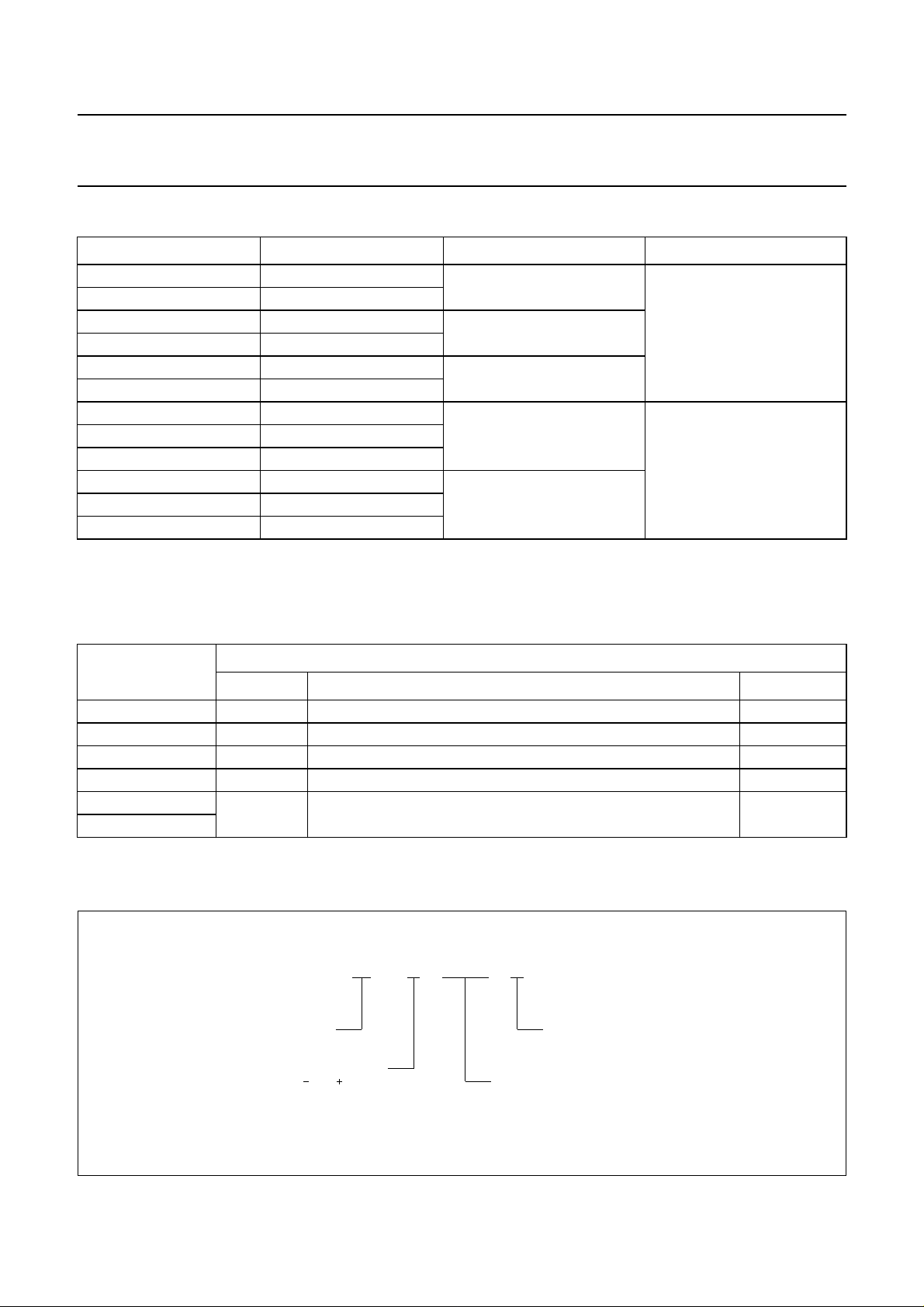
Figure 2 shows the general block diagram of the device.
The 84CXXX core plus 8 kbytes ROM and 64 bytes RAM
has the same function as described in the PCF84CXXX
family description (see
When the transmitter is not in use the microcontroller is in
Stop mode and the oscillator is halted. The AND gate
connected to the Port 1 (P10 to P17) lines provides the
wake-up to end the Stop mode.
The Hardware Modulator produces pulse bursts according
to the required protocol. The ON-time and OFF-time of
each pulse (i.e. duty factor) and the number of pulses are
controlled by software.
The Watchdog Timer (WDT) will reset the PCA84C122
when it has not been reloaded (reset) in time, because the
program has run out of sequence (endless loop,
continuous Idle mode, etc.). During Stop mode the
oscillator is halted, therefore the Watchdog Timer is not
running.
Automatic system reset is generated by the WDT if the
timer is not reset before overflow from counting within
a certain period of time.
The Output Driver can handle sufficient current to drive a
single transistor, that provides the required current for the
IR-LED.
2.1 Important note
This data sheet details the specific properties of the
PCA84C122; PCA84C222; PCA84C422; PCA84C622
and PCA84C822. The shared characteristics of the family
of microcontrollers are described in the PCF84CXXXA
Family single-chip 8-bit Microcontroller of
IC14”
, which should be read in conjunction with this data
sheet.
“Data Handbook IC14”
).
“Data Handbook
1995 May 01 3
Philips Semiconductors Product specification
8-bit microcontrollers for
remote control transmitters
3 MEMORY AND I/O CONFIGURATIONS
DEVICE I/O LINES ROM RAM
PCA84C122A 16
PCA84C122B 12
PCA84C222A 16
PCA84C222B 12
PCA84C422A 16
PCA84C422B 12
PCA84C622A 16
PCA84C622B 12
PCA84C622C 20
PCA84C822A 16
PCA84C822C 20
Note
1. 4 I/O lines with 10 mA sink capability.
(1)
(1)
PCA84C122; 222; 422; 622; 822
1K
2K
4K
6K
8KPCA84C822B 12
32 bytes
64 bytes
4 ORDERING INFORMATION
TYPE NUMBER
(1)
PACKAGE
NAME DESCRIPTION VERSION
PCA84CX22AP SDIP24 plastic shrink dual in-line package; 24 leads (400 mil) SOT234-1
PCA84CX22AT SO24 plastic small outline package; 24 leads; body width 7.5 mm SOT137-1
PCA84CX22BP DIP20 plastic dual in-line package; 20 leads (300 mil) SOT146-1
PCA84CX22BT SO20 plastic small outline package; 20 leads; body width 7.5 mm SOT163-1
PCA84C622CT
PCA84C822CT
SO28
plastic small outline package; 28 leads; body width 7.5 mm;
low stand-off height
SOT136-1
Note
1. ‘X’ in the type number denotes the numbers: 1, 2, 4, 6 and 8.
technology:
PC = CMOS
temperature range:
A = 20 to 50 C
PC
o
84C122
A
P
package:
P = plastic DIL
T = plastic mini-pack (SO)
generic type number
MLA973 - 1
Fig.1 Numbering scheme.
1995 May 01 4
Philips Semiconductors Product specification
8-bit microcontrollers for
remote control transmitters
5 BLOCK DIAGRAM
XTAL
XTAL1
OSCILLATOR
XTAL2
HARDWARE
MODULATOR
PCA84C122; 222; 422; 622; 822
OUT
DRIVER
OUTPUT
MCD248 - 2
T0/INT
PCA84CXXX
RAM
64 bytes
ROM
8 kbytes
osc
f / 30
DD
V
WDT
CORE
84CXXX
T1
P20
RESET
T0/INT
P21
P22
P23
P17
P16
P15
P14
P13
P12
P11
P10
P07
P06
P05
P04
P03
P02
P01
P00
SS
V
handbook, full pagewidth
Fig.2 Block diagram.
1995 May 01 5
Philips Semiconductors Product specification
8-bit microcontrollers for
remote control transmitters
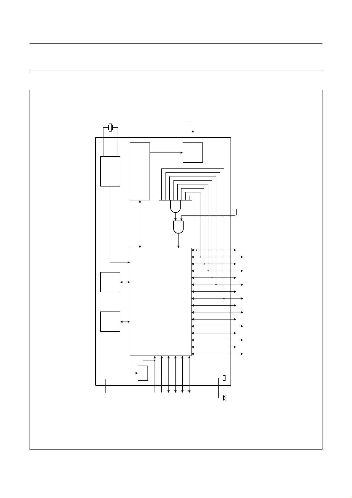
6 PINNING INFORMATION
6.1 Pinning
P14 P15
1
2
P01
P00
3
T0 / INT
RESET
4
T1
5
6
84CX22AP
V
DD
XTAL2
XTAL1
P04
P05
P16 P17
84CX22AT
7
8
9
10
11
12
MCD251 - 2
PCA84C122; 222; 422; 622; 822
1
24
P02
23
P03
22
21
OUT
V
20
SS
P10
19
P11
18
P12
17
P13
16
P07
15
P06
14
13
P22
2
P14
3
P01
4
P00
T0/INT
RESET
XTAL2
XTAL1
5
6
T1
7
84C622CT
V
DD
P04
P05
P16 P17
P20
84C822CT
8
9
10
11
12
13
MLA977 - 1
P23
28
P15
27
P02
26
P03
25
24
OUT
V
SS
23
P10
22
P11
21
P12
20
P13
19
P07
18
P06
17
16
P21
1514
Fig.3 Pin configurations PCA84CX22AP (SDIP24)
and PCA84CX22AT(SO24).
1
P01
2
P00
T1
V
DD
XTAL2
XTAL1
P04
P05
3
4
5
84CX22BT
6
7
8
9
10
MCD250 - 2
T0 / INT OUT
RESET
20
P02
19
P03
18
V
17
SS
16
P10
15
P11
P12
14
P13
13
P07
12
P06
11
Fig.4 Pin configuration PCA84CX22CT (SO28).
1
P10
V
SS
OUT
P03
P02
P01
P00
T0/INT
RESET
T1
2
3
4
5
84CX22BP
6
7
8
9
10
MLA975 - 2
20
P11
19
P12
P13
18
17
P07
P06
16
P05
15
P04
14
XTAL1
13
XTAL2
12
V
11
DD
Fig.5 Pin configuration PCA84CX22BT (SO20). Fig.6 Pin configuration PCA84CX22BP (DIP20).
1995 May 01 6
Philips Semiconductors Product specification
8-bit microcontrollers for
PCA84C122; 222; 422; 622; 822
remote control transmitters
6.2 Pin description
Table 1 Pin description for PCA84CX22AP, PCA84CX22AT, PCA84CX22BP, PCA84CX22BT and PCA84CX22CT
PIN
SYMBOL
P00 to P07 3, 2, 23, 22,
P10 to P17 19, 18, 17, 16,
P20 to P23 − 14, 15, 1, 28 −−standard I/O Port lines, generally
INT4538test T0 and external interrupt input
T0/
T15649test T1 input
RESET 67510active HIGH reset;
SDIP24/SO24
(see Fig.3)
10, 11, 14, 15
1, 22, 12, 13
SO28
(see Fig.4)
4, 3, 26, 25,
11, 12, 17, 18
22, 21, 20,19,
2, 27, 13, 16
SO20
(see Fig.5)
2, 1, 20, 19, 9,
10, 11, 12
16, 15, 14, 13 1, 20,19, 18 standard I/O Port lines, generally
DIP20
(see Fig.6)
7, 6, 5, 4, 14,
15, 16, 17
standard I/O Port lines, generally
used for keypad scanning
used for keypad sensing
used for visible LED’s
normally connected to V
For further information see
PCF84CXXXA description in
“Data Handbook IC14”
XTAL1 9 10 8 13 crystal or ceramic resonator
XTAL289712
OUT 21 24 18 3 pulse train output pin, capable of
sinking 27 mA
V
DD
V
SS
78611power supply
20 23 17 2 ground
DESCRIPTION
.
SS
.
7 POWER-ON-RESET STATUS AND PORT OPTIONS
• All Port lines are standard I/O (option 1).
• RESET (Power-on-reset) level of 1.3 V.
After Power-on-reset, Port 0 is reset to LOW; Port 1, Port 2 and
1995 May 01 7
OUT are reset to HIGH.
Philips Semiconductors Product specification
8-bit microcontrollers for
remote control transmitters
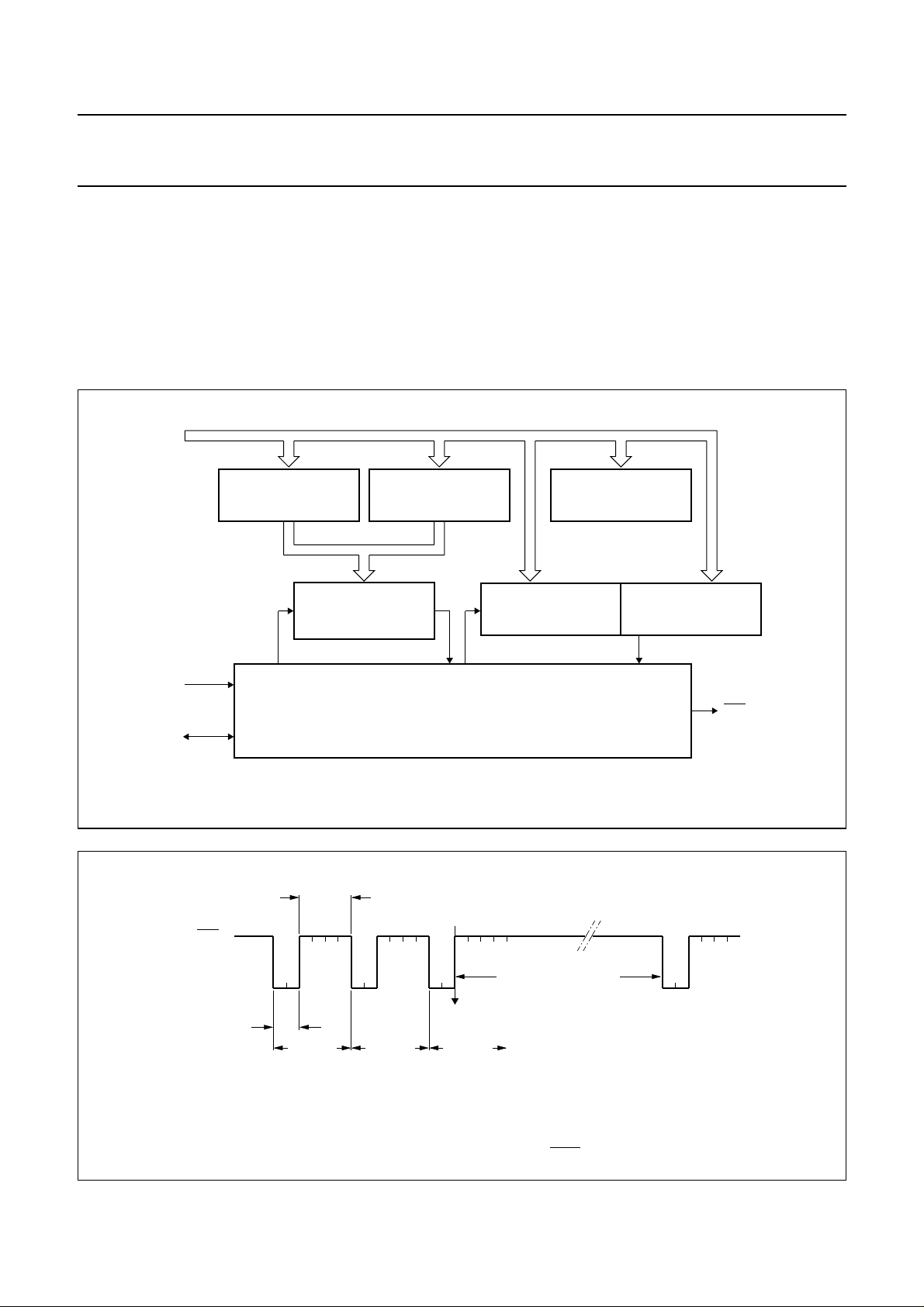
8 HARDWARE MODULATOR
The Hardware Modulator is the main derivative part in the
PCA84C122. Figure 7 shows the internal architecture.
The Hardware Modulator generates a pulse train whereby
the ON-time of a pulse and the OFF-time between pulses
can be programmed in a number of clock cycles
(period = 1/f
); see Figs 8 and 7.
osc
internal bus (IB0 – 7)
ON-TIME
REGISTER
(8)
OFF-TIME
REGISTER
(8)
PCA84C122; 222; 422; 622; 822
The number of pulses of the train is also programmable.
The time between pulse bursts is determined by software,
possibly using the standard 8-bit Timer/Counter.
8.1 Interface between the 84CXXX core and
derivative logic
There are three (derivative) registers and one (derivative)
counter that must be loaded from the core.
CONTROL
REGISTER
(5)
f
osc
control
OUT
start
ON-time
PULSE TIMER
(8)
CONTROL LOGIC
Fig.7 Hardware Modulator.
OFF-time
end
interrupt
pulse #1 pulse #2 pulse #3
PULSE COUNTER
HIGH
(2)
elapse time by software
PULSE COUNTER
LOW
(8)
OUT
MCD255 - 1
MCD254
OFF-time = 4 (off-time register = 2)ON-time = 2 (on-time register = 0) number of pulses = 3
Fig.8 Example pulse train output of OUT pin.
1995 May 01 8

Philips Semiconductors Product specification
8-bit microcontrollers for
PCA84C122; 222; 422; 622; 822
remote control transmitters
8.1.1 ON-TIME REGISTER (ADDRESS: 00H)
This 8-bit register is loaded by software; the decimal value
of its contents + 2, determine the number of oscillator
cycles that the
The active period (ON-time) of
8.1.2 OFF-
OUT pin is active.
contents 2+()
=
OUT
TIME REGISTER (ADDRESS: 01H)
-------------------------------------- f
osc
This 8-bit register is loaded by software; the decimal value
of its contents + 2, determine the number of oscillator
cycles that the
The inactive period (OFF-time) of
OUT pin is inactive.
OUT
contents 2+()
=
-------------------------------------- f
osc
Table 2 Control Register (CR)
76543210
−−−RWDT Rint PWM LgP HF
8.1.3 P
ULSE COUNTER
The Pulse Counter, is a 10-bit register consisting of:
• Pulse Counter Low (8-bit); address 02H.
• Pulse Counter High (2-bit); address 04H.
The Pulse Counter is loaded by software with the number
of pulses required in a pulse burst; loading ‘0’ is not
allowed.
8.1.4 C
ONTROL REGISTER (ADDRESS 03H)
The Control Register contains the bits that control various
possibilities for the output pulses, plus the reset of the
interrupt flip-flop and the Watchdog timer.
Table 3 Description of the CR bits
BIT SYMBOL DESCRIPTION
7to5 − Reserved.
4 RWDT Reload Watchdog Timer: This is not an actual flip-flop in the Control Register. If a logic 1 is
written to this bit position the Watchdog Timer is reloaded (reset to 0); this bit is Write only.
3 Rint Reset Interrupt: This is not an actual flip-flop in the Control Register. If a logic 1 is written to this
bit position the interrupt flip-flop is reset; this bit is Write only.
2 PWM Pulse Width Modulation: Is the standard term for a quasi analog signal. It is a square wave
signal of which the duty cycle may be varied. When integrated a real analog signal may be
obtained. When PWM = 1; the Pulse Counter Register is ignored and a continuous pulse train is
generated (see Fig.9); this bit is Read or Write.
1 LgP Long Pulse: When LgP = 1; the OFF-time Register is ignored and a single pulse of length
ON-time()number of pulses()×=
frequency
1
⁄4× f
(see Fig.10); this bit is Read or Write.
osc
is generated. If HF = 1, this pulse is modulated with a
0HF High Frequency: When HF = 1 the ON-time part of the generated pulse is modulated with a
frequency
1
⁄4× f
(see Fig.11); this bit is Read or Write.
osc
8.2 Instructions for data transfer between the 84CXXX core and derivative logic
INSTRUCTION DESCRIPTION
MOV Dx,A Move contents of the accumulator to the derivative register.
MOV A,Dx Move contents of derivative register to the accumulator.
ANL Dx,A AND derivative register contents with contents of accumulator. Result is stored in derivative register.
ORL Dx,A OR derivative register contents with contents of accumulator. Result is stored in derivative register.
1995 May 01 9

Philips Semiconductors Product specification
8-bit microcontrollers for
remote control transmitters
HF = 0 LgP = 0 PWM = 1 OFF-time = 5ON-time = 3
number of pulses = don' t care
PCA84C122; 222; 422; 622; 822
MCD258
Fig.9 Analog output (PWM).
interrupt
HF = 1 LgP = 1 PWM = 0 OFF-time = don' t careON-time = 12
number of pulses = 5
Fig.10 Long Pulse (modulated).
interrupt
HF = 1 LgP = 0 PWM = 0 OFF-time = 12ON-time = 12
number of pulses = 3
software time
MCD257 - 1
software time
MCD256 - 1
Fig.11 Modulated by1⁄4× f
1995 May 01 10
osc
.

Philips Semiconductors Product specification
8-bit microcontrollers for
remote control transmitters
8.3 Operation of the Hardware Modulator
First the ON-time and OFF-time registers are loaded. The
number of pulses to be generated is stored in the Pulse
Counter. The Hardware Modulator starts as soon as the
Pulse Counter is loaded. First the signal
and the ON-time value is stored in the Pulse Timer. Then
the Pulse Timer is counted down with pulses of 1/f
When the Pulse Timer reaches zero the
becomes inactive and the value held in the Pulse Counter
is decreased by ‘1’. If the Pulse Counter is not yet zero, the
OFF-time is stored in the Pulse Timer and is counted down
again. When it reaches zero now, signal
again, ON-time is loaded and the counter starts counting
down etc. On the Pulse Counter reaching zero, an interrupt
(Special Interrupt, SI) is sent to the CPU, indicating that the
Hardware Modulator is ready.
The delay between two pulse bursts is determined by
software. When a new burst must be generated with the
same ON-time and OFF-time values, only the Pulse
Counter is loaded with the required number of pulses and
the Hardware Modulator will start automatically. The
interrupt signal is reset when the Pulse Counter is loaded
or can be reset directly by writing a logic 1 to bit Rint of the
Control Register.
9 INTERRUPTS
OUT is activated
.
osc
OUT signal
OUT is activated
PCA84C122; 222; 422; 622; 822
If the external interrupt is disabled, program execution
continues with the instruction following the STOP
instruction.
The wake-up function is activated when any of the
sense lines (Port 1 pins) are pulled LOW.
9.2.2 T0/
T0/INT must be connected to VDD when not in use,
because no internal pull-up or pull-down is present
(floating input).
Because this pin is ‘ANDed’ with Port 1 inputs, the result of
‘JTO’ and ‘JNTO’ instructions and the interrupt depends on
the AND of all Port 1 and T0/
T0/INT can serve as an extra sense line, when a pull-up
resistor is connected, however, multiple keys will not be
detected.
10 OUTPUT DRIVER
The output of the Hardware Modulator is amplified and
able to sink a current of 27 mA when the
active. Therefore, only one external (PNP) transistor is
required to drive the IR-LED.
LOW level output sink current, minimum 27 mA at
VDD= 2.0 V, V
INT PIN
OUT
INT inputs.
OUT signal is
< VDD− 1.0 V.
There are three different interrupt sources with different
vectors within the PCA84C122, these are:
• External keypad wake-up and T0/
INT pin;
vector address: 03H
• Hardware modulator (SI); vector address: 05H
• Internal Timer/counter (TI); vector address: 07H.
9.1 Internal timer/counter
The internal timer/counter is the same as in the other
members of the PCF84CXXX family. Instructions
‘EN TCNTI’ and ‘DIS TCNTI’ are to enable/disable
the interrupt.
9.2 External keypad wake-up and T0/
9.2.1 K
EYPAD WAKE-UP
INT pin
The keypad wake-up function generates an interrupt
signal to the CPU. This signal is used to terminate the Stop
mode and thus allows program execution to continue.
If the external interrupt is enabled the microcontroller
executes the instruction immediately following the STOP
instruction, before executing the interrupt routine.
11 WATCHDOG TIMER (WDT)
The Watchdog timer consists of a 17 stage counter with a
clock of
⁄30× f
. A logic 1 written to RWDT bit (Control
osc
1
Register) clears the WDT to zero.
After a Power-on-reset, the WDT is cleared to zero; the
content of the WDT is then incremented by ‘1’ every
30 clock cycles.
If the WDT is not reset to zero before it overflows, a
RESET signal is generated and the device is reset, thus
preventing a lock up or malfunction. The software must
clear the WDT at least 1/f
generates the RESET signal; i.e. at f
× 30 × 216 seconds before it
osc
= 1 MHz, this is
osc
1.92 s.
In the Idle mode the oscillator is still running and therefore
the WDT remains active. In the Stop mode, the WDT is
fully stopped and the value of the counter is kept.
1995 May 01 11

Philips Semiconductors Product specification
8-bit microcontrollers for
PCA84C122; 222; 422; 622; 822
remote control transmitters
12 LIMITING VALUES
In accordance with the Absolute Maximum Rating System (IEC 134).
SYMBOL PARAMETER MIN. MAX. UNIT
V
DD
V
I
I
source(max)
I
sink(max)
I
OUT
I
rev
P
tot
T
stg
T
amb
13 DC CHARACTERISTICS
V
= 4.5 V to 5.5 V; VSS=0V;T
DD
SYMBOL PARAMETER CONDITIONS MIN. TYP. MAX. UNIT
supply voltage −0.5 +7.0 V
all input voltages −0.5 VDD+ 0.5 V
maximum source current (all Port lines) −−5mA
maximum sink current (all Port lines) − 5mA
output current 27 − mA
maximum reverse current −−500 mA
total power dissipation − 500 mW
storage temperature −55 +125 °C
operating ambient temperature −20 +50 °C
= −20 to +50 °C; all voltages with respect to VSS; unless otherwise specified.
amb
Supply
V
DD
I
DD
I
DD(ID)
I
DD(ST)
Inputs (RESET, T0/
V
IL
V
IH
I
Ll
supply voltage 2.0 3.0 5.5 V
operating supply current VDD=3V; f
V
=5V; f
DD
supply current Idle mode VDD=3V; f
V
=5V; f
DD
supply current Stop mode VDD=5V; f
= 3 MHz − 0.4 0.9 mA
xtal
= 3 MHz − 0.9 1.8 mA
xtal
= 3 MHz − 0.20 0.40 mA
xtal
= 3 MHz − 0.25 0.50 mA
xtal
= 3 MHz − 1.20 10 µA
xtal
INT, T1, Port 0: P00 to P07, Port 1: P10 to P17, Port 2: P20 to P23)
LOW level input voltage 0 − 0.3VDDV
HIGH level input voltage 0.7VDD− V
input leakage current VSS< VI< V
DD
Outputs (Port 0: P00 to P07, Port 1: P10 to P17, Port 2: P20 to P23)
I
I
OL
OH
LOW level output sink current VDD=5V; VO= 0.4 V 1.6 12.0 − mA
V
= = 5 V; VO= 0.4 V; P20 − P23 10 −− mA
DD
HIGH level pull-up output source
current
VDD=5V; VO= 0.7V
V
=5V; VO=V
DD
SS
DD
PULSE OUTPUT (OUT)
I
I
OL
OH
LOW level output sink current VDD=2V; VO= 1.0 V 27 −− mA
HIGH level output source current VDD=2V; VO= 0.7V
DD
DD
V
− 0.20 10 µA
−40 −100 −µA
−140 −140 −400 µA
−1.6 −− mA
1995 May 01 12

Philips Semiconductors Product specification
8-bit microcontrollers for
PCA84C122; 222; 422; 622; 822
remote control transmitters
14 AC CHARACTERISTICS
V
= 2.0 V to 5.5 V; VSS=0V;T
DD
SYMBOL PARAMETER CONDITIONS MIN. TYP. MAX. UNIT
Oscillator
f
g
g
g
R
xtal
mL
mM
mH
FB
operating crystal frequency VDD= 2.5 V 0.455 − 6.0 MHz
Low transconductance 0.3 0.7 1.4 mS
Medium transconductance 0.9 1.6 3.2 mS
High transconductance 3.0 4.5 9.0 mS
feedback resistor 0.3 1.0 3.0 MΩ
= −20 to +50 °C; all voltages with respect to VSS; unless otherwise specified.
amb
= 2.0 V 0.455 − 5.0 MHz
V
DD
1995 May 01 13

Philips Semiconductors Product specification
8-bit microcontrollers for
remote control transmitters
15 APPLICATION INFORMATION
P00
P01
P02
P03
P04
P05
P06
P07
P10
P11
P12
P13
PCA84C122; 222; 422; 622; 822
100 Ω
84C122A
V
DD
XTAL1
XTAL2
T0 / INT
OUT
T1
27 mA
3.0 V
P14
P15
P16
P17
Fig.12 PCA84C122A Remote control transmitter application.
Figure 12 shows the main application of the PCA84C122
as a remote control transmitter. Each key of the transmitter
keypad represents a specific command. The keys are in an
orderly matrix with each key connected between an I/O
line of Port 0 and an I/O line of Port 1.
The lines of Port 0 are designated ‘scan’ (output) lines, and
the lines of Port 1 are ‘sense’ (input) lines.
By making each scan line a logic 0 in turn, and each time
looking at the sense lines, the depressed key is detected.
The corresponding command code is determined by using
a software look-up table. This code together with the
system address is sent according to a coding scheme or
protocol (e.g. RC-5). The pulses that are generated are
available at the OUT pin. This pin drives the output
transistor, which provides the current for the IR-LED.
T0/INT is not used and therefore connected to VDD. T1 is
used for system or option selection, therefore a jumper can
be connected to VDD or ground.
RESET
V
SS
MCD252
When more options must be selected, this can be done in
different ways as illustrated in the following two examples:
1. When the number of keys is sufficiently low a scan line
can be spared. This scan line may be used to connect
a jumper wire to one of the sense lines. Normally the
scan line should be logic 1. When this line is set to
logic 0 the option setting can be read from the sense
lines.
2. By connecting diodes between one sense line and a
number of scan lines (see Fig.12). If necessary these
diodes can be placed parallel to the keys. When the
sense line is set to logic 0 (acts as scan line), the
option setting can be read from the scan lines (which
act as sense lines and should be set to logic 1
beforehand).
For the oscillator a crystal or ceramic resonator may be
used. A resistor in series with the supply, limits the reverse
current through the IC in the event of the supply voltage
being reversed (i.e. wrong insertion of batteries).
1995 May 01 14

Philips Semiconductors Product specification
8-bit microcontrollers for
remote control transmitters
16 PACKAGE OUTLINES
SDIP24: plastic shrink dual in-line package; 24 leads (400 mil)
D
seating plane
L
Z
24
e
b
b
13
PCA84C122; 222; 422; 622; 822
M
E
A
2
A
A
1
w M
1
c
(e )
M
1
H
SOT234-1
pin 1 index
1
0 5 10 mm
scale
DIMENSIONS (mm are the original dimensions)
A
A
A
UNIT b
Note
1. Plastic or metal protrusions of 0.25 mm maximum per side are not included.
mm
OUTLINE
VERSION
SOT234-1
max.
4.7 0.51 3.8
12
min.
max.
IEC JEDEC EIAJ
1.3
0.8
b
1
0.53
0.40
REFERENCES
cEe M
0.32
0.23
(1) (1)
D
22.3
21.4
9.1
8.7
E
12
(1)
Z
L
3.2
2.8
EUROPEAN
PROJECTION
M
10.7
10.2
E
12.2
10.5
e
1
w
H
0.181.778 10.16
ISSUE DATE
92-11-17
95-02-04
max.
1.6
1995 May 01 15

Philips Semiconductors Product specification
8-bit microcontrollers for
PCA84C122; 222; 422; 622; 822
remote control transmitters
SO24: plastic small outline package; 24 leads; body width 7.5 mm
D
c
y
Z
24
13
SOT137-1
E
H
E
A
X
v M
A
pin 1 index
1
e
0 5 10 mm
DIMENSIONS (inch dimensions are derived from the original mm dimensions)
mm
A
max.
2.65
0.10
A1A2A
0.30
2.45
0.10
2.25
0.012
0.096
0.004
0.089
0.25
0.01
b
3
p
0.49
0.32
0.36
0.23
0.019
0.013
0.014
0.009
UNIT
inches
Note
1. Plastic or metal protrusions of 0.15 mm maximum per side are not included.
(1)E(1) (1)
cD
15.6
15.2
0.61
0.60
12
w M
b
p
scale
eHELLpQ
7.6
1.27
7.4
0.30
0.050
0.29
10.65
10.00
0.419
0.394
A
1.4
0.055
Q
2
A
1
detail X
1.1
1.1
0.4
0.043
0.016
1.0
0.043
0.039
0.25
0.01
L
p
L
(A )
0.25 0.1
0.01
A
3
θ
ywv θ
Z
0.9
0.4
0.035
0.004
0.016
o
8
o
0
OUTLINE
VERSION
SOT137-1
IEC JEDEC EIAJ
075E05 MS-013AD
REFERENCES
1995 May 01 16
EUROPEAN
PROJECTION
ISSUE DATE
95-01-24
97-05-22

Philips Semiconductors Product specification
8-bit microcontrollers for
remote control transmitters
DIP20: plastic dual in-line package; 20 leads (300 mil)
D
seating plane
L
Z
20
e
b
PCA84C122; 222; 422; 622; 822
SOT146-1
M
E
A
2
A
A
1
w M
b
1
11
c
(e )
1
M
H
pin 1 index
1
0 5 10 mm
scale
DIMENSIONS (inch dimensions are derived from the original mm dimensions)
A
A
A
UNIT
inches
Note
1. Plastic or metal protrusions of 0.25 mm maximum per side are not included.
max.
mm
OUTLINE
VERSION
SOT146-1
1 2
min.
max.
1.73
1.30
0.068
0.051
IEC JEDEC EIAJ
b
b
1
0.53
0.38
0.021
0.015
0.014
0.009
REFERENCES
cD E e M
0.36
0.23
(1) (1)
26.92
26.54
1.060
1.045
SC603
6.40
6.22
0.25
0.24
E
10
(1)
M
e
L
1
3.60
8.25
3.05
7.80
0.14
0.32
0.12
0.31
EUROPEAN
PROJECTION
H
E
10.0
0.2542.54 7.62
8.3
0.39
0.010.10 0.30
0.33
ISSUE DATE
92-11-17
95-05-24
Z
w
max.
2.04.2 0.51 3.2
0.0780.17 0.020 0.13
1995 May 01 17

Philips Semiconductors Product specification
8-bit microcontrollers for
PCA84C122; 222; 422; 622; 822
remote control transmitters
SO20: plastic small outline package; 20 leads; body width 7.5 mm
D
c
y
Z
20
11
SOT163-1
E
H
E
A
X
v M
A
pin 1 index
1
e
0 5 10 mm
DIMENSIONS (inch dimensions are derived from the original mm dimensions)
mm
A
max.
2.65
0.10
A
0.30
0.10
0.012
0.004
1
A2A
2.45
2.25
0.096
0.089
0.25
0.01
b
0.49
0.36
p
cD
0.32
0.23
0.013
0.009
3
0.019
0.014
UNIT
inches
Note
1. Plastic or metal protrusions of 0.15 mm maximum per side are not included.
10
w M
b
p
scale
(1)E(1) (1)
13.0
12.6
0.51
0.49
eHELLpQ
7.6
1.27
7.4
0.30
0.050
0.29
10.65
10.00
0.419
0.394
Q
A
2
A
1
1.4
0.055
1.1
0.4
0.043
0.016
detail X
1.1
1.0
0.043
0.039
(A )
L
p
L
0.25
0.01
A
3
θ
0.25 0.1
0.01
ywv θ
Z
0.9
0.4
8
0.004
0.035
0.016
0
o
o
OUTLINE
VERSION
SOT163-1
IEC JEDEC EIAJ
075E04 MS-013AC
REFERENCES
1995 May 01 18
EUROPEAN
PROJECTION
ISSUE DATE
95-01-24
97-05-22

Philips Semiconductors Product specification
8-bit microcontrollers for
PCA84C122; 222; 422; 622; 822
remote control transmitters
SO28: plastic small outline package; 28 leads; body width 7.5 mm
D
c
y
Z
28
15
SOT136-1
E
H
E
A
X
v M
A
pin 1 index
1
e
0 5 10 mm
DIMENSIONS (inch dimensions are derived from the original mm dimensions)
mm
A
max.
2.65
0.10
A
1
0.30
0.10
0.012
0.004
A2A
2.45
2.25
0.096
0.089
0.25
0.01
b
3
p
0.49
0.32
0.36
0.23
0.019
0.013
0.014
0.009
UNIT
inches
Note
1. Plastic or metal protrusions of 0.15 mm maximum per side are not included.
(1)E(1) (1)
cD
18.1
7.6
17.7
7.4
0.71
0.30
0.69
0.29
14
w M
b
p
scale
eHELLpQ
1.27
0.050
10.65
10.00
0.419
0.394
1.4
0.055
A
2
0.043
0.016
A
1.1
0.4
Q
A
3
θ
ywv θ
Z
0.9
0.4
0.035
0.004
0.016
o
8
o
0
L
p
L
0.25 0.1
0.01
(A )
1
detail X
1.1
0.25
1.0
0.043
0.01
0.039
OUTLINE
VERSION
SOT136-1
IEC JEDEC EIAJ
075E06 MS-013AE
REFERENCES
1995 May 01 19
EUROPEAN
PROJECTION
ISSUE DATE
95-01-24
97-05-22

Philips Semiconductors Product specification
8-bit microcontrollers for
remote control transmitters
17 SOLDERING
17.1 Plastic small outline packages
17.1.1 B
During placement and before soldering, the component
must be fixed with a droplet of adhesive. After curing the
adhesive, the component can be soldered. The adhesive
can be applied by screen printing, pin transfer or syringe
dispensing.
Maximum permissible solder temperature is 260 °C, and
maximum duration of package immersion in solder bath is
10 s, if allowed to cool to less than 150 °C within 6 s.
Typical dwell time is 4 s at 250 °C.
A modified wave soldering technique is recommended
using two solder waves (dual-wave), in which a turbulent
wave with high upward pressure is followed by a smooth
laminar wave. Using a mildly-activated flux eliminates the
need for removal of corrosive residues in most
applications.
17.1.2 B
Reflow soldering requires the solder paste (a suspension
of fine solder particles, flux and binding agent) to be
applied to the substrate by screen printing, stencilling or
pressure-syringe dispensing before device placement.
Several techniques exist for reflowing; for example,
thermal conduction by heated belt, infrared, and
vapour-phase reflow. Dwell times vary between 50 and
300 s according to method. Typical reflow temperatures
range from 215 to 250 °C.
Preheating is necessary to dry the paste and evaporate
the binding agent. Preheating duration: 45 min at 45 °C.
YWAVE
Y SOLDER PASTE REFLOW
PCA84C122; 222; 422; 622; 822
17.1.3 R
Fix the component by first soldering two, diagonally
opposite, end pins. Apply the heating tool to the flat part of
the pin only. Contact time must be limited to 10 s at up to
300 °C. When using proper tools, all other pins can be
soldered in one operation within 2 to 5 s at between 270
and 320 °C. (Pulse-heated soldering is not recommended
for SO packages.)
For pulse-heated solder tool (resistance) soldering of VSO
packages, solder is applied to the substrate by dipping or
by an extra thick tin/lead plating before package
placement.
17.2 Plastic dual in-line packages
17.2.1 B
The maximum permissible temperature of the solder is
260 °C; this temperature must not be in contact with the
joint for more than 5 s. The total contact time of successive
solder waves must not exceed 5 s.
The device may be mounted up to the seating plane, but
the temperature of the plastic body must not exceed the
specified storage maximum. If the printed-circuit board has
been pre-heated, forced cooling may be necessary
immediately after soldering to keep the temperature within
the permissible limit.
17.2.2 R
Apply a low voltage soldering iron below the seating plane
(or not more than 2 mm above it). If its temperature is
below 300 °C, it must not be in contact for more than 10 s;
if between 300 and 400 °C, for not more than 5 s.
EPAIRING SOLDERED JOINTS (BY HAND-HELD
SOLDERING IRON OR PULSE
Y DIP OR WAVE
EPAIRING SOLDERED JOINTS
-HEATED SOLDER TOOL)
1995 May 01 20

Philips Semiconductors Product specification
8-bit microcontrollers for
PCA84C122; 222; 422; 622; 822
remote control transmitters
18 DEFINITIONS
Data sheet status
Objective specification This data sheet contains target or goal specifications for product development.
Preliminary specification This data sheet contains preliminary data; supplementary data may be published later.
Product specification This data sheet contains final product specifications.
Limiting values
Limiting values given are in accordance with the Absolute Maximum Rating System (IEC 134). Stress above one or
more of the limiting values may cause permanent damage to the device. These are stress ratings only and operation
of the device at these or at any other conditions above those given in the Characteristics sections of the specification
is not implied. Exposure to limiting values for extended periods may affect device reliability.
Application information
Where application information is given, it is advisory and does not form part of the specification.
19 LIFE SUPPORT APPLICATIONS
These products are not designed for use in life support appliances, devices, or systems where malfunction of these
products can reasonably be expected to result in personal injury. Philips customers using or selling these products for
use in such applications do so at their own risk and agree to fully indemnify Philips for any damages resulting from such
improper use or sale.
1995 May 01 21

Philips Semiconductors Product specification
8-bit microcontrollers for
remote control transmitters
PCA84C122; 222; 422; 622; 822
NOTES
1995 May 01 22

Philips Semiconductors Product specification
8-bit microcontrollers for
remote control transmitters
PCA84C122; 222; 422; 622; 822
NOTES
1995 May 01 23

Philips Semiconductors – a worldwide company
Argentina: IEROD, Av. Juramento 1992 - 14.b, (1428)
BUENOS AIRES, Tel. (541)786 7633, Fax. (541)786 9367
Australia: 34 Waterloo Road, NORTH RYDE, NSW 2113,
Tel. (02)805 4455, Fax. (02)805 4466
Austria: Triester Str. 64, A-1101 WIEN, P.O. Box 213,
Tel. (01)60 101-1236, Fax. (01)60 101-1211
Belgium: Postbus 90050, 5600 PB EINDHOVEN, The Netherlands,
Tel. (31)40 783 749, Fax. (31)40 788 399
Brazil: Rua do Rocio 220 - 5
CEP: 04552-903-SÃO PAULO-SP, Brazil.
P.O. Box 7383 (01064-970),
Tel. (011)821-2333, Fax. (011)829-1849
Canada: PHILIPS SEMICONDUCTORS/COMPONENTS:
Tel. (800) 234-7381, Fax. (708) 296-8556
Chile: Av. Santa Maria 0760, SANTIAGO,
Tel. (02)773 816, Fax. (02)777 6730
Colombia: IPRELENSO LTDA, Carrera 21 No. 56-17,
77621 BOGOTA, Tel. (571)249 7624/(571)217 4609,
Fax. (571)217 4549
Denmark: Prags Boulevard 80, PB 1919, DK-2300 COPENHAGEN S,
Tel. (032)88 2636, Fax. (031)57 1949
Finland: Sinikalliontie 3, FIN-02630 ESPOO,
Tel. (9)0-50261, Fax. (9)0-520971
France: 4 Rue du Port-aux-Vins, BP317,
92156 SURESNES Cedex,
Tel. (01)4099 6161, Fax. (01)4099 6427
Germany: P.O. Box 10 63 23, 20043 HAMBURG,
Tel. (040)3296-0, Fax. (040)3296 213.
Greece: No. 15, 25th March Street, GR 17778 TAVROS,
Tel. (01)4894 339/4894 911, Fax. (01)4814 240
Hong Kong: PHILIPS HONG KONG Ltd., 15/F Philips Ind. Bldg.,
24-28 Kung Yip St., KWAI CHUNG, N.T.,
Tel. (852)424 5121, Fax. (852)480 6960/480 6009
India: Philips INDIA Ltd, Shivsagar Estate, A Block ,
Dr. Annie Besant Rd. Worli, Bombay 400 018
Tel. (022)4938 541, Fax. (022)4938 722
Indonesia: Philips House, Jalan H.R. Rasuna Said Kav. 3-4,
P.O. Box 4252, JAKARTA 12950,
Tel. (021)5201 122, Fax. (021)5205 189
Ireland: Newstead, Clonskeagh, DUBLIN 14,
Tel. (01)7640 000, Fax. (01)7640 200
Italy: PHILIPS SEMICONDUCTORS S.r.l.,
Piazza IV Novembre 3, 20124 MILANO,
Tel. (0039)2 6752 2531, Fax. (0039)2 6752 2557
Japan: Philips Bldg13-37, Kohnan 2-chome, Minato-ku, TOKYO 108,
Tel. (03)3740 5028, Fax. (03)3740 0580
Korea: (Republic of) Philips House, 260-199 Itaewon-dong,
Yongsan-ku, SEOUL, Tel. (02)794-5011, Fax. (02)798-8022
Malaysia: No. 76 Jalan Universiti, 46200 PETALING JAYA,
SELANGOR, Tel. (03)750 5214, Fax. (03)757 4880
Mexico: 5900 Gateway East, Suite 200, EL PASO, TX 79905,
Tel. 9-5(800)234-7381, Fax. (708)296-8556
Netherlands: Postbus 90050, 5600 PB EINDHOVEN, Bldg. VB
Tel. (040)783749, Fax. (040)788399
New Zealand: 2 Wagener Place, C.P.O. Box 1041, AUCKLAND,
Tel. (09)849-4160, Fax. (09)849-7811
Norway: Box 1, Manglerud 0612, OSLO,
Tel. (022)74 8000, Fax. (022)74 8341
th
floor, Suite 51,
Pakistan: Philips Electrical Industries of Pakistan Ltd.,
Exchange Bldg. ST-2/A, Block 9, KDA Scheme 5, Clifton,
KARACHI 75600, Tel. (021)587 4641-49,
Fax. (021)577035/5874546
Philippines: PHILIPS SEMICONDUCTORS PHILIPPINES Inc,
106 Valero St. Salcedo Village, P.O. Box 2108 MCC, MAKATI,
Metro MANILA, Tel. (02)810 0161, Fax. (02)817 3474
Portugal: PHILIPS PORTUGUESA, S.A.,
Rua dr. António Loureiro Borges 5, Arquiparque - Miraflores,
Apartado 300, 2795 LINDA-A-VELHA,
Tel. (01)4163160/4163333, Fax. (01)4163174/4163366
Singapore: Lorong 1, Toa Payoh, SINGAPORE 1231,
Tel. (65)350 2000, Fax. (65)251 6500
South Africa: S.A. PHILIPS Pty Ltd.,
195-215 Main Road Martindale, 2092 JOHANNESBURG,
P.O. Box 7430, Johannesburg 2000,
Tel. (011)470-5911, Fax. (011)470-5494.
Spain: Balmes 22, 08007 BARCELONA,
Tel. (03)301 6312, Fax. (03)301 42 43
Sweden: Kottbygatan 7, Akalla. S-164 85 STOCKHOLM,
Tel. (0)8-632 2000, Fax. (0)8-632 2745
Switzerland: Allmendstrasse 140, CH-8027 ZÜRICH,
Tel. (01)488 2211, Fax. (01)481 77 30
Taiwan: PHILIPS TAIWAN Ltd., 23-30F, 66, Chung Hsiao West
Road, Sec. 1. Taipeh, Taiwan ROC, P.O. Box 22978,
TAIPEI 100, Tel. (02)388 7666, Fax. (02)382 4382
Thailand: PHILIPS ELECTRONICS (THAILAND) Ltd.,
209/2 Sanpavuth-Bangna Road Prakanong,
Bangkok 10260, THAILAND,
Tel. (662)398-0141, Fax. (662)398-3319
Turkey:Talatpasa Cad. No. 5, 80640 GÜLTEPE/ISTANBUL,
Tel. (0212)279 27 70, Fax. (0212)282 67 07
United Kingdom: Philips Semiconductors LTD.,
276 Bath Road, Hayes, MIDDLESEX UB3 5BX,
Tel. (0181)730-5000, Fax. (0181)754-8421
United States:811 East Arques Avenue, SUNNYVALE,
CA 94088-3409, Tel. (800)234-7381, Fax. (708)296-8556
Uruguay: Coronel Mora 433, MONTEVIDEO,
Tel. (02)70-4044, Fax. (02)92 0601
Internet: http://www.semiconductors.philips.com/ps/
For all other countries apply to: Philips Semiconductors,
International Marketing and Sales, Building BE-p,
P.O. Box 218, 5600 MD EINDHOVEN, The Netherlands,
Telex 35000 phtcnl, Fax. +31-40-724825
SCD39 © Philips Electronics N.V. 1995
All rights are reserved. Reproduction in whole or in part is prohibited without the
prior written consent of the copyright owner.
The information presented in this document does not form part of any quotation
or contract, is believed to be accurate and reliable and may be changed without
notice. No liability will be accepted by the publisher for any consequence of its
use. Publication thereof does not convey nor imply any license under patent- or
other industrial or intellectual property rights.
Printed in The Netherlands
453041/1500/03/pp24 Date of release: 1995 May 01
Document order number: 9397 750 00102
Philips Semiconductors
 Loading...