

Page 1

Philips Semiconductors Systems Laboratory Hamburg, Germany
d
APPLICATION HINTS Fault-tolerant CAN Transceiver
Application Hints
Fault-tolerant CAN Transceiver
PCA82C252 / TJA1053 / TJA1054 / TJA1054A
Application Hints FTCAN 3_1.PDF
Version 3.1
Date : 23
r
of November 2001
Philips
Semiconductors
Page 2

Philips Semiconductors Systems Laboratory Hamburg, Germany
APPLICATION HINTS Fault-tolerant CAN Transceiver
Revision History
Changes Version 1.0 -> 2.0 :
1. Chapter 3, calculation examples for PCA82C252 and TJA1053 added, new aspects
2. Chapter 4, calculation hints for termination resistors added, new aspects
Changes Version 2.0 -> 2.1 :
1. Chapter 6 added
2. Chapter 7 added
3. Chapter 8 added
Changes Version 2.1 -> 2.2 :
1. Chapter 5, clarification that external ESD diodes are optional for further improvements
2. Chapter 8 added, Software design hints ( previous chapter 8 re-numbered to chapter 9 )
3. Chapter 9, FAQ 9.6, No communication at CANH to VCC short circuit
Changes Version 2.2 -> 3.0 :
1. Foreword added
2. Chapter 2 added, Upgrading Note TJA1053 -> TJA1054
3. Chapter 3 added, Mode Control of the TJA1054
4. Chapter 5, formula 11 corrected, calculation example updated
5. Chapter 10, Software design hints dealing with the pin ERR added
Changes Version 3.0 -> 3.1 :
1. Editorial changes
2. Chapter 8, series resistor at pin WAKE, more details
3. Chapter 9 added, series resistor at pins TXD
Foreword
In this document, application related information for the various fault-tolerant transceiver implementations from Philips Semiconductors is collected. The different transceivers are a result of a continuous
improvement of the fault-tolerant and system performance.
The first available product in the mar ket was the PCA82C252, followed by the TJA1053 and lat er on
by the TJA1054. In the mean time even the TJA1054 has become improved with respect to ESD
capabilities. The so-called TJA1054A behaves identical to the TJA1054 but offers a higher ESD
robustness on the bus- related pins. T hus wherever the T JA1054 is m entioned within th is document it
could also be read as TJA1054A, except in case a certain transceiver type is mentioned explicitly.
Application Hints V3.1 Page 2 of 41
Page 3

Philips Semiconductors Systems Laboratory Hamburg, Germany
APPLICATION HINTS Fault-tolerant CAN Transceiver
Table of Contents :
1. Comparison PCA82C252 / TJA1053 / TJA1054 / TJA1054A.........................................................6
1.1. System parameters........................................................................................................................6
1.2. Device parameters.........................................................................................................................6
2. Upgrading a TJA1053 Design with the TJA1054...........................................................................7
2.1. Overview........................................................................................................................................7
2.2. Hardware Issues............................................................................................................................7
2.2.1. External Components..............................................................................................................7
2.2.2. Wake-up sensitivity at pin WAKE............................................................................................8
2.2.3. Current consumption...............................................................................................................8
2.2.4. Operating Voltage Range........................................................................................................8
2.3. Software Issues .............................................................................................................................9
2.3.1. Error signalling via pin ERR ....................................................................................................9
2.3.1.1. Software polls pin ERR.....................................................................................................9
2.3.1.2. Software reads pin ERR during CAN interrupt service only.............................................9
2.3.2. VCC Standby / PWON Standby..............................................................................................9
2.3.3. First Battery Connection, behaviour of pin INH.......................................................................9
2.3.4. Goto-Sleep / Wake-up Priority ................................................................................................9
2.3.5. Other issues ..........................................................................................................................10
2.4. Interoperability : Mixed Systems with TJA1053 and TJA1054 ....................................................10
2.4.1. Overview ...............................................................................................................................10
2.4.2. Hardware Interoperability Investigations...............................................................................10
2.4.3. Results of Hardware Interoperability Investigation................................................................11
1.5. Conclusion ...................................................................................................................................11
1.6. Migration Checklist.......................................................................................................................12
3. Mode Control with the TJA1054....................................................................................................13
3.1. Overview......................................................................................................................................13
3.2. Operating Modes .........................................................................................................................14
3.2.1. Normal Mode.........................................................................................................................14
3.2.2. Goto Sleep ............................................................................................................................15
3.2.3. Stby Sleep.............................................................................................................................15
3.2.4. PWON Stby...........................................................................................................................15
3.3. System Wake-up..........................................................................................................................15
3.3.1. Local wake-up .......................................................................................................................15
3.3.2. Remote wake-up ...................................................................................................................15
3.3.3. Mode change.........................................................................................................................15
3.4. State diagrams.............................................................................................................................16
3.4.1. PWON Flag ...........................................................................................................................16
3.4.2. Pin INH..................................................................................................................................16
3.4.3. Wake-up Flag........................................................................................................................16
3.4.4. Pin RXD.................................................................................................................................16
3.4.5. Pin ERR.................................................................................................................................17
4. Vcc Supply and Recommended Bypass Capacitance ...............................................................18
4.1. List of used Abbreviations............................................................................................................18
1.2. Summary......................................................................................................................................19
1.3. Average Supply Current at Absence of Bus Short-Circuit Conditions.........................................20
1.3.1. Maximum dominant supply current (without bus wiring faults) .............................................20
1.3.1.1. Example calculation................................................................................................... .....20
1.3.2. Thermal considerations (without bus wiring faults)...............................................................20
1.3.2.1. Example calculation................................................................................................... .....20
1.4. Average Supply Current at Presence of a Short-Circuit of one Bus Wire ..................................21
1.4.1. Maximum dominant supply current (with CANH shorted to GND)........................................21
1.4.1.1. Example calculation........................................................................................................21
Application Hints V3.1 Page 3 of 41
Page 4

Philips Semiconductors Systems Laboratory Hamburg, Germany
APPLICATION HINTS Fault-tolerant CAN Transceiver
1.4.2. Thermal considerations (with CANH shorted to GND)..........................................................21
1.4.2.1. Example calculation................................................................................................... .....21
1.4.3. Vcc extra supply current in single fault condition..................................................................22
1.1.1.1. Example calculation................................................................................................... .....22
1.5. Worst Case Max Vcc Supply at Presence of a Dual Short Circuit...............................................23
1.5.1. Max Vcc supply current in worst case dual fault condition....................................................23
1.5.1.1. Example calculation................................................................................................... .....23
1.5.2. Vcc extra supply current in dual fault condition.....................................................................24
1.1.1.1. Example calculation................................................................................................... .....24
1.6. Calculation of worst-case bypass capacitor.................................................................................24
1.1.1. Example calculation, separate supplied transceiver @ 83,33kBit/s .....................................25
1.1.2. Example calculation, shared supply......................................................................................25
5. Bus Termination and EMC issues ................................................................................................26
5.1. How to dimension the Bus Termination Resistor values, some basic rules................................26
5.1.1. Variable System Size, Optional Nodes .................................................................................26
5.1.1.1. Example calculation, Variable System Size ...................................................................27
5.2. Tolerances of Bus Termination Resistors, EMC Considerations.................................................27
5.3. Output Current and Power Dissipation of Bus Termination Resistors R
5.3.1. Summary...............................................................................................................................28
5.3.2. Average power dissipation, no bus fail ures ..........................................................................28
5.3.2.1. Example calculation, average power dissipation............................................................28
5.3.3. Maximum continuous power dissipation (single bus failure).................................................28
5.3.3.1. Example calculation, maximum continuous power dissipation ......................................28
5.3.4. Maximum peak power dissipation (single bus failure) ..........................................................29
5.3.4.1. Example calculation, maximum peak power dissipation................................................29
....................................28
T
6. ESD Protection...............................................................................................................................30
6.1. Improved ESD capability of TJA1054A........................................................................................30
6.2. Optional external ESD Improvement ...........................................................................................30
7. Series Resistor at Pin BAT............................................................................................................31
8. Series Resistor at Pin WAKE........................................................................................................32
1.1. Parameters defining the range of R
1.2. Calculating the limits of R
...........................................................................................................33
S
...........................................................................................32
S
1.3. Example calculation.....................................................................................................................33
9. Series Resistor at Pin TXD............................................................................................................34
9.1. Parameters defining the range of R
9.2. Calculating the Limits of R
......................................................................................................34
TXD
........................................................................................34
TXD
9.3. Example calculation.....................................................................................................................34
10. Hardware Design Checklist...........................................................................................................35
11. Software Design Hints...................................................................................................................36
11.1. System Sleep Procedure...........................................................................................................36
11.2. Using the ERR output for failure diagnosis................................................................................37
11.2.1. ERR signal at open bus wires.............................................................................................37
11.2.1.1. Behaviour using PCA82C252 / TJA1053 .....................................................................37
11.2.1.2. Behaviour using TJA1054 ............................................................................................38
11.2.2. ERR signal while CANH shorted to GND or CANL shorted to VCC...................................38
11.2.3. ERR signal while other short circuit conditions...................................................................38
11.3. Using ERR for Reading out the PWON Flag.............................................................................39
Application Hints V3.1 Page 4 of 41
Page 5

Philips Semiconductors Systems Laboratory Hamburg, Germany
APPLICATION HINTS Fault-tolerant CAN Transceiver
12. Frequently Asked Questions ........................................................................................................40
12.1. The transceiver does not enter the Sleep Mode........................................................................40
12.2. System operates in Single Wire Mode all time..........................................................................40
12.3. System does not wake-up, even if there is bus activity.............................................................40
12.4. Transceiver is damaged when ex terna l tools are con nected ....................................................41
12.5. CAN tool cannot communicate with certain application.............................................................41
12.6. No communication at CANH to VCC short circuit......................................................................41
Application Hints V3.1 Page 5 of 41
Page 6

Philips Semiconductors Systems Laboratory Hamburg, Germany
APPLICATION HINTS Fault-tolerant CAN Transceiver
1.
Comparison PCA82C252 / TJA1053 / TJA1054 / TJA1054A
1.1. System parameters
Key PCA82C252 TJA1053 TJA1054
System size 10 – 15 nodes
Speed 20 - <125 kbps
1) 2)
3)
10 – 15 nodes
20 – 125 kbps 40 – 125 kbps
Emission + + ++
Immunity + + ++
TxD dominant monitoring no yes yes
Extended bus failure
no no yes
management
(CANH to Vcc)
Resolved problem of
no yes yes
arbitration across open
failures
1) The limit is give n by the perform ance during C ANH to ground failures , which v ery much depends
on the size and type of cable used.
2) The limit is given by the wake-up capability during CANH to ground failures, which very much
depends on the values of the distri buted t erm inations acros s the n etwork . T heref ore, exact f igures
of system size cannot be given.
3) W ith CANH to VBAT failures the de lay of the dominant edge is increased. The max imum speed
strongly depends on the inductance of the cable used.
2)
> 32 nodes
1.2. Device parameters
Key PCA82C252 TJA1053 TJA1054 TJA1054A
Current consumption in
Normal Mode (I
CC
)
Current consumption in
Standby Modes (I
I
)
CC
BAT
+
Minimum operating
voltage
Prevention of VBAT
reverse current
1)
WAKE sensitivit y negative edge negative edge both edges both edges
Vcc Standby mode yes yes no no
ERR reporting of open
failures
ESD Protection pins
RTH / RTL / CANH /
CANL
1) In case a module looses its battery connection, a reverse power supply of this module via the CAN
bus lines is prevent ed. For the PC A82C252 and t he TJA1053 a n external diode at the battery pin
of the transceiver is required. This diode is required additionally to the control unit’s polarity
protection diode typically implemented at the battery connector of the entire module.
6 mA (rec)
29 mA (dom)
6 mA (rec)
29 mA (dom)
7 mA (rec)
17 mA (dom)
70 uA 70 uA 30 uA 30 uA
6V 6V 5V 5V
no no yes yes
during frame only during frame only during frame and
inter frame space
2kV Human Body
200V Machine M.
2kV Human Body
200V Machine M.
2kV Human Body
200V Machine M.
7 mA (rec)
17 mA (dom)
during frame and
inter frame space
4kV Human Body
300V Machine M.
Application Hints V3.1 Page 6 of 41
Page 7

Philips Semiconductors Systems Laboratory Hamburg, Germany
APPLICATION HINTS Fault-tolerant CAN Transceiver
2. Upgrading a TJA1053 Design with the TJA1054
2.1. Overview
The TJA1054 is a fau lt-toleran t CAN trans ceiver suitable for net works including up to 32 nodes and is
the compatible successor of the well-known TJA1053. Compared with the TJA1053, the TJA1054
provides several enhanced features:
•
Extremely reduced electro-magnetic emission (EME)
•
Very good electro-magnetic im munity (EMI)
•
Enhanced bus failure management (short circuits to 5V are tolerated)
•
Improved error signalling
•
Improved behaviour during “Loss of Power” situations
The TJA1054 is designed to be downward com patible to the T JA1053 and can be us ed in m ost of the
existing TJA1053 applicati ons without any changes in hardware and softwar e. Nevertheless, due to
the enhanced functionalit y there are some points to be cons idered if the TJA105 3 is replaced by the
TJA1054.
The following chapters disc uss all hardware and software issues i n detail in order to allo w a smooth
migration from the TJA1053 to the TJA1054.
Special attention is paid to inter operabilit y issues giving the conf idence that both devices can be used
simultaneously within one network. Validation showed that a “step-by-step” introduction of the
TJA1054 into an existing TJA1053 system can be made without risk.
2.2. Hardware Issues
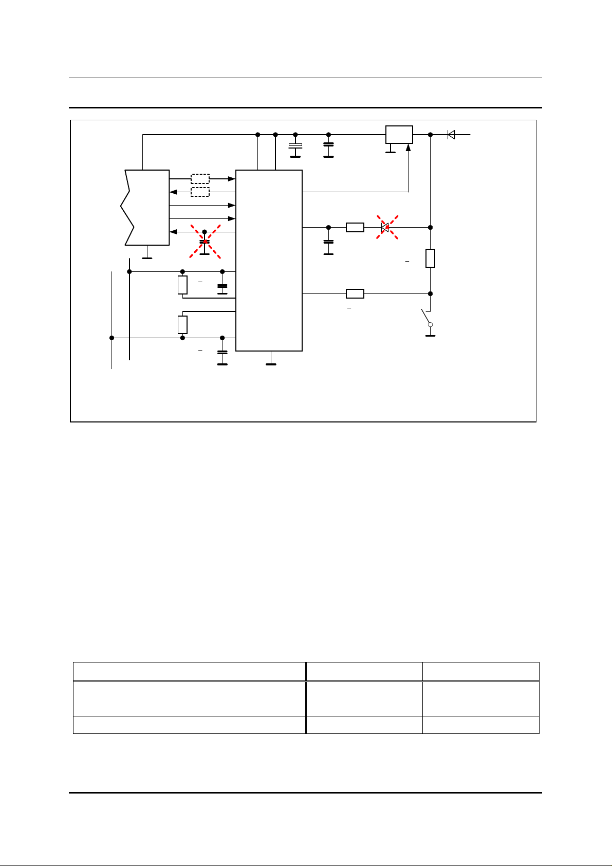
2.2.1. External Components
When the TJA1053 is replaced by a TJA1054, t wo external hardware c omponents ma y be removed
(see also figure 1) :
•
Reverse current protection diode at pin BAT
•
Pulse lengthening capacitor at pin ERR
The extra diode for th e TJA1053 is needed to suppress a rever se power suppl y of the contro l unit if
the battery connection of the e ntire unit was lost. For the TJA1053, a c urrent flow f rom the CANL bus
line backward to the pin BAT of the transceiver was pos sible if the transceiver was not powered. In
some applications, this re verse current was high enough to s upply the m icrocontroller un intentionall y.
The TJA1054 is internally protected against such reverse currents making the diode superfluous.
Reading the pin ERR during the normal CAN interrupt service routine was not possible for the
TJA1053 in case of “ open f ailures ” on t he bus l ines . Here, the so- called “ ack nowledge bi t” of an y valid
CAN message cleared an already detected “open failure” at the pin ERR. Therefore, an external
lengthening capacit or was required for the TJ A1053 in order to keep t he detected failure signa l valid
until the interrupt service routine was executed by the host uC.
The TJA1054 does not require this extr a len gth eni ng c a pacitor since the pin E RR no w i nternally keeps
the failure signal active. ( see also 11.2.1. )
Application Hints V3.1 Page 7 of 41
Page 8
Philips Semiconductors Systems Laboratory Hamburg, Germany
APPLICATION HINTS Fault-tolerant CAN Transceiver
100n
**
VCC
TXD TXD
RXD RXD
uC
I/O STB
+
CAN
GND
RTH***
RTL***
CAN
bus
* For further EMC optimization a series resistor could be applied in case the bus timing parameters allow this additional delay
caused by the additional R/C time constant.
** Size of capacitor depends on regulator.
*** Size of termination resistors depends on system size. The overall system termination should be about 100 Ohms per CAN line.
optional *
<150pF
<150pF
ERRI/O
470n
CANH
RTH
RTL
CANL
ENI/O
PCA82C252
V
or
TJA1053
or
TJA1054
GND
CC
INH
V
BAT
WAKE
1k - 2k
10n
> 1k8
5V
<180k
WAKE-UP
BAT
Figure 1 : Typical application circuitry using the TJA1053 and the TJA1054
2.2.2. Wake-up sensitivity at pin WAKE
The wake-up input of the TJ A1054 is s ensitiv e on bo th edg es, whereas the T JA1053 was s ensit ive on
the falling edge only. This has typically no impact on the application since such external wake-up
events are usually pulses including both edges.
Another improvem ent of the TJ A1054 is that wak e-up events have higher pr iority than the goto-sle ep
command. System s using the TJA1053 may lose such a wake-up event. Consequent ly, a TJA1053
node may keep sleeping without starti ng the voltage regu lator although a wake- up request has been
driven to the pin W AKE. The TJ A1054 will now reco gnise any wak e-up event independentl y from the
current command setting of the host CPU.
2.2.3. Current consumption
The total current cons um ption of the TJ A1054 is reduc ed c om pared to t he T JA1053 , es pec iall y durin g
low-power modes. The slightly increased short circuit current of the CANH bus driver within the
TJA1054 is compensated by its reduced normal mode supply current during dominant bus states.
Thus, there is no im pact to the applications power s upply concept. But introduction of the TJA1054
provides a much lower sleep current per control unit now compared with the TJA1053.
Condition TJA1053 TJA1054
Current consumption in Normal Mode, I
CC
Current consumption in Low-power Modes, I
BAT + ICC
6 mA recessive
29mA dominant
7 mA recessive
17mA dominant
70uA 30uA
2.2.4. Operating Voltage Range
In order to increase the system perf ormance during low battery conditions, the T JA1054 now allows
operation down to 5V at the pin BAT, whereas the TJA1053 required at least 6V.
Application Hints V3.1 Page 8 of 41
Page 9

Philips Semiconductors Systems Laboratory Hamburg, Germany
APPLICATION HINTS Fault-tolerant CAN Transceiver
2.3. Software Issues
2.3.1. Error signalling via pin ERR
As already mention ed before, the behavi our of the error signa lling at the pin ERR is im proved within
the TJA1054. This al lows removing the ext ernal lengthening capacitor needed for the T JA1053 (see
also 2.1). This new behaviour of the TJA1054 may have an impact on application software if the
TJA1053 was used
2.3.1.1. Software polls pin ERR
Application software polling the pin ERR will see fewer transitions if th e TJA1053 is replaced b y the
TJA1054. Especiall y during “open failures” on th e bus lines , the soft ware load cause d by ERR eve nts
is reduced if the TJA1054 is used.
2.3.1.2.Software reads pin ERR during CAN interrupt service only
Here, the “open failures” are now detected
TJA1053 has signal led no problem. Thus , a s im ple migration to the TJ A105 4 a utomatically im proves a
software driven diagnosis function.
2.3.2. VCC Standby / PWON Standby
The VCC Standby Mode k nown f rom the T JA1053 is replaced b y the so-c alled PWO N Standb y Mode
in the TJA1054 (STB = 1; EN = 0). There is no change in functionality between both transceivers
except for the CANL biasing level. The TJA1053 drives 5V to CANL through pin RTL and the
termination resistor, whi le the TJA1054 now drives 12V to CAN L using the same path. This has no
impact on the overall system performance if both transceivers are m ixed in one network. Software is
not influenced since both transc eivers provide the same status inf ormation to the microcontr oller via
ERR and RXD.
without
external lengthening capacitor. Two scenarios are possible:
and
signalled by the TJA1054 as desired, whereas the
2.3.3. First Battery Connection, behaviour of pin INH
The TJA1053 allows to be s et into Sleep Mode ( INH floating) direc tly after first batter y connection by
driving the goto-sleep com mand to the control pins ST B and EN (“01”) . The TJ A1054 needs t o be set
into Normal Mode bef ore accepting the first go to-sleep command af ter first connectio n of the batter y
supply. After setting Normal Mode both devices behave identical concerning this item.
An internal power-on reset signal within the TJA1054 makes sure that the transceiver is reset
successfully after power- up and the INH output is saf ely set to batter y level. This internal reset si gnal
is cleared whenever the Norm al Mode is entered once. There are no special timing requir ements to
clear the internal reset sig nal thus sof tware just has to se t the Norm al Mode via STB a nd EN fol lowed
by any other control cod e. Within mos t of the existing app lications this is already implem ented inside
of the systems cold-start routines.
2.3.4. Goto-Sleep / Wake-up Priority
The pin INH of the TJ A1053 does ignore wak e-up events in case these wake-up events are present
while the goto-sleep command is continuously driven to t he tr a ns c ei ver vi a pi ns STB and EN ( ST B = 0
/ EN = 1). After the goto-sleep filter tim e ( see dat a shee ts T JA1054/T JA10 54A : “ react ion tim e of goto
sleep command” ) the INH flip-flop is continuously cleared thus setting the pin INH to a floating
condition. Wak e-up events are forwar ded to INH first with releasing the goto- sleep comm and. Thus a
systems voltage regu lator connected to INH will becom e disabled e ven if there is a pend ing wake-up
request. Nevertheless RXD and ERR will signal the wake-up event with a LOW output level
independently from the pending goto-sleep command.
For the TJA1054 this behaviour is improved and no wake-up event is lost with respec t to the pin INH.
Within the TJA1054 the wake-up events ha ve a higher priority than the goto-sl eep command. Thus
any wake-up event will reset IN H to a HIG H out put le vel i ndepen dentl y from the goto-s leep c omm and.
RXD and ERR will reflect the wake-up condition with a LOW output level as known from the TJA1053.
From software point of view it is highl y recommended for both transc eivers monitoring the pi ns RXD
and/or ERR whenever the goto-sleep command was executed in order to detect a wake-up event
Application Hints V3.1 Page 9 of 41
Page 10

Philips Semiconductors Systems Laboratory Hamburg, Germany
APPLICATION HINTS Fault-tolerant CAN Transceiver
while the system s hould f all in to s l eep mode. INH might keep HIG H or become HIG H ag ai n c aus e d by
a wake-up event before the supply of the uC was successfully disabled. ( see also 11.1. )
2.3.5. Other issues
Experiences with dif ferent software drivers have sho wn the advantage to implement a kind of CAN
communication m onitoring in software, expecting CAN b us events in certain time fr ames. At least a
reception of mes sages or succ essful transm issions should appear in or der to get conf idence, th at the
CAN bus is still operating properly. This is especially important for recovery from dual bus failure
situations towards single bus failure situations.
Due to the automatic transmit message repetition mechanism of a CAN protocol engine it might
happen that a node r etransm its a message forever in case t here is no ack nowledge rec eived fr om the
bus. This continuously transm itting node might lock the bus system and thus prevents other nodes to
recover from a dual bus failure situation towards a single bus failure situation.
Therefore, whenever there is no response from the CAN bus within a reasonable time, pending
transmission requests should be abor ted in software. This will inc rease the system avai lability during
certain bus failure conditions, which require single wire operation.
2.4. Interoperability : Mixed Systems with TJA1053 and TJA1054
2.4.1. Overview
During developm ent of the TJA1054 special attention was paid to interop erability issues in order to
allow a smooth m igration of existi ng applicatio ns by simple replacement of the T JA1053. Part icularly,
the enhancements of the bus f ai lure management (5V s hor t cir cuits) have been included very car ef ul l y
into the existing circuitry to avoid system hang-ups, if both transceivers are mixed in one system.
The TJA1054 is designed to replace the TJA1053 within running car series production without
interoperability risk.
Interoperability of both devices has been proved in system simulation as well as in hardware
investigation.
The key results of these investigations are :
•
A pure TJA1054 network solves the known weaknesses of a TJA1053 system
( wake-up of big networks with failure HxGND, short circuits to 5V .... )
•
A mixed system of TJA1053 and TJA1054 has at least the same performance as the pure
TJA1053 system; in some aspects the growing presence of T J A1054 no des i n th e n et work even
improves the overall system performance
•
T aking into consi deration the is sues desc ribed in the previous cha pters, m ixed systems of both
transceiver are possible at any ratio without restrictions
2.4.2. Hardware Interoperability Investigations
In order to investigate in teroperability issues of th e transceiver, a network with 25 nodes was set up
and investigated in detail. A typical topology including star points was chosen according to real
automotive applicat ions. This topology inc ludes cable stubs with m ore than 5 meters and more than
55 meters overall cable length.
Worst case scenarios were analysed including weak bus failure conditions, double failures, ground
shifts and power sup ply drops. Esp ecially, oper ating mode c hanges (Norm al Mode / Sta ndby / Sleep)
were performed simultaneously with bus failure situations.
Application Hints V3.1 Page 10 of 41
Page 11
Philips Semiconductors Systems Laboratory Hamburg, Germany
APPLICATION HINTS Fault-tolerant CAN Transceiver
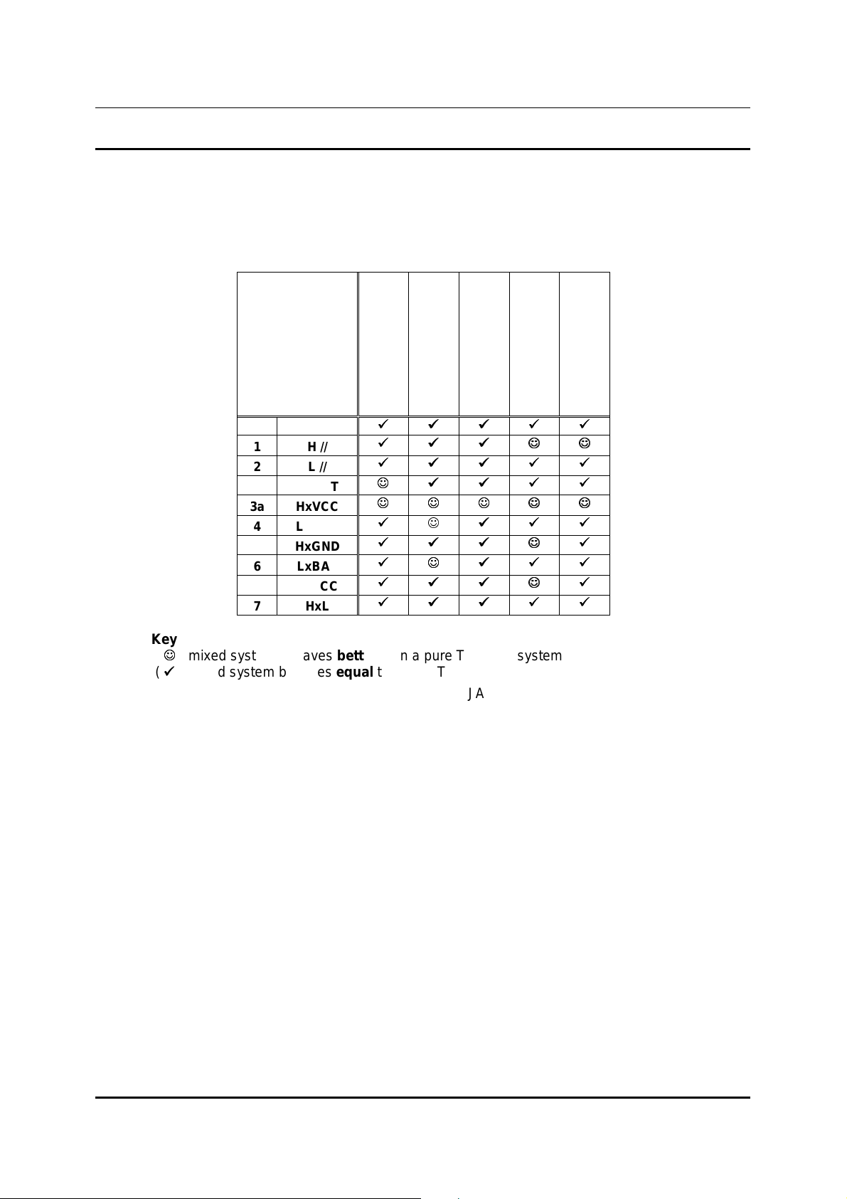
2.4.3. Results of Hardware Interoperability Investigation
The following table gives an overview about the mixed system investigations using the TJA1053
together with the TJA10 54 in different mixing ratios. An assessment is made compar ed with a pure
TJA1053 system with same topology.
Bus Failure
0 none
1 H //
2 L //
3HxBAT
3a HxVCC
4LxGND
5HxGND
6LxBAT
6a LxVCC
7HxL
9
9
9
9
9
9
-
-
-
-
9
9
9
9
9
9
9
9
9
9
Communication with
( incl. resistive failures )
Standard Communication
9
9
9
9
9
9
9
9
-
-
-
9
9
-
-
9
9
9
9
Communication at
9
9
9
9
9
9
9
9
-
-
9
9
9
9
9
9
9
9
9
9
Low Battery Voltages
Ground Shift (+/- 1.5V)
combined with Bus
Mode Changes / Wake-up
9
9
-
-
9
9
9
9
-
-
9
9
-
-
9
9
-
-
9
9
Failure Conditions
9
9
-
-
9
9
9
9
-
-
9
9
9
9
9
9
9
9
9
9
Loss of Termination
Communication with local
Key :
(
-- ) mixed system behaves
(
99 ) mixed system behaves
'
) mixed system behaves
(
than a pure TJA1053 system
better
to a pure TJA1053 system
equal
worse
than a pure TJA1053 system
2.5. Conclusion
Both transceivers, T JA1053 and TJA1054, are in teroperable and can be us ed simultaneously within
the same network. This allows migrating gradually from TJA1053 to TJA1054 in running car mass
production.
Due to new features intr oduc ed wit h the T JA1054, exis ting T JA10 53 a pplicat ions nee d to be r eview ed
according to the comments within this report before replacing the transceiver.
Application Hints V3.1 Page 11 of 41
Page 12

Philips Semiconductors Systems Laboratory Hamburg, Germany
APPLICATION HINTS Fault-tolerant CAN Transceiver
2.6. Migration Checklist
Item TJA1053 TJA1054 Comment
Diode @ pin BAT needed can be removed no reverse power supplying by
TJA1054
Capacitor @ pin ERR depends on
software
Sensitivity of pin WAKE falling edge only both edges check behaviour of system wake-up
Goto-sleep command
after first battery
connection
Goto-sleep command,
priority of wake-up event
always possible possible only after
INH becomes
floating the time
goto-sleep is driven
even if there is a
wake-up coming
can be removed function is integrated into the
TJA1054
via pin WAKE
Internal power-on signal has to be
Normal Mode was
entered once
INH keeps HIGH if
there is a wake-up
coming during gotosleep is driven
cleared by setting the TJA1054 into
Normal Mode after first battery
connection
It is recommended to monitor pin
RXD and/or pin ERR after goto-
sleep in order to detect a wake-up
event during the transition into
Sleep Mode.
Application Hints V3.1 Page 12 of 41
Page 13
Philips Semiconductors Systems Laboratory Hamburg, Germany
APPLICATION HINTS Fault-tolerant CAN Transceiver
3. Mode Control with the TJA1054
3.1. Overview
The fault tolerant CA N trans c eiv er T J A1054 provides an integrated functi ona lity controlling an external
voltage regulator in order to design low power CAN bus systems with remote and local wake-up
capabilities. A dedicated INH pin allows disabling the entire power supply of a control unit, thus
reducing the overall system power consumption to a m inimum. The transceiver is the only supplied
component during such a low-power state.
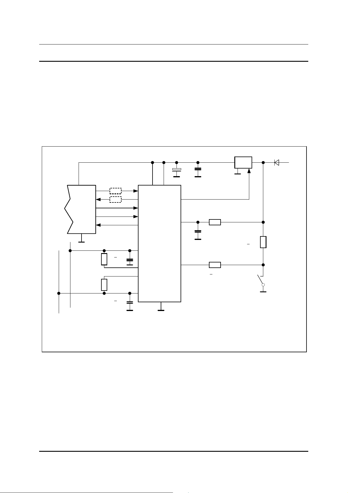
Following figure shows an application example using the TJA1054.
**
VCC
TXD TXD
RXD RXD
uC
I/O STB
+
CAN
GND
RTH***
RTL***
CAN
bus
* For further EMC optimization a series resistor could be applied in case the bus timing parameters allow this additional delay
caused by the additional R/C time constant.
** Size of capacitor depends on regulator.
*** Size of termination resistors depends on system size. The overall system termination should be about 100 Ohms per CAN line.
optional *
ENI/O
ERRI/O
CANH
<150pF
RTH
RTL
CANL
<150pF
V
TJA1054
GND
CC
INH
V
BAT
WAKE
100n
1k - 2k
10n
> 1k8
5V
<180k
WAKE-UP
BAT
Figure 2 : Typical application of the TJA1054
As shown within Figure 2 the transceiver is powered d irectly from the battery s upply via the pin BAT.
This allows disabling the VCC supply entirely during tim e phases, the CAN bus is not required b y the
system. Therefore two control pins STB and EN coming from the host microcontroller are used to
control the actual mode of operation like normal communication or low-power operation.
For wake-up purposes a battery-related WAKE pin is provided.
In addition to bus fail ure information and the CAN receive d bit stream, the pins ERR and RXD are
used to signal wake-up requests towards the application controller.
Application Hints V3.1 Page 13 of 41
Page 14

Philips Semiconductors Systems Laboratory Hamburg, Germany
APPLICATION HINTS Fault-tolerant CAN Transceiver
3.2. Operating Modes
The two fail-safe coded pins STB and EN mainly control the power management of the TJA1054.
They are defining directly the actual mode of operation as illustrated within Figure 3.
The following operating modes are implemented:
•
Normal Mode normal transceiver operation
•
Goto Sleep disables the external voltage regulator via INH after a certain time out
•
Stby Sleep similar to Goto Sleep, but INH is not affected
•
PWON Stby similar to Stby Sleep, but allows to read back the PWON flag
indicating a power-on condition
All modes different from Normal Mode are low-power modes reducing the current consumption
significantly.
o
P
CC (stb)
n
r O
e
w
(NSTB = 0
OR
AND
EN = 0)
Power Fail
NSTB = 0
AND
EN = 1
Goto
Sleep
(NSTB = 0
Power Fail
OR
AND
(NSTB = 1
(NSTB = 0
AND
EN = 0)
AND
EN = 1)
(NSTB = 1
(NSTB = 0
EN = 1)
Power ok
Normal
AND
EN = 0)
AND
EN = 1)
AND
(NSTB = 0
OR
Stby
Sleep
(NSTB = 1
AND
EN = 1)
EN = 0)
Power Fail
(NSTB = 1
Power On
AND
NSTB = 1
EN = 0
AND
AND
Pwon
Stby
AND
EN = 0)
Power ok
(NSTB = 1
AND
EN = 1)
AND
Power ok
Fail
VCC > V
CC (stb)
OK
Power Fail
VCC < V
Figure 3 : Operating Modes of the TJA1054
Note, that a change from the power-on condition (STB and EN = “0”) is possible only, if the VCC
supply is present. Whenever VCC fa lls b el o w a c ertai n leve l ( s e e da ta s he et TJA1054: “supp ly voltage
for forced Standby Mode” ) the fail-saf e Stand b y Mode is ent ered automatically (power-fai l).
Depending on the selected mode of operation, the I/O pins provide different information for the
application as described within the next chapters.
3.2.1. Normal Mode
During normal mode the transceiver is used to transmit data to the bus and to receive dat a from the
CAN bus. Here the pin RXD reflects the bus signal and the pin ERR is used to signal bus failure
conditions with an active LOW behaviour.
Application Hints V3.1 Page 14 of 41
Page 15

Philips Semiconductors Systems Laboratory Hamburg, Germany
APPLICATION HINTS Fault-tolerant CAN Transceiver
3.2.2. Goto Sleep
Entering Goto Sleep the transce iver immediatel y changes int o low-power o peration, while the pin I NH
is still kept active HIGH. N ow a n intern al wak e- up flip-f lop is output via t he pins RXD and ERR , if VC C
is present. Thus both pin’s signa ls can b e use d to wak e- up the ap plicati on with an ac ti ve low sign al. If
the Goto Sleep state k eeps present for a certain time ( see data sheet TJA1054: “reaction tim e of
goto-sleep command” ) the INH output of the TJA1054 becomes “floating” disabling the externally
connected voltage regulat or. The application can keep within the Got o Sleep state or switch over t o
Stby Sleep mode without any difference in behaviour of the transceiver.
Typically the applicatio n automatically changes towar ds Stby Sleep because the power supply of the
host microcontroller becom es disabled during Got o Sleep and thus the c ontrol pins STB and E N are
falling towards a LOW signal with the decreasing supply of the microcontroller.
3.2.3. Stby Sleep
If the system needs to k eep the external voltage reg ulator active for some r eason during low-power
operation, this m ode c an be en ter ed direc t l y from normal mode. Then the pin INH keeps HIGH all time
and the external voltage regulator stays alive. During this mode RXD and ERR are signalling a
possible wake-up condition as described for the Goto Sleep state.
The internal “sub-modes” Standby and Sleep are distinguished only by the state of the pin INH. In
case of a previous successful Goto Sleep procedure INH is floating during Stby Sleep.
3.2.4. PWON Stby
This mode behaves similar to Stb y Sleep with the diff erence that th e pin ERR allows re ading bac k the
internal PWO N flag. This flag is set whe never the transce iver is powered with battery suppl y the first
time. So the applicat ion can disti nguish between a cold start situat ion caused b y a system sleep or a
cold start due to first battery connection of the device.
3.3. System Wake-up
Once the transceiver is not within Normal Mode there are th e following possibilities to wak e-up the
system:
•
Local wake-up using the local pin WAKE
•
Remote wake-up caused by CAN bus traffic
•
Mode change entering Normal Mode via STB and EN
3.3.1. Local wake-up
A local wake-up can be forced with an edge at t he pin WAKE of the transc eiver. A positive edge as
well as a negative edge r esults in a system wake-up if the signal keeps constant f or a certain time
(see data sheet TJA1054: “required time on pin WAKE for local wake-up”). Thus short spikes are
filtered and do not result in unwanted system wake-up conditions.
As a result of the edge at pin WAKE, the intern al wak e-up flip- flop is s et and outp ut at ER R and RXD .
Additionally the pin INH becomes HIGH again, starting the external voltage regulator.
Note that the pin WAKE provides an inter nal weak pull-up curr ent towar ds batter y in order to pro vide a
defined condition in case of open circuit.
3.3.2. Remote wake-up
Another possibility waking u p the system is traffic on the CAN bus lines. Whenev er the bus becom es
dominant for a certain time within a CAN message (see data sheet TJA1054: “dominant time for
remote wake-up on pin C ANH or CANL” ) the int erna l wak e-up fli p-flop is set and the pin INH activ ates
the external voltage regulator.
3.3.3. Mode change
The connected host m icrocontroller can directly switch the transceiver into Normal Mode by setting
STB and EN High in case the VCC supply is present at the transceiver.
Application Hints V3.1 Page 15 of 41
Page 16

Philips Semiconductors Systems Laboratory Hamburg, Germany
APPLICATION HINTS Fault-tolerant CAN Transceiver
3.4. State diagrams
Within this chapter some state diagram s are collec ted showin g the behav iour of the T JA1054 in m ore
detail.
3.4.1. PWON Flag
The PWON flag is set whenever the transceiv er is supplied the f irst time or the batter y voltage drops
below a certain lim it (s ee data sheet T JA1054: “pow er-on f lag vo ltage on pin BAT ”). It is c leared when
entering the Normal Mode.
3.4.2. Pin INH
The pin INH is controlle d b y the Goto S leep s tate a nd the wak e-up events . Ther e is a prior ity of wakeup in order to make sure that any wake-up event keeps the external voltage regulator active
independently of a goto-sleep command.
Note that a successful Goto Sleep is possible only if the Normal Mode was entered once after a
power-on condition. The PWON flag has to be cleared making sure that the system was started
successfully before entering the Sleep Mode the first time.
3.4.3. Wake-up Flag
An internal wak e-up flag is set upon a local or rem ote wake-up event. This flag is cleared whenever
the Normal Mode is en tered via STB and EN. The content of this flag is signalled v ia RXD and ERR
according to the corresponding state diagrams.
n
r O
e
w
o
P
n
r O
e
w
o
P
VBAT
Clear
n
er O
w
o
P
Set
Normal Mode
V
Clear
PWON Flag
(Goto Sleep) > t
No Wake-up Event
< V
BAT
BAT (pof)
NOT
AND
AND
PWON
r (SLEEP)
[ (BUS = dominant) > t
NOT
Change @ NWAKE > t
(STB = 1
AND
Float
Pin INH
Figure 4 : State Diagrams, PWON Flag, pin INH and Wake-up Flag
AND
Normal ]
OR
OR
V
CC
CAN
WAKE
> V
)
CC (stb)
[
Normal
NOT
AND
(BUS = dominant) > t
OR
Change @ NWAKE > t
CAN
WAKE
]
Normal
Set
Wake-up Flag
3.4.4. Pin RXD
During Normal Mode t he p in RXD r ef lects the ac tua l b us signal. Immediately with c h ang ing in to o ne of
the low power modes, the content of the internal Wake-up Flag is reflected at pin RXD if the VCC
supply of the transceiver is present. A wake-up condition is signalled active LOW.
Application Hints V3.1 Page 16 of 41
Page 17

Philips Semiconductors Systems Laboratory Hamburg, Germany
APPLICATION HINTS Fault-tolerant CAN Transceiver
3.4.5. Pin ERR
The pin ERR is used to signal bus failure conditions during normal operation with an active LOW
behaviour. As soon as the transceiver is switched into Goto Sleep or Stb y Sleep Mode the inter nal
Wake-up Flag is ref lect ed vi a E RR s imilar to the pi n RX D. A change towards PW ON Stby immediatel y
switches ERR to the in ternal PW ON Flag. A power -on conditio n is signa lled acti ve LOW . Please take
care that the external loading to the pin ERR may cause a delay changing the level from LOW to
HIGH. Typically a uC-por t pin caus es a lo ad of s ome 10pF to th e pin ERR. Due to th e re lativel y weak
pull-up behaviour of the pin ERR, charg in g this wire may need relev ant t ime for fast operat ing s of t ware
( see also 11.3. ).
Bus
Goto Sleep
OR
Stby / Sleep
OR
PWON Stby
Bus
Signal
Wake-up
Flag
Normal
Goto Sleep
OR
Stby / Sleep
Wake-up
Flag
P
ow
er O
n
Power On
Failure
Normal
Goto Sleep
OR
Stby / Sleep
PWON Stby
Normal
PWON Stby
PWON
Flag
Pin RXD
Pin ERR
Figure 5 : State Diagrams, pins RXD and ERR
Application Hints V3.1 Page 17 of 41
Page 18

Philips Semiconductors Systems Laboratory Hamburg, Germany
APPLICATION HINTS Fault-tolerant CAN Transceiver
4. Vcc Supply and Recommended Bypass Capacitance
4.1. List of used Abbreviations
Table 4-1 : Used abbreviations
Symbol Description
I
cc_dom
I
cc0_dom
I
CANH_dom
I
RTL_dom
I
cc_rec
I
cc_norm_avg
I
cc_sc1_dom
I
CANH_sc1_dom
I
cc_sc1_avg
∆
I
cc_sc1
I
cc_sc2_dom
I
RTL_sc_dom
∆
I
cc_sc2
V
CC
V
CANL_dom
R
T
t
dom_max
∆
V
max
C
BUFF
Supply current at pin VCC while driving a dominant bit
Supply current at pin VCC while driving a dominant bit
Output current of pin C ANH whi le dri ving a dom inant bit with n om inal bus load of 100
Ohms in total
Output current of pin RTL while driving a dominant bit with a certain load
Supply current at pin VCC while driving a recessive bit
Average supply current at pin VCC assuming no bus failure and continuous sending
Supply current at pin VCC driving a dominant bit while CANH is shorted to GND
Output current of pin CANH driving a dominant bit while CANH is shorted to GND
Average supply current at pin VCC assum ing CANH shorted to GND and cont inuous
sending
Supply current change at pin VCC in case a dominant bit is driven while CANH is
shorted to GND
Supply current at pin VCC drivi ng a dom inant bit whi le CANH
to GND
Output current of pin RTL while driving a dominant bit with CANL shorted to GND
Supply current change at pin VCC in case a dom inant bit is driven whil e CANH and
CANL are shorted to GND
Supply voltage at pin VCC
Voltage level on CANL while a dominant bit is driven
Termination resistor connected to pins RTL and RTH
Maximum possible continuous dominant drive time
Maximum allowed voltage change at pin VCC
Required buffer capacitance in case the voltage regulator does not deliver extra
current within t
dom_max
with
a certain load to the pins
without
any load to the pins
and
CANL are shorted
Application Hints V3.1 Page 18 of 41
Page 19

Philips Semiconductors Systems Laboratory Hamburg, Germany
APPLICATION HINTS Fault-tolerant CAN Transceiver
4.2. Summary
In order to properly dimension the Vcc s upply of the fault-tolerant CAN tr ansceivers two parameters
have to be taken into account:
1) the average supply current
2) the peak supply current
The average supply current is needed to calculate the thermal load of the required Vcc voltage
regulator. The peak supply curr ent ma y flow in case of certain bus failur e conditi ons f or a c ertain t ime
and thus has an impact on the power supply buffering.
The Vcc supply of the transceiver is recommended to support the characteristics as follows:
Table 4-2 : Overview of supply currents
Item PCA82C252 TJA1053 TJA1054
Average Vcc supply current without bus failures 44.5 mA 44.5 mA 41 mA
Average Vcc supply current at presence of
single bus failures
Worst case peak Vcc supply current at presence
of single bus failure (for 6 bit times max.)
Worst case peak Vcc supply current at presence
of dual bus failures (for 17 bit times max.)
74.5 mA 74.5 mA 76 mA
139 mA 139 mA 141 mA
140 mA 140 mA 142 mA
The capacitive buff ering needed for the transcei ver depends on the system s power concept and the
regulator characteristic of the used voltage regulator chip.
In case the transceiv er has a
supply current dur ing single bus fail ures is relevant because here th e communic ation medium has to
keep unaffected. T he worst case dual failure situation is not relevant since here the c ommunication
medium is complete ly out of operation and the transceiver does not need to be supplied anymore.
Such systems ar e recommended to pr ovide a bypass capacitanc e of
wiring faults.
regulation time constant is fast enough.
In case the transceiver’s Vcc power supply is
current during the worst case dual failur e situation has to be tak en into account. This is b ecause the
uC has to keep a proper supply even if there is no CAN comm unication pos sible at all. Such s ystems
are recommended to provide a bypass capacitance of
behaviour this capacitan ce may become much smaller if the regulation time constant is fast
enough.
This capacitance can be implemented as a separate component or alternatively through a
corresponding increas e of the capacitance of the b ypass capacitor being locat ed at the Vcc vo ltage
regulator.
In the following, relevant cases are considered in more detail.
Depending on the regulator behaviour this capacitance may become smaller if the
separated
Vcc power suppl y apart from the microcontroller, the peak
shared
47 uF
with its host microcontroller, the peak supply
150uF. Depending on the regulator
in order to support s ingle
Application Hints V3.1 Page 19 of 41
Page 20

Philips Semiconductors Systems Laboratory Hamburg, Germany
APPLICATION HINTS Fault-tolerant CAN Transceiver
4.3. Average Supply Current at Absence of Bus Short-Circuit Conditions
In recessive state the different transceivers are consuming a Vcc supply current as listed in the
corresponding data s heets. In dominant state t he Vcc supply current is calculated by the addition of
the IC-internal supply current ( see data she et TJA105 4: “no lo ad” condit ion) an d the output current a t
pins CANH and RTL.
4.3.1. Maximum dominant supply current (without bus wiring faults)
I
cc_dom
I
RTL_dom
= I
cc0_dom
= (Vcc - V
+ I
CANH_dom
CANL_dom
+ I
) / R
RTL_dom
T
(1)
(2)
4.3.1.1.Example calculation
Maximum dominant supply current without bus wiring faults:
Item from Data Sheet / Assumptions Symbol PCA82C252 TJA1053 TJA1054
Max. Vcc supply current dominant, no load
CANH dominant current
Assumed termination resistor
Assumed CANL dominant voltage
PCA82C252
TJA1053
TJA1054
: I
: I
: I
cc_dom 252
cc_dom 1053
cc_dom 1054
= 35mA + 40 mA + (5V - 1V) / 1k = 79 mA max. (Ex 1.1)
= 35mA + 40 mA + (5V - 1V) / 1k = 79 mA max. (Ex 1.2)
= 27mA + 40 mA + (5V - 1V) / 1k = 71 mA max. (Ex 1.3)
I
cc0_dom
I
CANH_dom
R
T
V
CANL_dom
35 mA 35 mA 27 mA
40 mA 40 mA 40 mA
1 k 1 k 1 k
1 V 1 V 1 V
4.3.2. Thermal considerations (without bus wiring faults)
For thermal consider ations the average sup ply current at pi n Vcc is relevan t considering the tra nsmit
duty cycle. In the f ollowing exam ple a continuousl y transmitting n ode is as sumed. T his might h appen
e.g. if a node starts a transmission while the rest of the network does not respond with an
acknowledge for s ome reason. Typically a m uch lower duty cycle is relevant since a node transm its
messages within certain time slots only, depending on the applications network management.
With an assumed transmit duty cycle of 50% on pin TxD, the maximum average supply current is
I
cc_norm_avg
= 0.5 * (I
cc_rec
+ I
cc_dom
) (3)
4.3.2.1.Example calculation
Thermal considerations without bus wiring faults:
Item Symbol PCA82C252 TJA1053 TJA1054
Vcc supply current recessive, max.
PCA82C252
TJA1053
TJA1054
:I
cc_norm_avg 252
:I
:I
cc_norm_avg 1053
cc_norm_avg 1054
= 0.5 * (10mA + 79mA) =
= 0.5 * (10mA + 79mA) =
= 0.5 * (11mA + 71mA) =
I
cc_rec
10 mA 10 mA 11 mA
44.5 mA max.
44.5 mA max.
41 mA max
. (Ex 3.3)
(Ex 3.1)
(Ex 3.2)
Application Hints V3.1 Page 20 of 41
Page 21

Philips Semiconductors Systems Laboratory Hamburg, Germany
APPLICATION HINTS Fault-tolerant CAN Transceiver
4.4. Average Supply Current at Presence of a Short-Circuit of one Bus Wire
The maximum Vcc supply current occurs with a bus wire s hor t-c irc uit bet wee n CANH and GND. In this
case the CANH outputs a maximum short circuit current in dominant state (see data sheets). For
thermal considerations the average supply current is relevant. For buffering considerations the
maximum dominant supply current is relevant.
4.4.1. Maximum dominant supply current (with CANH shorte d to GND)
I
cc_sc1_dom
= I
cc0_dom
+ I
CANH_ sc1_dom
+ I
RTL_dom
( t < 6 bit times ) (4)
The 6-bit time limitation is caused by a supposed Error Flag to be sent by the CAN Controller.
4.4.1.1.Example calculation
Maximum dominant supply current with CANH shorted to GND:
Item Symbol PCA82C252 TJA1053 TJA1054
CANH dominant current, short circuit I
PCA82C252
TJA1053
TJA1054
: I
: I
: I
cc_sc1_dom 252
cc_sc1_dom 1053
cc_sc1_dom 1054
= 35mA + 100 mA + (5V - 1V) / 1k =
= 35mA + 100 mA + (5V - 1V) / 1k =
= 27mA + 110 mA + (5V - 1V) / 1k =
CANH_sc1_dom
100 mA 100 mA 110 mA
139 mA max.
139 mA max.
141 mA max.
(Ex 4.1)
(Ex 4.2)
(Ex 4.3)
4.4.2. Thermal considerations (with CANH shorted to GND)
For thermal consider ations the average sup ply current at pi n Vcc is relevan t considering the tra nsmit
duty cycle. With a transmit duty cycle of 50% on pin TxD, the maximum average supply current at
CANH to GND short-circuit is:
I
cc_sc1_avg
= 0.5 * (I
cc_rec
+ I
cc_sc1_dom
) (5)
4.4.2.1.Example calculation
Thermal considerations with CANH shorted to GND:
PCA82C252
TJA1053
TJA1054
: I
: I
: I
cc_sc1_avg 252
cc_sc1_avg 1053
cc_sc1_avg 1054
= 0.5 * (10mA + 139mA) =
= 0.5 * (10mA + 139mA) =
= 0.5 * (11mA + 141mA) =
74.5 mA max.
74.5 mA max.
76 mA max.
(Ex 5.1)
(Ex 5.2)
(Ex 5.3)
Application Hints V3.1 Page 21 of 41
Page 22

Philips Semiconductors Systems Laboratory Hamburg, Germany
APPLICATION HINTS Fault-tolerant CAN Transceiver
4.4.3. Vcc extra supply current in single fault condition
Compared to the quiescent current in recessive state the maximum
CANH driver is turned on with CANH shorted t o GND is needed to c alculate the required worst case
Vcc buffer capacitance. This ex tra supply current has to be buffered for up to 6 bit times, depending
on the applications voltage regulator.
extra
supply current when the
I
∆
cc_sc1
= I
cc_sc1_dom
- I
(6)
cc_rec
4.4.3.1.Example calculation
Vcc extra supply current in case of single fault condition.
Item Symbol PCA82C252 TJA1053 TJA1054
Min Vcc supply current, recessive I
1) The minimum quiescent current is estimated since this value is not specified for the PCA82C252 and the TJA1053.
PCA82C252
TJA1053
TJA1054
:
:
: ∆ I
∆
∆
cc_sc1 252
I
cc_sc1 1053
I
cc_sc1 1054
= 139 mA - 3.5 mA =
= 139 mA - 3.5 mA =
= 141 mA - 4 mA =
cc_rec
3,5 mA
135.5 mA max.
135.5 mA max.
137 mA max.
1)
3,5 mA
1)
4 mA
(Ex 6.1)
(Ex 6.2)
(Ex 6.3)
Application Hints V3.1 Page 22 of 41
Page 23

Philips Semiconductors Systems Laboratory Hamburg, Germany
APPLICATION HINTS Fault-tolerant CAN Transceiver
4.5. Worst Case Max Vcc Supply at Presence of a Dual Short Circuit
The worst case m ax. Vcc supply current is flowing in case of a
CAN_H and CAN_L to ground. In this case no communication is possible. Nevertheless the
application suppl y should be able to deliver a proper Vcc f or the microcontroller in order to pre vent
faulty operation.
If there is a
be taken on this dual short circuit cond ition since the transceivers are beha ving fail safe in case of
under voltage conditions and the uC is still powered properly by its own supply.
In case of a
relevant to dimension the required buffer capacitor.
separate
shared
voltage regu lator avai lable supp lying th e transce iver exclus ively,
voltage supply of transceiver and microcontroller this dual fault condition is
dual short-circuit
of the bus lin es
no care
has to
4.5.1. Max Vcc supply current in worst case dual fault condition
I
cc_sc2_dom
I
RTL_sc_dom
The 17-bit time limitation is ca used by the CAN protocol. Due to the dual fault condition with CANH
and CANL shorted to GND the pin RxD of the transcei ver is con tinuo usly clam ped r ecessiv e (CANL t o
GND forces CANH operation; CANH is clamped recessive).
The moment the CAN controller starts a trans m ission, th is dom inant Star t Of Fram e bit is n ot fed b ack
via RxD and thus forces an err or f lag due to t he bit f ailur e cond ition ( TX Error Count er i ncrem ented b y
8). This first bit of the error flag again is not reflected at RxD a nd forces the next err or flag (TX Err or
Counter + 8).
= I
cc0_dom
= Vcc / R
+ I
CANH_sc1_dom
T
+ I
RTL_sc_dom
( t < 17 bit times ) (7)
(8)
Latest after 17 bit tim es, depending on the TX Error Counter Level befor e starting this transm ission,
the CAN controller reaches the Error Passive limit (128) and stops sending dominant bits. Now a
sequence of 25 recessive bits follows (8 Bit Error Delimiter + 3 Bit Intermission + 8 Bit Suspend
Transmission) and the Vcc current becomes reduced to the recessive one.
From now on only single dom inant bits (Start Of Frame) followed b y 25 recessive b its (Passive Error
Flag + Intermission + Suspend Tr ansmission) are output until the CAN controller enters the Bus Off
State.
So, for dimensionin g the Vc c voltag e sourc e in t his worst c ase du al fai lure sc enario, up to 17 b it t imes
might have to be buff ered by a bypass capac itor dependin g on the regulati on capabilities of the used
voltage supply.
4.5.1.1.Example calculation
Max Vcc supply current in worst case dual fault condition:
PCA82C252
TJA1053
TJA1054
: I
: I
: I
cc_sc2_dom 252
cc_sc2_dom 1053
cc_sc2_dom 1054
= 35 mA + 100 mA + 5V / 1k =
= 35 mA + 100 mA + 5V / 1k =
= 27 mA + 110 mA + 5V / 1k =
140 mA max.
140 mA max.
142 mA max.
(Ex 7.1)
(Ex 7.2)
(Ex 7.3)
Application Hints V3.1 Page 23 of 41
Page 24

Philips Semiconductors Systems Laboratory Hamburg, Germany
APPLICATION HINTS Fault-tolerant CAN Transceiver
4.5.2. Vcc extra supply current in dual fault condition
Compared to the quiescent current in recessive state the maximum
CANH driver is turned on in dual short-c ircuit conditio n is needed to calculate t he requir ed worst case
Vcc buffer capacitance. This extra supply current has to be buffered for that time the applications
voltage regulator needs to react.
extra
supply current when the
I
∆
cc_sc2
= I
cc_sc2_dom
- I
(9)
cc_rec
4.5.2.1.Example calculation
Vcc extra supply current in case of dual fault condition.
Item Symbol PCA82C252 TJA1053 TJA1054
Min Vcc supply current, recessive I
1) The minimum quiescent current is estimated since this value is not specified for the PCA82C252 and the TJA1053.
PCA82C252
TJA1053
TJA1054
:
:
: ∆ I
∆
∆
cc_sc2 252
I
cc_sc2 1053
I
cc_sc2 1054
= 140 mA - 3.5 mA =
= 140 mA - 3.5 mA =
= 142 mA - 4 mA =
cc_rec
3,5 mA
136.5 mA max.
136.5 mA max.
138 mA max.
1)
3,5 mA
1)
4 mA
(Ex 9.1)
(Ex 9.2)
(Ex 9.3)
4.6. Calculation of worst-case bypass capacitor
Depending on the power supply concept, the required wo rst-c ase bypass c apacitor c an be ca lculated.
In case of a
single fault condition
the
separate Vcc
supply for the transceiv er only, the extra supp ly current ∆ I
has to be taken with a maximum of 6 dominant bit times.
in case of
cc_sc
If the transceiver and the host microcontroller are supplied from the same regulator (
supply
), the extra supply current ∆ I
in case of the
cc_sc
dual fault condition
has to be taken with a
shared Vcc
maximum of 17 dominant bit times.
C
= ∆ I
BUFF
The capacitor C
BUFF
maximum dominant output drive t
cc_sc
* t
dom_max
/ ∆V
max
is needed if the voltage regulator is
dom_max
during the dual fault condition.
not
able to deliver any extra current with in t he
(10)
Application Hints V3.1 Page 24 of 41
Page 25

Philips Semiconductors Systems Laboratory Hamburg, Germany
APPLICATION HINTS Fault-tolerant CAN Transceiver
4.6.1. Example calculation, separate supplied transceiver @ 83,33kBit/s
In case of a separate tr ansceiver supply the bypass c apacitance has to be calculate d based on the
single fault condition with CANH shorted to GND. Here the dual fault is not relevant.
Assumption of 83,33 kBit/s : t
Maximum allowed Vcc voltage drop :
PCA82C252
TJA1053
TJA1054
: C
: C
: C
= 135.5 mA * 72 us / 0.25 V =
BUFF 252
BUFF 1053
BUFF 1054
= 135.5 mA * 72 us / 0.25 V =
= 137 mA * 72 us / 0.25 V =
∆
= 6 * 12 us = 72 us
dom_max
= 0.25V
V
max
39 uF
39 uF
39,5 uF
(Ex 10.1)
(Ex 10.2)
(Ex 10.3)
In this example the bypass capacitance to be reserved for the Vcc supply of the transceiver is
recommended to be 39,5 uF minimum at 83,33 kBit/s. It may become smaller, if the used voltage
regulator is able to deliver an extra current within t
dom_max
.
4.6.2. Example calculation, shared supply
In case of a shared sup ply concept the b ypass capacitance has to be calculate d based on the worst
case dual fault condition in order to keep the uC supply stabile:
Assumption of 83,33 kBit/s : t
Maximum allowed Vcc voltage drop :
PCA82C252
TJA1053
TJA1054
: C
: C
: C
= 136.5 mA * 204 us / 0.25 V =
BUFF 252
BUFF 1053
BUFF 1054
= 136.5 mA * 204 us / 0.25 V =
= 138 mA * 204 us / 0.25 V =
∆
= 17 * 12 us = 204 us
dom_max
V
= 0.25V
max
111.4 uF
111.4 uF
113 uF
(Ex 10.1)
(Ex 10.2)
(Ex 10.3)
In this example the bypass capacitance to be reserved for the Vcc supply of the transceiver is
recommended to be 113 uF minimum at 83,33 kBit/s. It may become smaller, if the used voltage
regulator is able to deliver an extra current within t
dom_max
.
Application Hints V3.1 Page 25 of 41
Page 26

Philips Semiconductors Systems Laboratory Hamburg, Germany
APPLICATION HINTS Fault-tolerant CAN Transceiver
5. Bus Termination and EMC issues
5.1. How to dimension the Bus Termination Resistor values, some basic rules
The fault tolerant tr ansc ei vers ar e desi gn ed to deliver optimum system behav iour at a total termination
resistance of 100 Ohms. This means that the CANH line is terminated with 100 O hms as well as th e
CANL line. Because th e termination of this fault tolerant system is distributed all over the network,
each of the transceivers has to del iver only a par t of the total 100 Ohm termination. So depend ing on
the overall system size the single nodes local termination resistors have to be calculated.
Termination resistor s are connected wit hin each control unit to the correspond ing pins RTH and RTL
of the transceivers.
5 node system : 500 Ohms termination at each transceiver,
10 node system : 1000 Ohms termination at each transceiver
Transceiver
RTH RTL
CANH CANL
500 500
CANH
CANL
#1
Transceiver
#2
RTH RTL
CANH CANL
500 500
Transceiver
#3
RTH RTL
CANH CANL
500 500
Transceiver
#4
RTH RTL
CANH CANL
500 500
Transceiver
#5
RTH RTL
CANH CANL
500 500
Figure 6 : Example Network with 5 nodes, 500 Ohms termination at each node
It is not required that each transc eiver in the s ystem has the same term ination resistor value. In total
the termination should resu lt in 100 Ohm s. It is not recom m ended to ter m inate the e ntire system lower
than 100 Ohms since the CAN output drivers are limited to a load of 100 Ohms.
The minimum termination resistor value allowed per transceiver is 500 Ohms due to the driving
capability of the pins RT L and RTH. So within system s with less than 5 trans ceivers it is n ot possible
to achieve the 100 Ohm termination optimum. In prac tice this is typically no problem because such
“small” systems will have less bus cable lengths compared to bigger networks and thus have no
problem with a higher total termination resistances.
It is recommended not to exceed approx im ately 6k Ohm s term ination a t a sing le trans cei ver in or der to
provide a good EMI (Elec tro Magnet ic Im m unity) perf orm ance of the s ystem in case of interru pted bus
wires. Nevertheless up to 16kOhms are specified for the transceivers.
5.1.1. Variable System Size, Optional Nodes
In case of variable system sizes with optional nodes it is recom mended to achie ve a total term ination
resistance close to 100 Ohm s provided b y the s tandard no des wh ich are alwa ys present . T he optio nal
nodes should have the higher term ination resist ances then. D ue to EMI is sues it is rec ommended no t
to exceed approx. 6kOhms for the optional nodes.
Application Hints V3.1 Page 26 of 41
Page 27

Philips Semiconductors Systems Laboratory Hamburg, Germany
APPLICATION HINTS Fault-tolerant CAN Transceiver
5.1.1.1.Example calculation, Variable System Size
The entire exam ple system has 15 nodes in total, 5 nodes of this system ar e optional ones and only
implemented if required:
Termination of the 10 standard nodes : 1.2 kOhm per node
Termination of the 5 optional nodes : 3 kOhm per node
Total system termination, standard nodes only : 1.2 kOhm / 10 nodes =
120 Ohms
Total system termination, 15 nodes : (3 kOhm / 5 nodes) parallel to 120 Ohms =
100 Ohms
There is no general rule how to distribute the termination within the network. A rule of thumb is :
“The longer the cable stub, the lower the local termination.”
(...close to 100)
5.2. Tolerances of Bus Termination Resistors, EMC Considerations
The symmetry of the termination resistors within a single node has a major impact to the systems EME
(Electro Magnetic Em iss ion) beha viour . Thus it is im portant t o have well matched terminat ion resis tors
within each control unit. This means that the RTH resistor should have exactly the same value
compared to the RTL resistor within one contro l unit in order to get the same time constant on each
bus wire during signal transitions. Two different control units might have completely different
termination values. ( see also 5.1.1. “Variable system size, optional nodes” ).
The principle to achieve a good EME performance is that the differential signal on the bus wires
eliminates an y emission d ue to com pensation ef fects if both CAN wires are c arrying exactl y the s ame
signal, but with inverse polarities.
Here the transceiver can only provide a perfect s ymmetry for the dominan t transitions b y design. The
recessive transitions ar e mainly driven by the termination r esistors and the network cables itself. So
not only the transceiver’s output drivers have an impact to the EME performance but also the
termination and the cable symmetry.
It is recommended to provid e a ter m ination res istor ac curacy (RTH compar ed to RT L) within th e sam e
node of 1% or lower. Also the bus cable has to be at least a twisted pair cable in order to achiev e a
symmetrical capacitive load for both bus wires resulting in a good EMC performance.
It is obvious that also the layout of printed c irc uit boards has a signif ic ant impact to the EMC beha vi our
if the CAN lines have different capacitive loads due to different wire lengths.
Application Hints V3.1 Page 27 of 41
Page 28

Philips Semiconductors Systems Laboratory Hamburg, Germany
APPLICATION HINTS Fault-tolerant CAN Transceiver
5.3. Output Current and Power Dissipation of Bus Termination Resistors R
T
5.3.1. Summary
The bus terminatio n resistors RT being connected to the fault tolerant tr ansceivers are r ecommended
to withstand the following power dissipations (@ R
PCA82C252 :
TJA1053 :
TJA1054 :
64 mW
64 mW
31,7 mW
> 1000 Ohms):
T
The following chapters are discussing this issue in more detail.
5.3.2. Average power dissipation, no bus failures
In order to dimension t he power dissipation of the term ination resistors connected to pins RTH and
RTL, the average power dissipation between dominant and recessive bits has to be taken into
account. Additionally a worst case ground offset of the certain module has an impact.
CAN frames are ass umed to have a ratio of dominant bi ts in the ran ge of 0.75 worst case bec ause of
stuffing and fixed recessive frame segments. Thus the average power dissipation is calculated as
follows:
P
= 0.75 * (V
avg
cc + VGND
5.3.2.1.Example calculation, average power dissipation
) 2 / R
T
(11)
Assumption : RT = 1000 Ohms
= 0.75 * (5V + 1,5V) 2 / 1000 Ohms =
P
avg
31.7 mW
(Ex 11.1)
5.3.3. Maximum continuous power dissipation (single bus failure)
Because the PCA82C25 2 an d t he T J A105 3 d o no t pr o vi de a f ail ure d etec tor f or CANH short circuits to
Vcc the maximum continuous current flows in case CANH has a short circuit to 8V. This is the
maximum detection threshold for CANH to battery short circuit conditions.
For the TJA1054 this threshold is 1.85V since shorts to Vcc are detected by this transceiver.
P
= (V
cont
det max
5.3.3.1.Example calculation, maximum continuous power dissipation
Assumption :
R
= 1000 Ohms, connected to RTH
T
PCA82C252
TJA1053
TJA1054
: P
: P
: P
) 2 / R
T
= (8 V) 2 / 1000 Ohms =
cont
= (8 V) 2 / 1000 Ohms =
cont
= (1.85 V) 2 / 1000 Ohms =
cont
64 mW
64 mW
3.4 mW
(12)
(Ex 12.1)
(Ex 12.2)
(Ex 12.3)
Application Hints V3.1 Page 28 of 41
Page 29

Philips Semiconductors Systems Laboratory Hamburg, Germany
APPLICATION HINTS Fault-tolerant CAN Transceiver
5.3.4. Maximum peak power dissipation (single bus failure)
A peak current will flow in case of short circuits of C ANH to VBAT. Af ter the device s pecific detect ion
time, the bus failure detector will switch off the bias on RT H. Thus this p eak c urrent does only flow f or
a short time.
P
peak
= V
BAT
2
/ R
T
( t < t
det_HBAT
) (13)
5.3.4.1.Example calculation, maximum peak power dissipation
Item Symbol PCA82C252 TJA1053 TJA1054
Maximum Failure Detection Time, CANH
shorted to VBAT
Assumptions : RT = 1000 Ohms, V
PCA82C252
TJA1053
TJA1054
: P
: P
:P
= (27 V) 2 / 1000 Ohms =
peak
= (27 V) 2 / 1000 Ohms =
peak
= (27 V) 2 / 1000 Ohms =
peak
BAT
= 27V
t
det_HBAT
730 mW
730 mW
730 mW
60 us 60 us 8 ms
for less than
for less than
for less than
60 us
60 us
8 ms
(Ex 13.1)
(Ex 13.2)
(Ex 13.3)
Because this peak current does flow for a very short time only, it typically has no relevance for
dimensioning the termination resistors. Most important is the average power dissipation for the
TJA1054 (23,7 mW ) and the maximum continuous power dissipation for the TJA1053 / PCA82C 252
(64 mW) since these are the worst case conditions for the corresponding devices.
Application Hints V3.1 Page 29 of 41
Page 30

Philips Semiconductors Systems Laboratory Hamburg, Germany
APPLICATION HINTS Fault-tolerant CAN Transceiver
6. ESD Protection
The fault-tolerant transceiver PCA82C252, TJA1053 and TJA1054 are providing a n integrated ESD
protection circuitr y. According to the data s heets of these prod ucts, up to 2kV hum an body model as
well as 200V mac hine model are al lowed. T hese limits ar e defined for the stand-al one product, which
is not mounted within a real appl ication. The ESD limits will get further improved, if the transceivers
are mounted on a printed circuit board due to the additional capacitive loading by wires and
connectors.
6.1. Improved ESD capability of TJA1054A
Since there is a dem and on f urther ESD impr ovements inte grated within the tr ansceiv er, the T JA1054
has become impr oved in terms of ESD with its successor product TJA1054A. The TJA1054 A allows
up to 4kV human bod y and 3 00V m achine m odel wit hout extern al c om ponents . T he T J A1054A is ful ly
compatible and interoperable to the previous transceivers.
PCA82C252 /
TJA1053 / TJA1054
Human Body Model
ESD Item
pins RTH, RTL, CANH, CANL 2kV
other pins 2kV 2kV
Machine Model all pins 200V
TJA1054
A
4kV
300V
6.2. Optional external ESD Improvement
In case the ESD requirements of certain applications could not be reached with the transceiver
directly, external clam ping diodes or v aristors could be opti onally connected to t he application ’s CAN
bus interface.
The purpose of the be low presen ted circ uit approac h is to l imit the peak voltag es bein g present at the
IC pins CANH and CANL of the f au lt-tol erant CA N trans c ei ver when a C AN bus line is bei ng su bj ec ted
to ESD pulses.
RTH
PCA82C252
CANH
TJA1053
CANL
TJA1054
RTL
RTH
RTL
(*) (*)
CAN Bus
D1 D2
C1
(*)C2(*)
D3
D1 = D2 = D3 : stand-of f voltage > max. bus l ine DC voltage, e.g. BZG04-27 or equ iv. for bus line
voltages < +27V
C1 = C2 = 100 pF to 330 pF
(*) Note: minimize inductance & length of C1 and C2 leads
Figure 7 : Optional ESD Protection, Example
Application Hints V3.1 Page 30 of 41
Page 31

Philips Semiconductors Systems Laboratory Hamburg, Germany
APPLICATION HINTS Fault-tolerant CAN Transceiver
7. Series Resistor at Pin BAT
The following considerations are recommended for the determination of the series resistor (R
BAT
being attached to the supply input BAT (pin 14) of the TJA1053 / TJA1054 transceiver products.
The minimum recommended series resistance is about 1 kOhm for protection against automotive
transients. On the other hand the series resistance implies voltage drop on the battery supply and
therefore lowers the m inimum operating volt age. The voltage drop ac ross the R
series resistance
BAT
can be calculated with the following consideration:
Sym. Parameter PCA82C252 TJA1053 TJA1054
V
Minimum operating
BAT
6V 6V 5V
voltage
I
I
I
BAT
IL
INH
Basic BAT supply current
(V
= 12V)
BAT
75 uA 90 uA 50 uA (12V)
125 uA (5 to 27V)
WAKE input current 250 uA 70 uA 10 uA
Max INH load (when
180 uA 180 uA 180 uA
used)
R
RTL
RTL to V
switch series
BAT
R
= 10k to 28k R
RTL
= 8k to 23k -
RTL
resistance in low power
modes
I
R
RTL
RTL current in low power
modes
Bus termination
T
--I
= 0.3mA to
RTL
1.25mA
0.5k to 16k 0.5k to 16k 0.5k to 16k
resistance being attached
to pin RTL
I
BATN
Total BAT current in
normal mode
Max R
voltage drop
BAT
75 uA + 250 uA +
180 uA = 505 uA
90 uA + 70 uA +
180 uA
= 340 uA
125 uA + 10 uA +
180 uA
= 315 uA
0.51V 0.34V 0.32V
with
R
= 1k in normal mode
BAT
I
RTL
I
BATL
Max RTL load (applies
only to low-power modes)
Total BAT current in
low-power mode
(V
= 12V)
BAT
Max R
with R
power mode (V
voltage drop
BAT
= 1k in low-
BAT
BAT
= 12V)
V
/(R
RTL
+ RT)
BAT
= 12V/(8k + 0.5k)
= 1.41 mA
0.51 mA + 1.41 mA
= 1.92 mA
V
/(R
RTL
+ RT)
BAT
= 12V/(8k + 0.5k)
= 1.41 mA
0.34 mA + 1.41 mA
= 1.75 mA
1.25 mA
0.32 mA + 1.25
mA
= 1.57 mA
1.92V 1.75V 1.57V
)
The recommended range for the series resistor being attached to the supply pin BAT is 1 kΩ to 2 kΩ.
Application Hints V3.1 Page 31 of 41
Page 32

Philips Semiconductors Systems Laboratory Hamburg, Germany
APPLICATION HINTS Fault-tolerant CAN Transceiver
8. Series Resistor at Pin WAKE
As shown within the applicati on diagram of the fault- tolerant transceivers, a series resistor in f ront of
the pin WAKE is recomm ended in case an external s witch to GND s hould be app lied. Purp ose of this
resistor is to lim it the current, if the contr ol unit has lost its GND co nnection. This resist or is needed
only in case the ECU might lose its GND co nnec t ion ( due to a c ontac t f ailur e) whi le the ex terna l wakeup source connected to the pin WAKE still is connected to GND.
In case of a GND loss on ECU level there is the possibility that the entire control unit becomes
connected to GND via the external wake-up switch to an independent GND source ( see also Figure
8). In order to limit the current in this spec ial failure case a series res istor is required to protect the
transceiver.
BAT
GND
R
Bat
Interruption
Application specific
ECU Load
R
S
(Limits critical current)
BAT
D1
WAKE
D2
GND
I = 1...10uA
Filter
I <15mA
Transceiver
ECU
= critical current path
Figure 8 : Failure current path in case of “Loss of GND”
The pull-up resistor R
external wake-up s witch to GND in ca se it is c losed. T his curr ent is neede d to provide a go od con tact
within the mechanic al switch itself ( contact corrosion …). T he transceiver’s integr ated pull-up current
source to BAT is not suitable to pr ovi de curr ent f or the a pplic atio n and us ed on l y to get a d efined leve l
at the pin WAKE in case of an open circuit condition.
shown within Figure 8 is used to guarantee a defined current within the
Bat
8.1. Parameters defining the range of R
The value of the series resistor RS connected to the pin WAKE is limited by following parameter :
•
the maximum allowed current for the pin WAKE
•
the input wake-up threshold voltage of the pin WAKE
•
the internal pull-up current of the pin WAKE
•
the maximum system GND offset between ECU and the external wake-up switch, which
should be tolerated
•
the maximum battery supply voltage
Application Hints V3.1 Page 32 of 41
S
Page 33

Philips Semiconductors Systems Laboratory Hamburg, Germany
(
)
APPLICATION HINTS Fault-tolerant CAN Transceiver
The maximum allo wed cur rent for the p in W AKE cou ld be f ound within th e “LI MIT ING VALUE S” of the
corresponding transceivers data sheet. The input threshold voltage and pull-up current for the pin
WAKE can be found within the “DC Characteristics” section of the corresponding transceivers data
sheet. The relevant values are collected within the following table :
Parameter PCA82C252 TJA1053 TJA1054
Max input current I
Min input threshold V
Max pull-up current I
WAKE
th(WAKE)
IL
-15mA -15mA -15mA
1,2V 1,7V 2,5V
250uA 70uA 10uA
8.2. Calculating the limits of R
The maximum pos sible series resistor RS is defined by the wake-up thresh old of the pin WAKE, the
GND shift between the ECU and the tra nsceiver and the inte grated pull-up curren t source of the pin
WAKE. Following formula allows calculation of the maximum allowed series resistor :
)(
V
GND
=
V
I
RSMAX
I
IL
BatMAX
WAKE
==
R
SMAX
The minimum allowable series resistor R
pin WAKE. This m aximum current m ust not be exceeded, eve n if VBat reaches its maximum voltag e
level. Thus the minimum series resistor R
R
SMIN
S
VVV
−=
GNDMAXMINWAKEthRSMAX
()
S
S
VV
−
)(
is defined by the m aximum allowable input curr ent for the
calculates as follows :
GNDMAXMINWAKEth
I
IL
switchupwakeandrTransceivebetweenshiftGNDVwith
−=
8.3. Example calculation
Assuming proper wak e-up with 0,5V GND s hift between the wak e-up switch and the tr ansceiver chip
the maximum possible series resistor is calculated as follows (TJA1054) :
VV
−
R
R
Parameter Condition PCA82C252 TJA1053 TJA1054
Maximum series resistor R
Minimum series resistor R
Application Hints V3.1 Page 33 of 41
SMAX
SMIN
=
V
I
BatMAX
WAKE
)(
SMAX
SMIN
GNDMAXMINWAKEth
I
IL
V
27
===
mA
15
0,5V GND shift 2,8k 17,1k 200k
27V battery supply 1,8k 1,8k 1,8k
()
=
10
kOhm
8.1
−
uA
VV
5.05.2
=
200
kOhm
Page 34

Philips Semiconductors Systems Laboratory Hamburg, Germany
APPLICATION HINTS Fault-tolerant CAN Transceiver
9. Series Resistor at Pin TXD
CAN protocol controll ers typically provide r elative strong output lev els with fast signal slopes at their
TXD output pins. Thes e steep edges might c ause some add itional Elec tro Magnetic Emission (EM E)
on the CAN bus wires. In order to re duce this em ission in the syst em, a series resis tor R
the pin TXD of the CAN controller and the pin TXD of the transceiver is commonly used.
Because the transceivers are providing internal pull-up behaviour at the pin TXD, the range of the
external series resistor is limited.
between
TXD
9.1. Parameters defining the range of R
Following parameter are limiting the external series resistor connected to the pin TXD :
•
Maximum internal pull-up current of pin TXD (I
•
Maximum dominant input threshold of the transceiver’s pin TXD (V
•
Dominant drive capability of the CAN Controller’s pin TXD (V
Parameter PCA82C252 TJA1053 TJA1054
Max TXD input current I
Max dominant input threshold V
9.2. Calculating the Limits of R
The maximum possible series resistor within the TXD wire calculates as follows :
R
MAXTXD
IL TXD MAX
VV
V
I
MINCCMINTXDIL
MAXTXDR
MAXTXDIL
IL TXD MAX
VVV
−=
×=
3.0
==
TXD
TXD
IL TXD MAX
800uA 800uA 800uA
0.3V
CC
MAXTXDDOMMINTXDILMAXTXDR
VV
−×
3.0
I
MAXTXDIL
)
IL TXD MAX
DOM TXD MAX
0.3V
CC
MAXTXDDOMMINCC
)
)
9.3. Example calculation
Assuming a minim um transceiver s upply voltage of V
controller with V
between transceiver and CAN controller calculates as follows :
DOM TXD MAX
= 0.4V, the maximum series resistor allowed for the TXD connection
= 4.75V and a dri ve capabilit y of the CAN
CC MIN
0.3V
CC
VV
3.0
R
It has to be mentioned th at any series resistor within the TX D connection increas es the transm ission
delay of the system and thus has an im pact to the tim ing condi tions. It has to be c hecked individu ally,
whether this addit ional delay is t olerated b y the target applicat ion, especia lly if additiona l capacitanc e
is connected to the p in TXD of the transcei ver. The pin capac itance of the transcei ver itself does not
cause significant additional delay adding a series resistor of up to 1.28kOhm.
Application Hints V3.1 Page 34 of 41
=
MAXTXD
I
MAXTXDIL
−×
MAXTXDDOMMINCC
=
800
uA
VV
4.03.075.4
−×
kOhm
28.1
=
Page 35

Philips Semiconductors Systems Laboratory Hamburg, Germany
APPLICATION HINTS Fault-tolerant CAN Transceiver
10. Hardware Design Checklist
The following table gives an overview about hardware issues to be checked for proper system design.
No. Pin Comment
1 VBAT A series resistor of 1k ... 2k is recomm ended in order t o increase the robustnes s
against transients on VBAT ( see also chapter 7).
2 VCC Check proper buffering according to chapter 4.
3RTH
RTL
4INH
5 WAKE
6 WAKE The output drive capability of the integra ted pull-up to VBAT is intended to keep
7 WAKE An unused pin WAKE is recommended not being left open due to immunity
8 WAKE If the pin WAKE is directly connected to a wake-up source with separate GND
Check for proper system termination, tot al termination has t o be about 100 Ohms,
a single node’s ter mination is recomm ended not to exceed approx. 6k . (see also
page 26)
INH is a VBAT relat ed pi n (ope n dr a in to war ds V BAT) and thus is
be connected directly to an input port of a microcontroller without external
clamping or level adaptation.
WAKE is a VBAT related pin (internal pull- up to VBAT) and thus is
to be connected directly to a microcontroller port without external clamping or
level adaptation.
this pin on a defined level in case of an ope n circuit condition due to a failure o n
the PCB. This int ernal pull- up of s ome uA is
external circuitry like open collector bipolar transistors. The leakage current of
such a transistor might be enough to cause a continuous LOW level at WAKE
thus allowing no edges f or wake-up an ymore. An external def ault load or a pushpull driver is rec om mended here if this pin is used for local wake-up sourc es . ( e. g.
pull-up resistor to BAT ... )
issues. Especially if some optional wiring is connected to this pin, this wire
represents a potential antenna for environmental noise. Due to the integrated pullup towards VBAT f ollowed by an analogue f ilter, unwanted wak e-up’s are never
observed for an open pin WAKE even with EMC load on it. Nevertheless it is
recommended to connect an unused pin WAKE with the pin BAT of the
transceiver for s afety reasons. Pulling to VCC or GND is
this would result in a continuous current flow out of the internal pull-up to BAT.
connection (like an external switch to GND outside of the PCB) a series protection
resistor is recommended as shown within the application diagram. This series
resistor is used to limit the m a ximum current f lo wing in c ase t he ent ire contr ol u nit
has lost its GND connec tion. In this case, all the applic ation current would flow
through the external wake-up switch to GND. This m ay damage the transc eiver.
See also chapter 8, Series Resistor at Pin WAKE.
NOT
suitable to be dr iven direct ly b y
NOT
NOT
suitable to
NOT
suitable
suitable because
Application Hints V3.1 Page 35 of 41
Page 36

Philips Semiconductors Systems Laboratory Hamburg, Germany
APPLICATION HINTS Fault-tolerant CAN Transceiver
11. Software Design Hints
11.1. System Sleep Procedure
For a safe Sleep Mode transition of a s ystem it is recommended to take c are on possible wake-up
events, which might occur in the same moment.
If the microcontroller dr ives the goto-s leep comm and to the tr ansceiver, the pin INH gets f loating after
the “reaction time of the goto-sleep command” has been exceeded. Followed t o this change at INH,
the application’s voltage regulator typically gets disabled, VCC ramps down and the host
microcontroller gets un-powered.
From system point of vi e w it c ou ld hap pen , th at th e s lee p proc es s as des c ribe d a bo ve g ets i nterr up ted
by a wake-up event l ike a CAN message or an edge at the pin WAKE. As a result of this wake-up
event, INH gets immediately HIG H agai n and VCC m ight k eep stab le all t im e due to the ap plied buf f er
capacitors. So the host microc ontroller is continuousl y supplied without a ny power-on hardwar e reset
even if it has performed the goto-sleep procedure assuming that VCC will go down now.
From software point of view, the application is recommended to check, whether the goto-sleep
procedure was successfully finished or not, monitoring the pins RXD or ERR. RXD and ERR are
providing the wake-up inform ation during Goto Sleep and Sleep coding on ST B and EN. So if ERR or
RXD signals a LOW during the goto-sl eep command, this is an indic ation that there was a wak e-up
event and VCC will keep active. Thus the software should react on this event as required by the
application, e.g. restart the software (cold start).
Communication on
CAN is stopped
"Goto Sleep"
Command
Check for
wake-up event
Sleep successfully
entered
Ready for
Sleep
Set
NSTB = 0
EN = 1
Read NERR
(or RXD)
NERR = 0 ?
(or RXD = 0 ?)
No
VCC off
(Sleep)
Yes
Wake-up !
Restart
Restart the
application due to
wake-up event
Figure 9 : Software Flow Example, Sleep Mode
Application Hints V3.1 Page 36 of 41
Page 37

Philips Semiconductors Systems Laboratory Hamburg, Germany
APPLICATION HINTS Fault-tolerant CAN Transceiver
11.2. Using the ERR output for failure diagnosis
During Normal Mode of the fault tolerant transceivers the pin ERR provides an active LOW information
on detected bus failur e conditions. In case of an error f ree physical medium, the pin ERR is set to
HIGH level while any detected wir ing failure results in a LOW output level. Depe nding on the physical
failure condition, the ERR output behaves slightly different. Furthermore there is a slight difference
between the devices concerning open wire failures as already mentioned within chapter 2.
Within an application, it is not recom mended to rout e the ERR signa l towards a n interrupt i nput of the
host microcontroller. Depending on the bus failure scenario, the pin ERR might toggle quite often
resulting in an increased interrupt load to the controller. It is more common, reading the error
information provided at the pin ERR from time to time within a CAN interrupt service routine.
11.2.1. ERR signal at open bus wires
In case one of the bus wires is opened du e to a cont act fail ure within t he bus s ystem, in a fir st glanc e
this scenario is not visible to an y of the tra nsceivers . Both bus wires keep at their rec essive level du e
to the distributed termination of the fault tolerant system and no transceiver will signal this failure
situation.
As soon as a first nod e in the s ystem s tarts transm itting a m essage, all nodes on the oppos ite s ide of
the interruption recognise a missing bus signal on one of th e wires. This missing signal is captured
into the error flag (pin ERR) with a certa in filter m echanism . All nodes located at the sam e side of the
interruption like the sending node do not see a missing signal and thus do not signal an error
condition. So depending on the location of the interrupt ion, some nodes signal a prob lem while som e
other nodes do not signa l this inter ruption. Since a ll nodes in the s ystem will send out m essages from
time to time, the ERR output will toggle due to the fact that the failure is n ot visible for the se nder as
well as for the receivers on the same side of the interruption.
In order to achieve a better reliability of the ERR output signal, the transceiver implementations
include a little failure counter, making sure that a single missing edge on one bus wire does not
immediately toggle the ERR signal. Here the implementations differ slightly as shown within the
following table :
Transceiver Detection, ERR -> LOW Recovery, ERR -> HIGH
PCA82C252
TJA1053
TJA1054 4 missing dominant edges on one
3 missing dominant edges on one
of the bus wires
of the bus wires
1 detected dominant edge on both
wires
4 detected dominant edge on both
wires
11.2.1.1.Behaviour using PCA82C252 / TJA1053
Systems using the PCA82C252 and the TJA1053 do not provide a stable ERR output signal after
transmission of a message via a bus with int errupted bus wire. This is caus ed by the above shown
failure recover y of these products. Assum ing a node transmitting a m essage, all nodes on the other
side of the interruption do signal a problem after 3 missing edges as desired. At the end of this
telegram, all receivin g nodes will writ e their ack nowledge bit t o the bus resu lting in a proper dom inant
edge on both bus wires. So the ERR signal becomes cleared with the acknowledge bit at all nodes .
Meanwhile the sending node of that message might see a single missing edge during the
acknowledge period within the senders s egment. But this single m issing edge is not e nough to pass
the 3 missing edges c ounter. At the en d of the message tr ansfer, no node in t he system will signal a
bus failure condit ion even if the b us wire is inter rupted. Thus no CAN interrupt service r outine is able
to detect this failure scenario using PCA82C252 and TJA1053 transceivers.
A hardware work around is connecting a capacitor of about 470nF between ERR an GND. This
capacitor lengthens the LOW phase of the ERR output making it readable even within the CAN
Application Hints V3.1 Page 37 of 41
Page 38

Philips Semiconductors Systems Laboratory Hamburg, Germany
APPLICATION HINTS Fault-tolerant CAN Transceiver
interrupt service routine. The relative weak pull-up behaviour of ERR allows keeping the capacitor
within this suitable range.
11.2.1.2.Behaviour using TJA1054
Within the TJA1054 this system problem has become s olved with the new introduc ed failur e recover y
counter. The TJA105 4 detects the open wire conditio n after 4 missing edges and rec overs first with
detection of 4 consecutive detected edges on both wires. Thus the single acknowledge bit coming
from the receiving no des is not sufficient to reset t he detected failure conditi on and the ERR out put
keeps LOW all over the message frame length and further on into the next frame. With this
optimisation, the capacitor useful for the PCA82C252 and TJA1053 designs becomes superfluous.
11.2.2. ERR signal while CANH shorted to GND or CANL shorted to VCC
In a first glance these two bus fail ure sc enarios are agai n not visib le to an y of the nodes in the system
because the bus lev els do n ot cha nge. The r ecess ive bus le vel on CANH is alrea d y GND whil e CANL
provides VCC as the r ecessive bus le vel. Thus these two s horts do not affec t the recessive voltages
on the bus.
As soon as one node starts a transm ission, there will occur a mis sing bus signal on one of the bus
wires. This corresponds to the behaviour of an interrupted bus wire with the difference that all nodes in
the system will detect t his missing sin gle wire bus signal i ncluding the sendi ng node. Thus there is a
global detection and signalling of that problem all time.
If these shorts are rem oved from the bus wires , the ERR signal keeps present, because the internal
“missing edge counter s” are s till o verf lowed. If now the f irst m ess age is trans m itted af ter r em oving the
bus failure condition, the edges of this message clear the error signal present at the pin ERR
depending on the implem ented recovery counter . The TJ A1053 and PCA82 C252 will r ecover with t he
first dominant edge while the TJA1054 will recover with the 4
th
detected dominant edge.
It should be noted th at common mode chokes used within a fault tolerant s ystem might corrupt the
proper failure signa lling, depending on the locat ion of the short compared to the sending node. T he
chokes try to force symmetrical signals on the physical medium, which is not possible due to the
present short circuit. Neverth eless due to the chok e’s inductance ther e is a significant cross coupling
between the unaffected bus wire a nd the shorted bus wire, esp ecially within bus segm ents far away
from the short circuit. This cross coupling could become that high that th e shorted bus wire carries
enough signals to bypass the “missing edge counters”. So it might happen, that the short circuit
condition is not signalled ver y stable all over the network. Rem oving the comm on mode chokes from
the network solves that phenomenon.
11.2.3. ERR signal while other short circuit conditions
All other bus short circuits are influenc ing the recess ive bus le vels dir ectly an d thus c ould be de tected
by the transceivers without th e need of bus traf fic. If the bus levels deviat e from the nominal levels f or
a certain time fr ame, this condition is detected and signalled directl y at the pin ERR with an active
LOW signal. Upon recovery from these shorts, ERR gets high again.
It should be noticed th at the “missing edge c ounter” is still o perating in the background and possibly
overflows due to missing single wire signals during com munication . In fact ther e is a double detection
of the failure situat ion. Thus recovery from a directly detected short circuit might t ake place with the
next couple of suc ces sf ull y det ect ed edg es first. Therefore the pi n ERR d oes n ot immediately fall back
to HIGH if the short is removed from the bus . Again some bus comm unication with proper edges on
both bus wires is needed to recover the ERR signal to HIGH.
Application Hints V3.1 Page 38 of 41
Page 39

Philips Semiconductors Systems Laboratory Hamburg, Germany
APPLICATION HINTS Fault-tolerant CAN Transceiver
11.3. Using ERR for Reading out the PWON Flag
The so-called Power-on Standb y Mode offers reading out the internal PWON Flag of the fault toler ant
transceivers. Setting the control pins STB and EN accordingly results in switching the pin ERR
immediately to the internal PW ON flag. Neverthe less this tak es some gate transiti on times bef ore the
PWON flag gets visible at the pin ERR. This switching time is m ainly influenced b y the external load
condition present o n the pin ERR. Since the H igh-side output drive capabi lity of this pin is limited, a
significant time is needed before the application controller could read the desired value.
Example :
Assuming a typical p in load of about 20pF caused b y the PCB and the co nnected mic rocontroller the
time constant for a LOW to HIGH transition on the pin ERR would calculate as follows :
V
t
>−
HIGHLOW
100
9.0
uA
=×=
nspF
18020
=
This switching time m ight be that long that an appl ication soft ware reads the pin ERR inform ation too
early after setting the cor res p ond in g mode via STB and EN. T hus s of tware d es ig ners s hou ld take care
in the above mentio ned c har ge times at ERR and im plement a suitable waiting time between se lec tio n
of the mode and reading out the ERR signal.
The signal HIGH to LOW transition is much f aster due to the lo w-side drive c apabilit y of the pin ERR.
Thus here is no timing problem expected.
V
t
>−
LOWHIGH
6.1
4.0
mA
=×=
nspF
520
=
uAdriverERRofdropVwith
100@9.0
mAdriverERRofdropVwith
6.1@4.0
Application Hints V3.1 Page 39 of 41
Page 40

Philips Semiconductors Systems Laboratory Hamburg, Germany
APPLICATION HINTS Fault-tolerant CAN Transceiver
12. Frequently Asked Questions
12.1. The transceiver does not enter the Sleep Mode
•
The TJA1054 needs to be set into Normal Mode once after first battery connection, the
TJA1053 does not. For compatibility reasons the software should set the transceiver into
Normal Mode whene ver a power-on conditio n was detected (e.g. b y reading the PWON bit
during PWON Standby Mode)
•
The so-called "goto-sleep com mand" was dri ven too short b y the uC. This c ommand has to
keep active for at least 50us (STB=0, EN=1) in order to make s ure that it is acc epted by the
transceiver. The value could be found within the data sheet located at the timing
characteristics : “m inimum hold time of goto- sleep command”
“reaction time of goto-sleep command” (TJA1054).
•
There was a wake-up event during the “Goto Sleep” procedure. ( see also 11.1. )
•
The pin WAKE is connected to the local 5V suppl y, which is contr olled by the pin INH of the
transceiver. In this case the Sleep M ode was enter ed s ucces sf ully and the pin INH bec om es
floating. As a result of this the 5V supply is switched off -> VCC drops down. T hese forces
an edge at WAKE and the device wak es up a ga in. If WAKE is not used withi n th e ap pl ic at ion
it should be connected directly to the pin BAT of the transceiver.
•
There is an external CAN-Tool connected to the network and the GND connectio n between
the PC and the application is missing. T he floating bus wires are f orcing wak e-up events f or
the application.
•
The GND connection between separate powered nodes is lost. Result as discussed above.
(PCA82C252 and TJA10 53) /
12.2. System operates in Single Wire Mode all time
•
There is still a termination resis tor between the bus wires present as known from the high-
speed physical layer. E.g. a CAN tool with high-speed transceiver and termination is
connected. The fault t olerant physical layer has NO termination resistor between the wires
but a distributed term ination at all nodes connected between pins C ANH and RTH, CANL
and RTL. See also chapter 5.
12.3. System does not wake-up, even if there is bus activity
•
For bus wake-up a CAN message with 5 consecutive dominant bits is required. This
guarantees the minimum dominant time of 38us needed to wake-up the transceiver.
Depending on the bit rate even messages with less than 5 consecutive dominant bits are
sufficient to achieve the 38us dominant requirement.
•
Systems using the Standby Mode k eepin g the V CC suppl y alive are usu all y waked up with a
dominant edge at RXD or ERR respectively. Depe nding on the uC h ardware and softwar e,
this edge might be lost for the uC with the r esult that the uC enters its lo w-po wer mode (Stop
Mode) with RXD and ERR c onti nuousl y set LOW (wake-up). T here are no f urther edges and
thus the uC does not wake up. For these applications it is recommended to support a l evel
sensitive wake-up or to make sure that all edges are recognized independently from
software actions.
Application Hints V3.1 Page 40 of 41
Page 41

Philips Semiconductors Systems Laboratory Hamburg, Germany
APPLICATION HINTS Fault-tolerant CAN Transceiver
12.4. Transceiver is damaged when external tools are connected
•
Since PC’s and other external equipment is typically supplied from the AC power supply
while the car is isolated and supplied from a battery, there might be a very high voltage
difference between both CAN n etworks. It is recom mended to make sure that the G ND line
between external stuff and the car is con nected first, followed by the bus lines in order to
have the same reference level.
12.5. CAN tool cannot communicate with certain application
•
Often a CAN tool is us ed to s im ulate the entir e car env ironm ent f or f unctiona l verif ications of
a single applicati on. T he pr o bl em is that the CAN to ol does not prov id e the same term inati on
resistance as present in the car’s en vironment. In order to get this s et-up running the CAN
tool has to be suppli ed with a lower internal term ination. It is recommended t o replace the
existing resistors inside of the CAN tool with e.g. 500 Ohms (the minimum allowed
termination per transcei ver) for test purposes. The tota l termination of all nodes s hould still
keep above or equal to 100 Ohms.
12.6. No communication at CANH to VCC short circuit
•
There is a TJA1053 or PCA82C252 transceiver within the network. These products do not
support the short circuit “CANH to VCC”. The TJA1054 is the first transceiver tolerating these
short circuit conditions. Please check all connected hardware on presence of these
transceivers, especially within connected CAN PC-tools.
Application Hints V3.1 Page 41 of 41
 Loading...