

Philips pca1070 DATASHEETS

INTEGRATED CIRCUITS
DATA SH EET
PCA1070
Multistandard programmable
analog CMOS transmission IC
Product specification
Supersedes data of 1996 Mar 06
File under Integrated Circuits, IC03
1997 Jun 20

Philips Semiconductors Product specification
Multistandard programmable analog
CMOS transmission IC
FEATURES
• Line interface with:
– Voltage regulator with programmable DC voltage
drop
– Programmable set impedance
– Output to control an external switching MOS
transistor for pulse dialling
– Programmable DC voltage during pulse dialling
– Circuitry for short DC settling time
• Interface to peripheral circuits with:
– Supply for microcontroller and DTMF diallers
– Input to sense supply voltage of microcontroller and
output for reset of microcontroller
2
C-bus (programming of parameters, control of all
–I
logic signals)
– High impedance DTMF signal input
– Input for external oscillator signal with on-chip DC
blocking
– Power-down via the I2C-bus
– Stabilized supply for electret microphone
• Microphone and DTMF amplifiers:
– Low-noise microphone preamplifier suitable for
various types of microphones
– Symmetrical high impedance microphone
preamplifier inputs
– Programmable gain for microphone and DTMF
channels
– Sending mute via the I2C-bus to disable microphone
amplifier and enable DTMF amplifier
– Sending mute also to be used as privacy switch
– Dynamic limiting (speech controlled) to prevent
distortion of line signal and sidetone; programmable
maximum sending level
• Receiving amplifier:
– Suitable for various types of earpieces (including
piezo)
– Programmable gain and hearing protection level
– Receiving mute via the I2C-bus to disable receiving
amplifier and enable DTMF confidence tone
– On-chip anti-sidetone circuit with programmable
sidetone balance
– Confidence tone in the earpiece during DTMF dialling
PCA1070
• Facility to regulate parameters with line current:
– Value of DC line current (bit code) readable via the
2
C-bus
I
– Line loss compensation with fully software
programmable characteristics (control range, stop
current) of microphone/earpiece/DTMF amplifiers
– Fully software programmable control of sidetone
balance and DC voltage drop as a function of line
length.
APPLICATIONS
• Wired telephony (basic till feature phones)
• Combi-terminals (e.g. telephone and answering
machine or FAX)
• Modems and base units of cordless telephones.
GENERAL DESCRIPTION
The PCA1070 is a CMOS integrated circuit performing all
speech and line interface functions in fully electronic
telephone sets. The device requires a minimum of external
components. The transmission parameters are
programmable via the I
adaptable to nearly all worldwide country requirements
and to a various range of speech transducers, without
changing the (few) external components.
The parameters are stored in the EEPROM of a
microcontroller and are loaded into the PCA1070 during
the start-up phase of the transmission IC after hook-off.
The PCA1070 also allows adaptation to the connected
telephone line by reading the line current via the I2C-bus
and processing it in the microcontroller.
2
C-bus. This makes the IC
1997 Jun 20 2
Philips Semiconductors Product specification
Multistandard programmable analog
PCA1070
CMOS transmission IC
ORDERING INFORMATION
TYPE NUMBER
NAME DESCRIPTION VERSION
PCA1070P DIP24 plastic dual in-line package; 24 leads (600 mil) SOT101-1
PCA1070T SO24 plastic small outline package; 24 leads; body width 7.5 mm SOT137-1
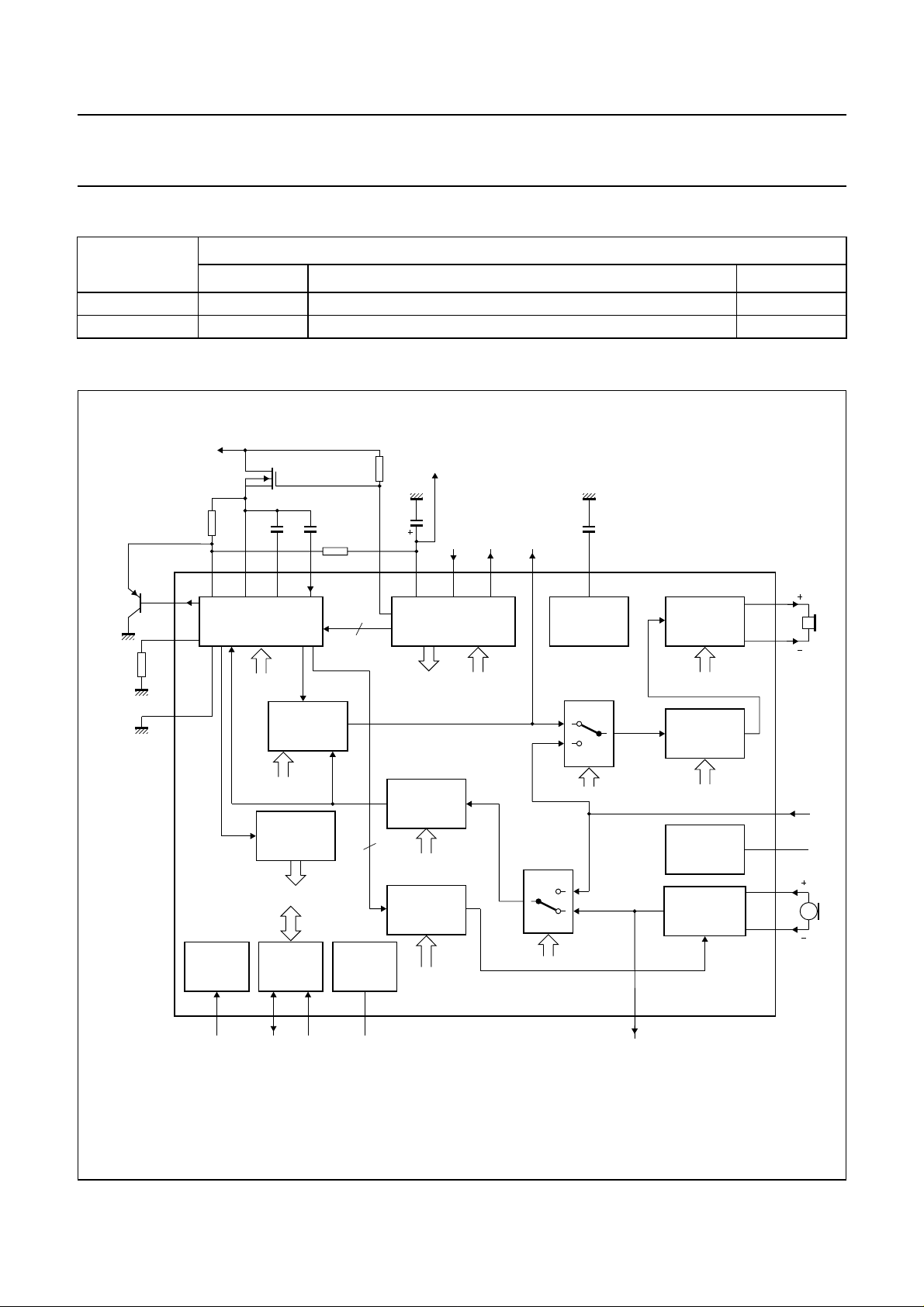
BLOCK DIAGRAM
handbook, full pagewidth
positive line
TX
1
SCR 6
peripheral supply
V
SLPE LN REG LSI DOC
24 5 2 4
LINE INTERFACE POWER CONTROL
DD VMC RMC
PACKAGE
OREC
182223
83
(1)
V
ref
7
BIAS
AND
REFERENCE
BTL RECEIVE
OUTPUT
1415QR
QR
V
SS 13
(1) Test pins.
(2) Default value.
I
line
CLOCK
INTERFACE
19
CLK
V
SLPE
Z
set
DST
sidetone
balance
CONTROL
2
I C-BUS
INTERFACE
ANTI
SIDETONE
GAIN
line current
21
SDA20SCL
TEST
CONTROL
16
TST
PRES PD
PCA1070
SEND
PROG-AMP
(15 dB)
gain G
DYNAMIC
LIMITER
threshold
(1)
ma
maximum level
PROG-AMP
MICROPHONE
MICROPHONE
PREAMPLIFIER
9
(1)
OMIC
load select
RECEIVE
(2)
(-6 dB)
gain G
ra
SUPPLY
(20 dB)
17
10
12
11
MLA944
DTMF
V
P
MIC
MIC
DPI
RRG
(2)
send mute
(0 dB)
(−25 dB)
receive mute
(0 dB)
(0 dB)
Fig.1 Block diagram.
1997 Jun 20 3
Philips Semiconductors Product specification
Multistandard programmable analog
CMOS transmission IC
PINNING
SYMBOL PIN DESCRIPTION
TX 1 drive output
REG 2 voltage regulator decoupling
DOC 3 dial output connection
LSI 4 line signal input
LN 5 positive line terminal
SCR 6 sending current resistor
V
ref
OREC 8 output receiving preamplifier; to be
OMIC 9 output microphone preamplifier;
V
P
MIC− 11 inverting input microphone
MIC+ 12 non-inverting input microphone
V
SS
QR+ 14 non-inverting output of receiving
QR− 15 inverting output of receiving
TST 16 test pin; to be connected to V
DTMF 17 dual tone multi-frequency input
RMC 18 reset output for microcontroller
CLK 19 clock signal input
SCL 20 serial clock line input; I
SDA 21 serial data line input/output; I
VMC 22 input to sense supply voltage
V
DD
SLPE 24 slope (DC resistance) adjustment
7 voltage reference decoupling
left open-circuit in application
to be left open-circuit in application
10 supply for electret microphones
preamplifier
preamplifier
13 negative line terminal
amplifier
amplifier
SS
application
2
C-bus
2
microcontroller
23 positive supply decoupling
C-bus
in
handbook, halfpage
TX
1
REG
2
DOC
3
LSI
4
LN
5
SCR
6
V
ref
OREC
OMIC
V
MIC−
MIC+
PCA1070
7
8
9
10
P
11
12
MGE338
Fig.2 Pin configuration.
PCA1070
SLPE
24
V
23
DD
VMC
22
SDA
21
SCL
20
19
CLK
RMC
18
17
DTMF
TST
16
QR−
15
QR+
14
V
13
SS
1997 Jun 20 4
Philips Semiconductors Product specification
Multistandard programmable analog
CMOS transmission IC
FUNCTIONAL DESCRIPTION
All values in the Chapter “Functional description” are
typical unless stated otherwise.
Line interface
VOLTAGE DROP
DC
Power for the PCA1070 and its peripheral circuits is
obtained from the telephone line. The IC develops its own
supply voltage at VDD and regulates its DC voltage drop
between pins SLPE and VSS. This voltage (V
programmed via the I2C-bus interface between
3.1 to 5.9 V and is default at 4.7 V (see Table 8).
The DC line voltage at pin LN can be calculated using the
following equation:
VLN=V
SLPE
+(I
− ILN) × R
line
LN-SLPE
where:
ILN= DC bias current flowing into pin LN
(≈3 mA if I
R
LN-SLPE
> 17 mA)
line
= external 20 Ω resistor between
LN and SLPE.
At line currents below 6 mA the DC voltage V
automatically adjusted to a lower value. This means that
the operation of more sets, connected in parallel, is
possible with reduced sending and receiving levels and
relaxed performance. At line currents below 16 mA the DC
bias current ILN is reduced from ≈3 mA to a lower value to
ensure maximum possible transmit level capability under
all line current conditions.
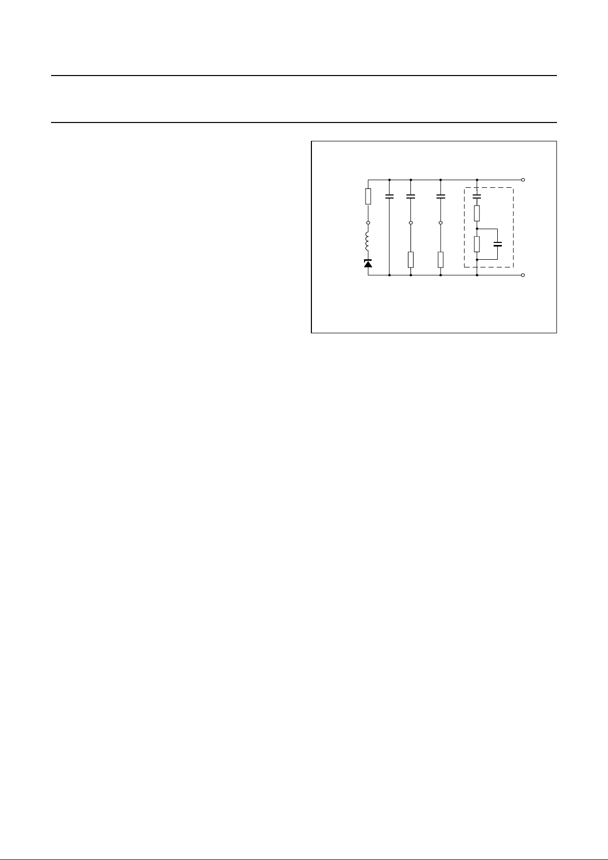
S
ET IMPEDANCE
In normal conditions I
>> ILN and the static behaviour is
line
equivalent to a voltage regulator diode with a series
resistor R
. In the audio frequency range the
LN-SLPE
dynamic impedance ZLN is determined mainly by the
internal component Z
set=Ra
+(Rb// C). The equivalent
impedance ZLN is shown in Fig.3. The values of Ra, R
and C can be programmed via the I2C-bus interface
(see Tables 9, 10 and 11).
SLPE
SLPE
) can be
is
b
PCA1070
handbook, halfpage
R
LN-SLPE
SLPE
L
eq
V
SLPE
where:
Ca= DC blocking capacitor (influence negligible at
f ≥ 300 Hz for given value of C
C
= capacitor at pin LSI (100 nF)
LSI
CP= internal capacitor (12 nF)
C
= capacitor at pin REG (470 nF)
REG
Leq= artificial inductor
(= RP× R
R
LN-SLPE
LN-SLPE
= DC slope resistance (20 Ω)
RP= internal resistor (1075 kΩ at V
R
= internal resistor (240 kΩ).
LSI
S
UPPLY FOR PERIPHERAL CIRCUITS
The supply voltage VDD can be used for peripheral
circuitry. The supply capabilities depend on the
programmed DC voltage drop V
parameters as given in the following equation:
VDD=V
SLPE
where:
IDD= internal current consumption PCA1070 (2.3 mA)
Ip= current to peripheral circuitry
IVP= current taken from VP for electret microphone
R
SLPE−VDD
CPC
REGCLSI
REG LSI
R
R
P
LSI
C
a
Z
set
R
a
C
R
b
MGE342
Fig.3 Equivalent impedance ZLN.
)
LSI
× C
− (IDD+Ip+IVP) × R
= 10.1 H at V
REG
= 4.7 V)
SLPE
= 4.7 V)
SLPE
and on several other
SLPE
SLPE−VDD
= external resistor between SLPE and VDD.
LN
V
SS
1997 Jun 20 5
Philips Semiconductors Product specification
Multistandard programmable analog
CMOS transmission IC
DC STARTING AND SETTLING TIME
The IC is equipped with circuitry for fast DC start-up. This
circuit is automatically activated as soon as VDD reaches
3 V after hook-off, and is deactivated when V
below 5.9 V. This ensures that only a relatively short time
is needed to reach the default DC setting (V
circuit and that VDD will not exceed the maximum permitted
voltage of 6 V.
The start-up circuit can also be activated under software
control by setting bit code DST to logic 1 via the I2C-bus.
The start-up time can be optimized by programming the bit
code DST to logic 1 during the start-up procedure.
In practice this is possible as soon as the microcontroller
has become operational. The DST bit can also be used to
quickly restore the DC settings (V
breaks or during reprogramming of V
) after long line
SLPE
.
SLPE
It should be noted that the AC impedance into pin LN is
reduced considerably when DST = 1.
SLPE
SLPE
drops
) of the
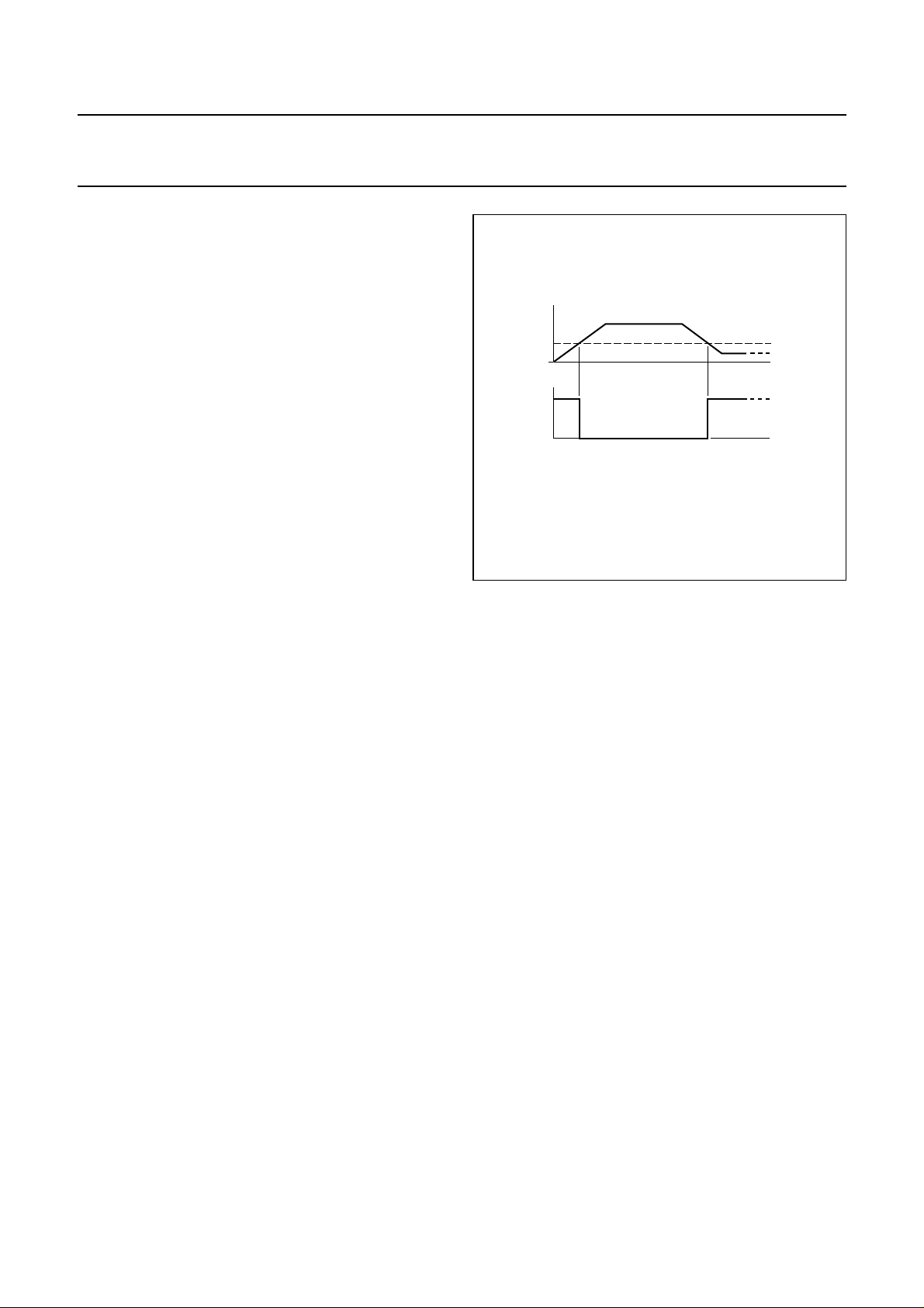
handbook, halfpage
V
VMC
0
RMC
PCA1070
Fig.4 VMC timing diagram.
MGE339
low voltage
condition
V
RESET
logic 1
logic 0
Power control
INTERNAL RESET PCA1070
The PCA1070 has an internal reset circuit that monitors
the supply voltage VDD. If VDD is below the threshold level
(1.2 V) then the circuit is in reset-mode. In this mode the
current consumption is low and the internal reset is active
and writes the default values into all registers. The status
bit PRES will be set to logic 1. The microcontroller can
read this bit via the I2C-bus interface; once read it will be
set to logic 0 again.
When VDD passes the threshold (increasing VDD), the
circuit becomes partly active and the internal ring/speech
detector will be activated (see Section “Start-up and
switch-off behaviour”).
R
ESET OUTPUT FOR MICROCONTROLLER
The voltage at pin VMC (microcontroller supply voltage) is
monitored by a reset circuit. If V
is below the threshold
VMC
level the output RMC is set to logic 1. This threshold level
is 2 V in the normal operating and power-down mode and
2.1 V in the standby mode (see Fig.4).
OWER-DOWN/STANDBY MODES
P
The circuit can be set in power-down or standby mode.
These modes are intended for use with pulse dialling
during long line breaks and applications with memory
retention.
With control bits PDx = 01, the circuit is in the power-down
mode; the typical current consumption at pin VDD is
reduced from IDD= 2.3 mA to 30 µA; the typical current
consumption at pin VMC is 4 µA. When PDx = 11 the
circuit is in the standby mode and I
DD
and I
VMC
are
reduced to 2 µA. In both conditions (power-down and
standby) the voltage stabilizer will be disabled.
S
TART-UP AND SWITCH-OFF BEHAVIOUR
This description refers to the basic application where V
DD
and VMC are connected together and one supply
capacitor is used (see Fig.8).
1997 Jun 20 6

Philips Semiconductors Product specification
Multistandard programmable analog
CMOS transmission IC
Speech condition
After hook-off, line current will be applied to the line input
LN and the supply capacitor connected to VDD and VMC
will be charged.
The internal reset signal will change from logic 1 to logic 0
when VDD passes the threshold level (1.2 V) and the circuit
becomes partly active [the line interface part is kept in
power-down mode, so that all of the line current is
available to charge the supply capacitor(s)];
The PCA1070 can receive data via the I2C-bus (standard
2
C specifications are fulfilled for VDD≥ 2.5 V; relaxed
I
performance for VDD= 1.8 to 2.5 V).
When V
(2.1 V in standby mode) the output RMC changes from
logic 1 to logic 0 and the circuit is switched to the normal
operating mode.
After hook-on V
change from logic 0 to logic 1 when V
threshold level, however the PCA1070 will stay in the
normal operating mode until the internal reset at 1.2 V
takes place.
By decreasing VDD the internal reset signal will change
from logic 0 to logic 1 when VDD passes 1.2 V and the
circuit will go into the reset mode (line interface part in
power-down and all programmable parameters reset to
default values).
Ringer condition
In this condition the supply capacitor connected to VDD and
VMC is charged by the rectified ringer signal; no line
current is applied to pin LN.
passes the microcontroller reset level of 2 V
VMC
decreases and the output RMC will
VMC
passes the
VMC
PCA1070
IAL PULSE INPUT (DPI)
D
The DPI bit controls output DOC (open-drain) that drives
the gate of an external MOS interrupter transistor. DPI is
controlled via the I2C-bus interface.
If DPI is set to logic 1, pin DOC will be pulled down to
switch-off the MOSFET to generate a line break. If DPI = 0
pin DOC is high-ohmic and the interrupter transistor will
conduct the line current.
Sending channel
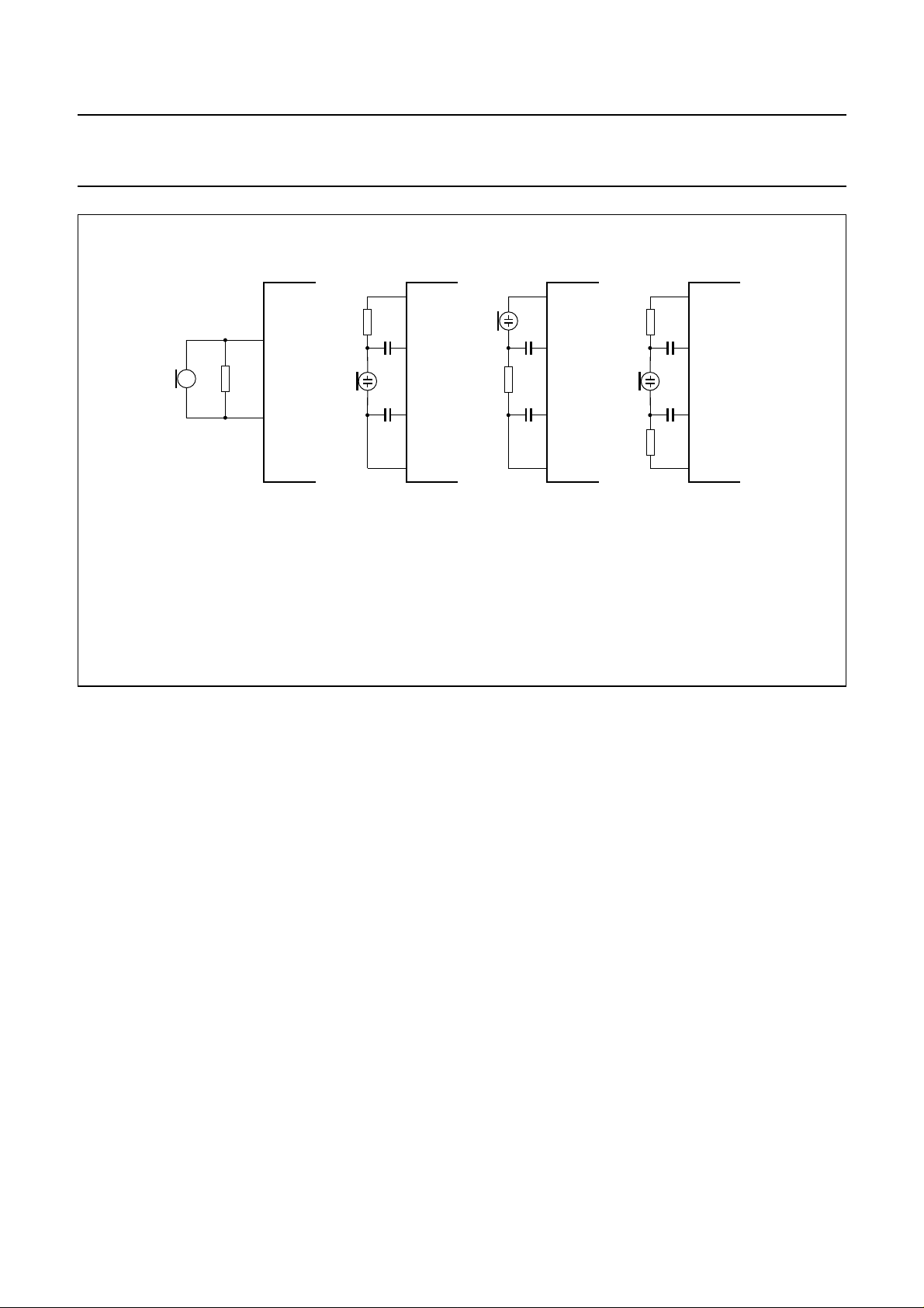
The PCA1070 has symmetrical microphone inputs and
accepts input signals of maximum 70 mV (peak) for
THD = 2% (V
and its gain is default 41 dB. Dynamic, magnetic,
piezoelectric and electret (with built-in FET source
follower) microphones can be used. Some possible
microphone arrangements are shown in Fig.5.
The gain of the sending channel can be programmed
between 30 dB and 51 dB in 1 dB steps using bit code
GMAx (6 bits). The gain of the microphone preamplifier is
20 dB (with dynamic limiter not active) and GMAx sets the
gain of the ‘sending prog-amp’ (allowed range
Gma= 4 to 25 dB). The gain of the line interface is 6 dB.
Thus the total gain of the sending channel (GM) is as
follows:
GM=20+Gma+ 6 (dB)
Default: GM=20+15+6=41dB
Where Gma= ‘gain sending prog-amp’.
Programming the gain of the ‘sending prog-amp’ is given
in Table 13.
≥ 2.5 V). Its input impedance is 100 kΩ
DD
VDD and V
are increasing and when VDD passes the
VMC
internal reset threshold level (1.2 V), the internal
ring/speech-detector will be activated and the circuit will
switch to the standby condition (IDD<5µA; I
VMC
<5µA)
before the voltage at VMC reaches the threshold level for
microcontroller reset. When V
passes this threshold
VMC
level (2.1 V) output RMC changes from logic 1 to logic 0
and the circuit will stay in the standby mode until line
current is applied to pin LN. By setting the ‘Reset Ring’
control bit (RRG) to logic 1 via the I2C-bus interface, the
ring/speech detector will be disabled.
1997 Jun 20 7
Philips Semiconductors Product specification
Multistandard programmable analog
CMOS transmission IC
handbook, full pagewidth
MIC+
MIC−
(a)
(a) Dynamic or piezo.
(b) Low impedance electret with built-in pre-amplifier.
(c) High impedance electret with built-in pre-amplifier.
(d) Symmetrical connection of electret.
(b)
V
P
MIC+
MIC−
V
SS
(c)
V
P
MIC+
MIC−
V
SS
(d)
V
P
MIC+
MIC−
V
SS
MGE341
PCA1070
Fig.5 Microphone arrangements.
Dynamic limiter
To prevent distortion of the transmitted speech signal, the
gain of the microphone amplifier is reduced rapidly when
signal peaks on the line exceed an internally determined
threshold level. The time in which the gain is reduced, the
attack time, is very short. The circuit stays in this
gain-reduced condition until the peaks of the sending
signal remain below the threshold level. The sending gain
then returns to normal after a time also determined on the
chip, the release time. The threshold level of the AC
peak-to-peak line voltage on pin LN is default at
3.5 V (p-p). A level of 2.6 V (p-p) can be programmed by
setting bit code DLT to logic 1.
The internal threshold level is lowered automatically if the
DC voltage setting of the circuit (V
) is not high enough
SLPE
to reach the programmed level. Also when the DC current
in the transmit output stage is insufficient to drive the line
load, the internal threshold level is lowered automatically.
Dynamic limiting considerably improves sidetone
performance in over-drive conditions (less distortion and
limited sidetone level).
DTMF channel
The PCA1070 has an asymmetrical DTMF input. Its input
impedance is 200 kΩ // 45 pF and its gain is default at
21 dB. DTMF signals can be sent to the line by setting
control bit ‘Sending Mute’ (SM) to logic 1 (default SM = 0);
by setting ‘Receiving Mute’ (RM) also to logic 1 (default
RM = 0), the dialling tones are also sent to the receiving
output to generate a confidence tone in the earpiece.
The gain between the DTMF input and the line LN can be
programmed between 1 dB and 21 dB in 1 dB steps using
bit code GMAx (6 bits). The confidence tone gain
(between DTMF input and earpiece outputs QR) can be
programmed between −40 dB and −19 dB (symmetrical
drive of earpiece) using bit code GRAx (6 bits). GMAx sets
the gain of the ‘sending prog-amp’ (recommended range in
DTMF mode for Gma= −5 to 15 dB) and GRAx sets the
gain of the ‘rec prog-amp’ (allowed range
Gra= −25 to 0 dB).
1997 Jun 20 8

Philips Semiconductors Product specification
h
Multistandard programmable analog
CMOS transmission IC
The total gain of the DTMF channel between the DTMF
input and the line LN is as follows:
G
DTMF=Gma
Default G
The confidence tone gain (DTMF to QR outputs) is:
With symmetrical drive of earpiece G
Default G
At low gain settings (Gra< −10 dB), the confidence tone
gain will be slightly higher than the calculated value. This
is caused by a residual signal.
Programming the gain of the ‘sending prog-amp’ and the
‘rec prog-amp’ is given in Table 13.
Receiving channel
The gain of the receiving channel is defined between the
line connection LN and the earpiece outputs QR+ and
QR−. Its voltage gain is default −6 dB (differential drive).
The LN terminal accepts receiving signals up to 1 V (RMS)
for THD = 2%. The outputs may be used to connect
dynamic, magnetic or piezoelectric earpieces with
single-ended or differential drive. The load select bit RFC
is set default to logic 1 to guarantee stable operation in
case of a capacitive load (piezoelectric earpiece). With a
resistive load (dynamic capsule) RFC should be set to
logic 0 via the I
performance with respect to distortion and bandwidth.
Two levels for hearing protection can be selected via the
I2C-bus interface with control bit HPL.
+ 6 (dB)
=15+6=21dB
DTMF
= −6 − 19 = −25 dB.
CTss
2
C-bus interface to obtain optimum
CTs=Gra
− 19 (dB)
PCA1070
The gain of the receiving channel can be programmed
between −19 dB and +11 dB (symmetrical drive) in 1 dB
steps using bit code GRAx (6 bits).
GRAx sets the gain of the ‘rec prog-amp’ (allowed range
Gra= −19 dB to +11 dB; default Gra= −6 dB).
The total gain of the receiving channel is as follows:
Symmetrical drive GRS=Gra(dB)
Default GRS= −6 dB.
Asymmetrical or single-ended drive GRA=GRS− 6 (dB)
Default Gra= −6 − 6 (dB) = −12 dB.
Programming the gain Gra of the ‘rec prog-amp’ is given in
Table 13.
Sidetone balance
The PCA1070 has an on-chip anti-sidetone circuit.
An internal balance impedance Z
via the I
impedance Z
Z
2
oss=Rsa
C-bus interface to match the external line
to give optimum sidetone suppression.
line
+(Rsb// Cs).
Programming the sidetone balance impedance is given in
Tables 14, 15 and 16.
Line current control
The DC line current can be read via the I
This information can be used for the adaptation of
transmission parameters (for example line loss
compensation, sidetone balance and DC characteristic).
can be programmed
oss
2
C-bus interface.
The earpiece arrangements are illustrated in Fig.6.
The bit code LCx as a function of line current is given in
Table 17.
andbook, halfpage
QR+
QR−
(a)
symmetrical
QR+
QR−
V
SS
MGE340
(b)
single-ended
Fig.6 Earpiece arrangements.
1997 Jun 20 9
Philips Semiconductors Product specification
Multistandard programmable analog
CMOS transmission IC
I2C-BUS PROGRAMMING
Table 1 Programmable parameters
The following parameters (see Fig.1) can be programmed by means of a bit code via the I
SYMBOL PARAMETER BLOCK BITS DESCRIPTION
VDCx V
SLPE
line interface 3 DC voltage SLPE-V
ZSAx set impedance line interface 3 Ra of set impedance
ZSBx line interface 3 R
ZSPx line interface 4 f
of set impedance
b
(pole frequency) of set impedance
p
DST DST line interface 1 DC Start Time
PDx PD power control 2 Power-Down
DPI DPI power control 1 Dial Pulse Input
RRG RRG power control 1 Reset RinG detector
HPL maximum receiving level BTL receiving output 1 Hearing Protection Level
RFC load select BTL receiving output 1 Resistive/Capacitive load
ZOSAx sidetone impedance anti-sidetone 4 R
ZOSBx anti-sidetone 4 R
ZOSPx anti-sidetone 4 C
of sidetone impedance
sa
of sidetone impedance
sb
of sidetone impedance
s
RM receiving mute receiving mute 1 Receiving Mute
GRAx gain G
GMAx gain G
ra
ma
receiving prog-amp 6 Gain receiving prog-amp
sending prog-amp 6 Gain sending prog-amp
SM sending mute sending mute 1 Sending Mute
DLT threshold dynamic limiter 1 Dynamic Limiter Threshold
2
C-bus:
SS
PCA1070
Table 2 Readable parameters
2
The following parameters (see also Fig.1) can be read as a bit code via the I
C-bus:
SYMBOL PARAMETER BLOCK BITS DESCRIPTION
PRES PRES power control 1 PCA1070 Reset
LCx line current gain control 5 Line Current
2
I
C interface
The I2C-bus interface (see
“The I2C-bus and how to use it”
12NC: 9398 393 40011) is used to program the transmission
parameters and control functions.
Table 3 Device address
A6 A5 A4 A3 A2 A1 A0 R/
W
0100010X
All functions can be accessed by writing an 8-bit word to the PCA1070. In order to set up the PCA1070, a control
message consisting of the device address, a R/W bit, a subaddress byte and one or more data bytes must be written to
the PCA1070. If more than one data byte follows the subaddress, these bytes are stored in the successive registers by
the automatic increment feature.
1997 Jun 20 10
Philips Semiconductors Product specification
Multistandard programmable analog
PCA1070
CMOS transmission IC
Table 4 The control word format for the slave receiver
DEVICE ADDRESS SUB ADDRESS DATA/CONTROL BYTE
(1)
S01000100
Note
1. This bit is R/
W.
Table 5 Bit arrangement of each data byte used in the control word: PCA1070 receive (see note 1)
FUNCTION
SUB
ADDRESS
DC voltage H00 VDC2 VDC1 VDC0 DST
Sidetone and set
impedance
H01 ZOSB3 ZOSB2 ZOSB1 ZOSB0 ZOSA3 ZOSA2 ZOSA1 ZOSA0
H02 ZOSP3 ZOSP2 ZOSP1 ZOSP0 ZSA2 ZSA1 ZSA0
H03 ZSB2 ZSB1 ZSB0 ZSP3 ZSP2 ZSP1 ZSP0
Sending channel H04 DLT GMA5 GMA4 GMA3 GMA2 GMA1 GMA0
Receiving
H05 RFC HPL GRA5 GRA4 GRA3 GRA2 GRA1 GRA0
channel
Control H06 PD1 PD0 RRG RM SM DPI
A I7 I6 I5 I4 I3 I2 I1 I0 A D7 D6 D5 D4 D3 D2 D1 D0 A P
D7 D6 D5 D4 D3 D2 D1 D0
Note
1. The bits that are not indicated must be set to logic 0.
Table 6 The control word format for the slave transmitter
DEVICE ADDRESS DATA/STATUS BYTE
S01000101
(1)
A D7D6D5D4D3D2D1D0 A P
Note
1. Change in direction of R/
W bit.
Table 7 PCA1070 send
FUNCTION
PCA1070 status PRES
D7 D6 D5 D4 D3 D2 D1 D0
(1)
−−LC4
(2)
LC3
(2)
LC2
(2)
LC1
(2)
LC0
(2)
Notes
1. Indicates if PCA1070 has received internal reset; PRES will be set to logic 1 with internal reset and is set to logic 0
after reading the register via the I2C-bus.
2. Information about value of line current.
1997 Jun 20 11
 Loading...