

Philips pc42va12 DATASHEETS
Philips Semiconductors Programmable Logic Devices Product specification
PLC42VA12
CMOS programmable multi-function PLD
(42 × 105 × 12)
73
October 22, 1993 853–1414 11164
DESCRIPTION
The new PLC42VA12 CMOS PLD from
Philips Semiconductors exhibits a unique
combination of the two architectural concepts
that revolutionized the PLD marketplace.
The Philips Semiconductors unique Output
Macro Cell (OMC) embodies all the
advantages and none of the disadvantages
associated with the “V” type Output Macro
Cell devices. This new design, combined with
added functionality of two programmable
arrays, represents a significant advancement
in the configurability and efficiency of
multi-function PLDs.
The most significant improvement in the
Output Macro Cell structure is the
implementation of the register bypass
function. Any of the 10 J-K/D registers can be
individually bypassed, thus creating a
combinatorial I/O path from the AND array to
the output pin. Unlike other “V” type devices,
the register in the PLC42VA12 Macro Cell
remains fully functional as a buried register.
Both the combinatorial I/O and buried register
have separate input paths (from the AND
array). In most V-type architectures, the
register is lost as a resource when the cell is
configured as a combinatorial I/O. This
feature provides the capability to operate the
buried register independently from the
combinatorial I/O.
The PLC42VA12 is an EPROM-based CMOS
device. Designs can be generated using
Philips Semiconductors SNAP PLD design
software packages or one of several other
commercially available JEDEC standard PLD
design software packages.
FEATURES
•High-speed EPROM-based CMOS
Multi-Function PLD
– Super set of 22V10, 32VX10 and
20RA10 PAL
ICs
•Two fully programmable arrays eliminate
“P-term Depletion”
– Up to 64 P-terms per OR function
•Improved Output Macro Cell Structure
– Individually programmable as:
* Registered Output with feedback
* Registered Input
* Combinatorial I/O with Buried Register
* Dedicated I/O with feedback
* Dedicated Input (combinatorial)
– Bypassed Registers are 100% functional
with separate input and feedback paths
– Individual Output Enable control
functions
* From pin or AND array
•Reprogrammable – 100% tested for
programmability
•Eleven clock sources
•Register Preload and Diagnostic Test Mode
Features
•Security fuse
APPLICATIONS
•Mealy or Moore State Machines
– Synchronous
– Asynchronous
•Multiple, independent State Machines
•10-bit ripple cascade
•Sequence recognition
•Bus Protocol generation
•Industrial control
•A/D Scanning
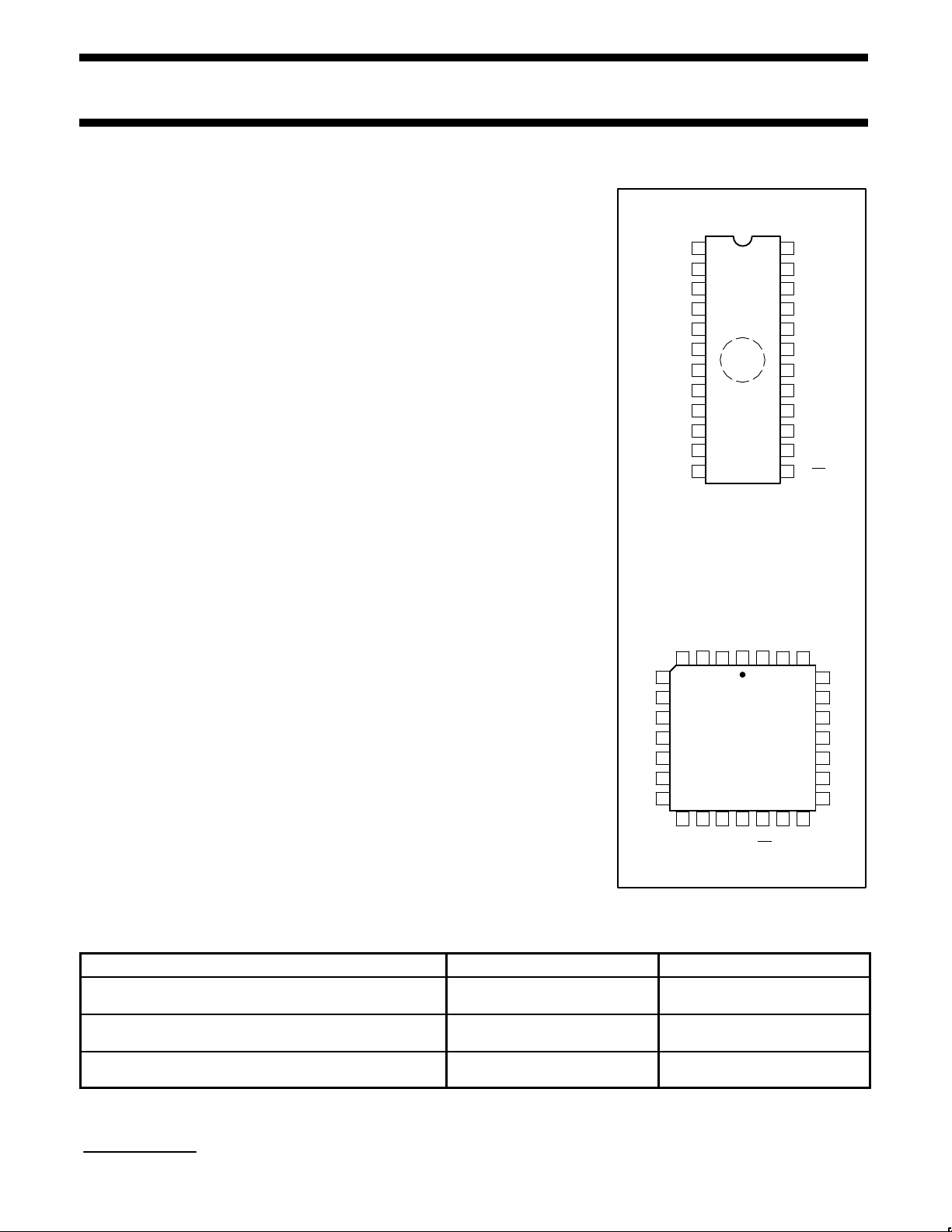
PIN CONFIGURATIONS
I0/
CLK
1
2
3
4
5
6
7
8
9
10
11
12 13
14
15
16
17
18
19
20
21
22
23
24
FA and N Pack-
ages
N = Plastic DIP (300mil-wide)
FA = Ceramic DIP with Quartz Window (300mil-wide)
1234
5
6
7
8
9
10
11
12 13 14 15 16 17 18
19
20
21
22
23
24
25
2627
28
A Package
I0/CLK
I1
I2
I3
I4
I5
I6
I7
I8
B0
B1
GND
I9/OE
M0
M4
M3
M2
M1
M5
M6
M7
M8
M9
V
CC
N/C
N/C
N/C
N/C
I1I2
I3
I4
I5
I6
I7
I8
B0 B1 GND I9/
OE
M0 M1
M2
M3
M4
M5
M6
M7
M8M9
V
CC
A = Plastic Leaded Chip Carrier (450mil-square)
ORDERING INFORMATION
DESCRIPTION ORDER CODE DRAWING NUMBER
24-Pin Ceramic Dual In-Line with window,
Reprogrammable (300mil-wide)
PLC42VA12FA 1478A
24-Pin Plastic Dual In-Line,
One Time Programmable (300mil-wide)
PLC42VA12N 0410D
28-Pin Plastic Leaded Chip Carrier,
One Time Programmable (450mil-wide)
PLC42VA12A 0401F
PAL is a registered trademark of Advanced Micro Devices, Inc.
2
3
4
5
6
7
8
9
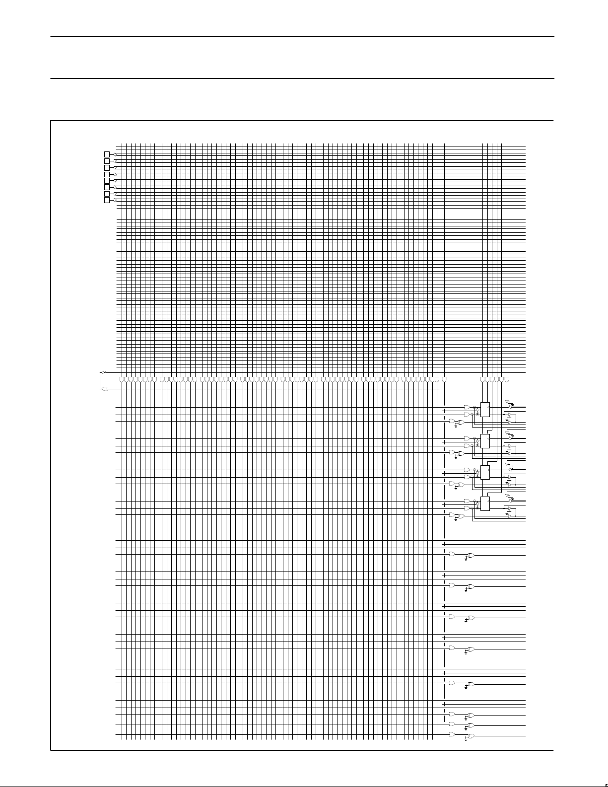
63 56 55 48 47 40 39 32 31 24 23 16 15 8 7 0 F
C
J
K
PR
CK
Q
P
A
R
M
8
R
M
7
R
M
6
R
M
5
C
K
8
I1
I2
I3
I4
I5
I6
I7
I8
J
K
PR
CK
Q
J
K
PR
CK
Q
J
K
PR
CK
Q
NOTE:
Programmable
Connection
Philips Semiconductors Programmable Logic Devices Product specification
PLC42VA12
CMOS programmable multi-function PLD
(42 × 105 × 12)
October 22, 1993
74
LOGIC DIAGRAM
1
21
20
19
18
17
16
15
23
14
11
10
R
M
0
C
K
7
C
K
6
C
K
5
L
A
J
K
PR
CK
Q
J
K
PR
CK
Q
J
K
PR
CK
Q
J
K
PR
CK
Q
J
K
PR
CK
Q
J
K
PR
CK
Q
P
B
R
M
4
R
M
3
R
M
2
R
M
1
C
K
4
C
K
3
C
K
2
C
K
1
L
B
P
M
9
R
M
9
P
M
0
C
K
9
C
K
0
L
M
9
L
M
0
D
M
1
D
M
2
D
M
3
D
M
4
D
M
5
D
M
6
D
M
7
D
M
8
D
M
0
D
M
9
D1D
0
M8
M7
M6
M5
M4
M3
M2
M1
M9
M0
B1
B0
I9/OE
I0/CLK
CK
CK
CK
CK
CK
CK
CK
CK
CK
CK
13
22
Philips Semiconductors Programmable Logic Devices Product specification
PLC42VA12
CMOS programmable multi-function PLD
(42 × 105 × 12)
October 22, 1993
75
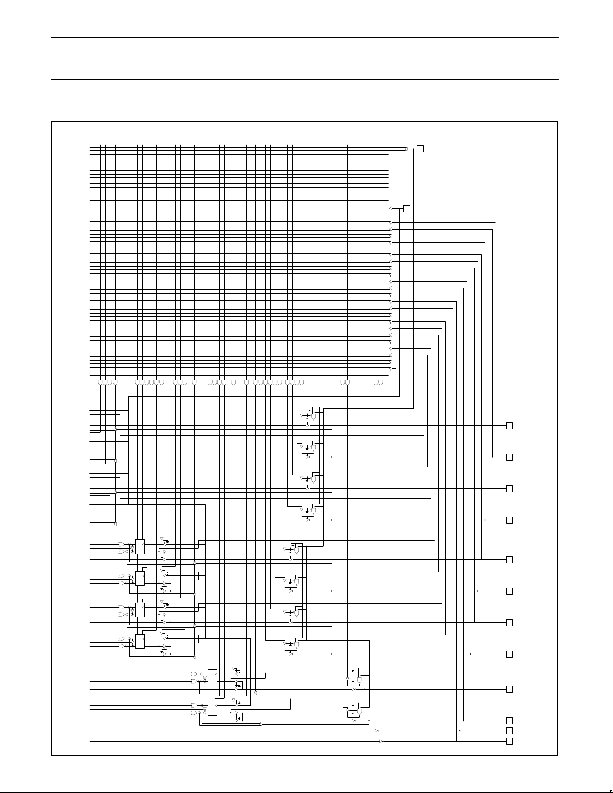
LOGIC DIAGRAM (Continued)

Philips Semiconductors Programmable Logic Devices Product specification
PLC42VA12
CMOS programmable multi-function PLD
(42 × 105 × 12)
October 22, 1993
76
FUNCTIONAL DIAGRAM
P
63
P0F
C
LnPnRnCK
n
LMnPMnRMnCKnDM
n
DM
n
DB
n
I9/OE
I0/CLK
P R
J CK
K Q
X8
P R
J CK
K Q
X2
POLARITY
CLK
CONTROL
OMC
CONFIG.
POLARITY
CLK
CONTROL
OMC
CONFIG.
X8
OE
n
En (X2)
X2
OE
n
En (X2)
X8
X8
X8
X2
POLARITY
X2
X2 X2 X2 X2 X2 X2 X2 X2X8 X8 X8
X8
X2
X2
X1
I1 – I8
M1 – M8
M0, M9
B0 – B1

+5V
C
L
R
1
R
2
S
1
GND
M
Z
M
Z
INPUTS
I
n
I
n
B
M
B
M
OUTPUTS
C
2
C
1
DUT
NOTE:
C
1
and C2 are to bypass VCC to GND.
V
CC
CK
OE
Philips Semiconductors Programmable Logic Devices Product specification
PLC42VA12
CMOS programmable multi-function PLD
(42 × 105 × 12)
October 22, 1993
77
ABSOLUTE MAXIMUM RATINGS
1
THERMAL RATINGS
SYMBOL PARAMETER RATINGS UNIT
V
CC
Supply voltage –0.5 to +7 V
DC
V
IN
Input voltage –0.5 to VCC +0.5 V
DC
V
OUT
Output voltage –0.5 to VCC +0.5 V
DC
I
IN
Input currents –10 to +10 mA
I
OUT
Output currents +24 mA
T
amb
Operating temperature range 0 to +75 °C
T
stg
Storage temperature range –65 to +150 °C
NOTE:
1. Stresses above those listed may cause malfunction or permanent damage to the device. This
is a stress rating only. Functional operation at these or any other condition above those
indicated in the operational and programming specification of the device is not implied.
AC TEST CONDITIONS VOLTAGE WAVEFORMS
MEASUREMENTS:
All circuit delays are measured at the +1.5V level
of inputs and outputs, unless otherwise specified.
Input Pulses
90%
10%
5ns5ns
5ns 5ns
90%
10%
+3.0V
+3.0V
0V
0V
t
RtF
TEMPERATURE
Maximum junction
Maximum ambient
Allowable thermal
rise ambient to
junction
150°C
75
°C
75
°C
Test Load Circuit
Philips Semiconductors Programmable Logic Devices Product specification
PLC42VA12
CMOS programmable multi-function PLD
(42 × 105 × 12)
October 22, 1993
78
DC ELECTRICAL CHARACTERISTICS
0°C ≤ T
amb
≤ +75°C, 4.75V ≤ VCC ≤ 5.25V
LIMITS
SYMBOL PARAMETER TEST CONDITION MIN TYP
1
MAX UNIT
Input voltage
2
V
IL
Low VCC = MIN –0.3 0.8 V
V
IH
High VCC = MAX 2.0 VCC + 0.3 V
Output voltage
2
V
OL
Low VCC = MIN; IOL = 16mA 0.3 0.5 V
V
OH
High VCC = MIN; IOH = –3.2mA 2.4 4.3 V
Input current
I
IL
Low VIN = GND –1 –10 µA
I
IH
High VIN = V
CC
+1 10 µA
Output current
I
O(OFF)
Hi-Z state
V
OUT
= V
CC
V
OUT
= GND
1
–1
10
–10
µA
µA
I
OS
Short-circuit
3,7
V
OUT
= GND –130 mA
I
CC1
VCC supply current (Active)
4
I
OUT
= 0mA, f = 15MHz6, VCC = MAX 90 120 mA
I
CC2
VCC supply current (Active)
5
I
OUT
= 0mA, f = 15MHz6, VCC = MAX 70 100 mA
Capacitance
C
I
Input VCC = 5V; VIN = 2.0V 12 pF
C
B
I/O VB = 2.0V 15 pF
NOTES:
1. All typical values are at V
CC
= 5V. T
amb
= +25°C.
2. All voltage values are with respect to network ground terminal.
3. Duration of short–circuit should not exceed one second. Test one at a time.
4. Tested with V
IL
= 0.45V, VIH = 2.4V.
5. Tested with VIL = 0V, VIH = VCC.
6. Refer to Figure 1, ∆I
CC
vs Frequency (worst case). (Referenced from 15MHz)
The I
CC
increases by 1.5mA per MHz for the frequency range of 16MHz up to 25MHz.
The I
CC
remains at a worst case for the frequency range of 26MHz up to 37MHz.
The I
CC
decreases by 1.0mA per MHz for the frequency range of 14MHz down to 1MHz.
The worst case I
CC
is calculated as follows:
– All dedicated inputs are switching.
– All OMCs are configured as JK flip-flops in the toggle mode. . .all are toggling.
– All 12 outputs are disabled.
– The number of product terms connected does not impact the I
CC
.
7. Refer to Figure 2 for ∆t
PD
vs output capacitance loading.
Figure 1. ∆ICC vs Frequency
(Worst Case) (Referenced from 15MHz)
Figure 2. ∆tPD vs Output
Capacitance Loading (Typical)
f(MHz)
+25
+10
–5
–10
–15
1 5 10 15 20 25 30
I
CC
(mA)
6
5
4
3
2
1
0
–1
–2
0 20 40 60 80 100 120 140 160 180 200
t
PD
OUTPUT CAPACITANCE LOADING (pF)
(ns)
35 40
0
+5
+15
+20
+30
 Loading...