

Philips p8xc557e8 DATASHEETS

INTEGRATED CIRCUITS
DATA SH EET
P8xC557E8
8-bit microcontroller
Product specification
File under Integrated Circuits, IC20
1999 Mar 12

Philips Semiconductors Product specification
8-bit microcontroller P8xC557E8
CONTENTS
1 FEATURES
2 GENERAL DESCRIPTION
2.1 Electromagnetic Compatibility (EMC)
2.2 Recommendation on ALE
3 ORDERING INFORMATION
4 BLOCK DIAGRAM
5 FUNCTIONAL DIAGRAM
6 PINNING INFORMATION
6.1 Pinning diagram
6.2 Pin description
7 FUNCTIONAL DESCRIPTION
8 MEMORY ORGANIZATION
8.1 Program Memory
8.2 Internal Data Memory
8.3 Addressing
9 I/O FACILITIES
10 PULSE WIDTH MODULATED OUTPUTS
(PWM)
10.1 Prescaler Frequency Control Register (PWMP)
10.2 Pulse Width Register 0 (PWM0)
10.3 Pulse Width Register 1 (PWM1)
11 ANALOG-TO-DIGITAL CONVERTER (ADC)
11.1 ADC features
11.2 ADC functional description
11.3 ADC timing
11.4 ADC configuration and operation
11.5 ADC during Idle and Power-down mode
11.6 ADC resolution and characteristics
11.7 ADC after reset
11.8 ADC Special Function Registers
12 TIMERS/COUNTERS
12.1 Timer 0 and Timer 1
12.2 Timer T2
12.3 Watchdog Timer T3
13 SERIAL I/O PORTS
13.1 Serial I/O Port: SIO0 (UART)
13.2 Serial I/O Port: SIO1 (I2C-bus interface)
14 INTERRUPT SYSTEM
14.1 Interrupt Enable Registers
14.2 Interrupt Handling
14.3 Interrupt Priority Structure
14.4 Interrupt vectors
14.5 Interrupt Enable and Priority Registers
15 POWER REDUCTION MODES
15.1 Idle mode
15.2 Power-down mode
15.3 Wake-up from Power-down mode
15.4 Status of external pins
15.5 Power Control Register (PCON)
16 OSCILLATOR CIRCUITS
16.1 XTAL1; XTAL2 oscillator: standard 80C51
16.2 XTAL3; XTAL4 oscillator: 32 kHz PLL oscillator
(with Seconds timer)
17 RESET CIRCUITRY
17.1 Power-on Reset
18 INSTRUCTION SET
18.1 Addressing modes
18.2 80C51 family instruction set
18.3 Instruction set description
19 LIMITING VALUES
20 DC CHARACTERISTICS
21 AC CHARACTERISTICS
22 EPROM CHARACTERISTICS
22.1 Programming and verification
22.2 Security
23 SPECIAL FUNCTION REGISTERS
OVERVIEW
24 PACKAGE OUTLINES
25 SOLDERING
25.1 Introduction
25.2 Reflow soldering
25.3 Wave soldering
25.4 Repairing soldered joints
26 DEFINITIONS
27 LIFE SUPPORT APPLICATIONS
28 PURCHASE OF PHILIPS I2C COMPONENTS
1999 Mar 12 2

Philips Semiconductors Product specification
8-bit microcontroller P8xC557E8
1 FEATURES
• 80C51 Central Processing Unit (CPU)
• 64 kbytes ROM (only P83C557E8)
• 64 kbytes EPROM (only P87C557E8)
• ROM/EPROM Code protection
• 2048 bytes RAM, expandable externally to 64 kbytes
• Two standard 16-bit timers/counters
• An additional 16-bit timer/counter coupled to four
capture registers and three compare registers
• A 10-bit Analog-to-Digital Converter (ADC) with eight
multiplexed analog inputs and programmable autoscan
• Two 8-bit resolution, Pulse Width Modulation outputs
• Five 8-bit I/O ports plus one 8-bit input port shared with
analog inputs
• I2C-bus serial I/O port with byte oriented master and
slave functions
• Full-duplex UART compatible with the standard 80C51
• On-chip Watchdog Timer
• 15 interrupt sources with 2 priority levels (2 to 6 external
sources possible)
• Phase-Locked Loop (PLL) oscillator with 32 kHz
reference and software-selectable system clock
frequency
• Seconds timer
• Software enable/disable of ALE output pulse
• Electromagnetic compatibility improvements
• Wake-up from Power-down by external or seconds
interrupt
• Frequency range for 80C51-family standard oscillator:
3.5 to 16 MHz
• Extended temperature range: −40 to +85 C
• Supply voltage: 4.5 to 5.5 V.
2 GENERAL DESCRIPTION
The 8-bit microcontrollers P80C557E8, P83C557E8 and
P87C557E8 - hereafter referred to as P8xC557E8 - are
manufactured in an advanced CMOS process and are
derivatives of the 80C51 microcontroller family.
The P8xC557E8 contains a volatile 2048 bytes read/write
Data Memory, five 8-bit I/O ports, one 8-bit input port, two
16-bit timer/event counters (identical to the timers of the
80C51), an additional 16-bit timer coupled to capture and
compare latches, a 15-source, two-priority-level,
nested interrupt structure, an 8-input ADC, a dual
Digital-to-Analog Convertor (DAC), Pulse Width
Modulated interface, two serial interfaces (UART and
I2C-bus), a Watchdog Timer, an on-chip oscillator and
timing circuits.
The P8xC557E8 is available in 3 versions:
• P80C557E8: ROMless version
• P83C557E8: containing a non-volatile 64 kbytes mask
programmable ROM
• P87C557E8: containing 64 kbytes programmable
EPROM/OTP.
The P8xC557E8 is a control-oriented CPU with on-chip
Program and Data Memory; it cannot be extended with
external Program Memory. It can access up to 64 kbytes
of external Data Memory. For systems requiring extra
capability, the P8xC557E8 can be expanded using
standard TTL compatible memories and peripherals.
In addition, the P8xC557E8 has two software selectable
reduced power modes: Idle mode and Power-down mode.
The Idle mode freezes the CPU while allowing the RAM,
timers, serial ports, and interrupt system to continue
functioning. The Power-down mode saves the RAM
contents but freezes the oscillator, causing all other chip
functions to be inoperative.The Power-down mode can be
terminated by an external reset, by the seconds interrupt
and by any one of the two external interrupts;
see Section 15.3.
The device also functions as an arithmetic processor
having facilities for both binary and BCD arithmetic as well
as bit-handling capabilities. The instruction set of the
P8xC557E8 is the same as the 80C51 and consists of over
100 instructions: 49 one-byte, 45 two-byte, and
17 three-byte. With a 16 MHz system clock, 58% of the
instructions are executed in 0.75 µs and 40% in 1.5 µs.
Multiply and divide instructions require 3 µs.
1999 Mar 12 3

Philips Semiconductors Product specification
8-bit microcontroller P8xC557E8
2.1 Electromagnetic Compatibility (EMC)
Primary attention is paid to the reduction of
electromagnetic emission of the microcontroller
P8xC557E8. The following features reduce the
electromagnetic emission and additionally improve the
electromagnetic susceptibility:
• Four digital part supply voltage pins (V
four digital ground pins (V
pairs of V
DDn
and V
at two adjacent pins, at each side
SSn
SS1
to V
SS4
DD1
to V
DD4
) and
) are placed as
of the package.
• Separated VDD pins for the internal logic and the port
buffers.
• Internal decoupling capacitance improves the EMC
radiation behaviour and the EMC immunity.
• External capacitors should be connected across
associated V
DDn
and V
pins (i.e. V
SSn
DD1
and V
SS1
).
Lead length should be as short as possible. Ceramic
chip capacitors are recommended (100 nF).
3 ORDERING INFORMATION
PACKAGE
TYPE NUMBER
NAME DESCRIPTION VERSION
P80C557E8EFB
P87C557E8EFB
(1)
(3)
(2)
QFP80
plastic quad flat package;
80 leads (lead length 1.95 mm);
body 14 × 20 × 2.8 mm
2.2 Recommendation on ALE
For applications that require no external memory or
temporarily no external memory: the ALE output signal
(pulses at a frequency of1⁄6× f
) can be disabled under
OSC
software control (bit RFI; SFR: PCON.5); if disabled, no
ALE pulse will occur. ALE pin will be pulled down
internally, switching an external address latch to a quiet
state. The MOVX instruction will still toggle ALE (external
Data Memory is accessed). ALE will retain its normal HIGH
value during Idle mode and a LOW value during
Power-down mode while in the ‘RFI reduction mode’.
Additionally during internal access (EA = 1) ALE will toggle
normally when the address exceeds the internal Program
Memory size. During external access (EA = 0) ALE will
always toggle normally, whether the flag ‘RFI’ is set or not.
FREQUENCY
RANGE (MHZ)
TEMPERATURE
RANGE (°C)
SOT318-2 3.5 to 16 −40 to +85P83C557E8EFB/nnn
Notes
1. ROMless type.
2. ROM coded type; ‘nnn’ denotes the ROM code number.
3. EPROM/OTP type.
1999 Mar 12 4
Philips Semiconductors Product specification
8-bit microcontroller P8xC557E8
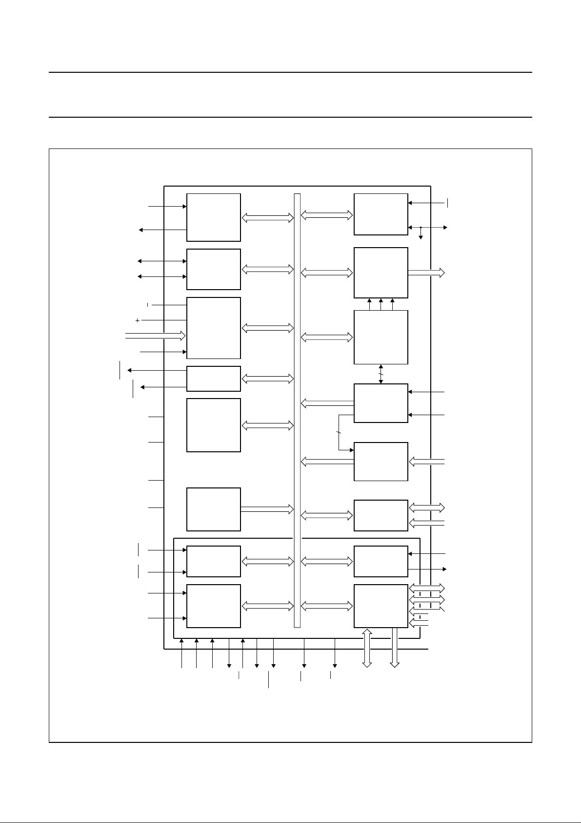
4 BLOCK DIAGRAM
MHI023
XTAL4
XTAL3
+
PLL
'SECONDS'
OSCILLATOR
TIMER
(T3)
TIMER
WATCHDOG
RSTOUT EWCMSR0 to CMSR5
SDA SCL
ref(n)(A)
V
ref(p)(A)
V
ADC0 to ADC7
ADEXS
PWM0
PWM1
SSA
V
DDA
V
SS
V
DD
V
I/O
C-BUS
2
SERIAL
I
(6)
ADC
PWM
DUAL
+
RAM
256 bytes
DATA MEMORY
PROGRAM
1792 bytes
ROM/
MEMORY
64 kbytes
AUX-RAM
(7)
EPROM
P8xC557E8
16
8-bit internal bus
OUTPUT
SELECTION
COMPARATOR
WITH
16-BIT
THREE
COMPARATORS
16
16-BIT
EVENT
TIMER/
FOUR
16-BIT
CAPTURE
I/O
8-BIT
PORTS
REGISTERS
(T2)
COUNTER
LATCHES
(5)(2)(2)(4)(4)
CMT0, CMT1
RT2
T2
handbook, full pagewidth
CT0I to CT3IP4P5RXDTXDP3P2P1P0
Fig.1 Block diagram P8xC557E8.
CPU
core
(T0,T1)
XTAL2
EA
80C51
ALE
excluding
ROM/RAM
PSEN
T1 INT0 INT1
T0
(4) (4) (4) (4)
SELXTAL
EVENT
TIMER/
COUNTERS
TWO 16 - BIT
RSTIN
XTAL1
1999 Mar 12 5
WR
UART
PORT
SERIAL
&
EXT. BUS
PARALLEL
I/O PORTS
(3)
(4)
(4)
RD
(1)
AD0 to AD7
A8 to A15
(1) Alternative function of Port 0.
(2) Alternative function of Port 1.
(3) Alternative function of Port 2.
(4) Alternative function of Port 3.
(5) Alternative function of Port 5.
(6) Alternative function of Port 6.
(7) Not present in P80C557E8.
Philips Semiconductors Product specification
8-bit microcontroller P8xC557E8
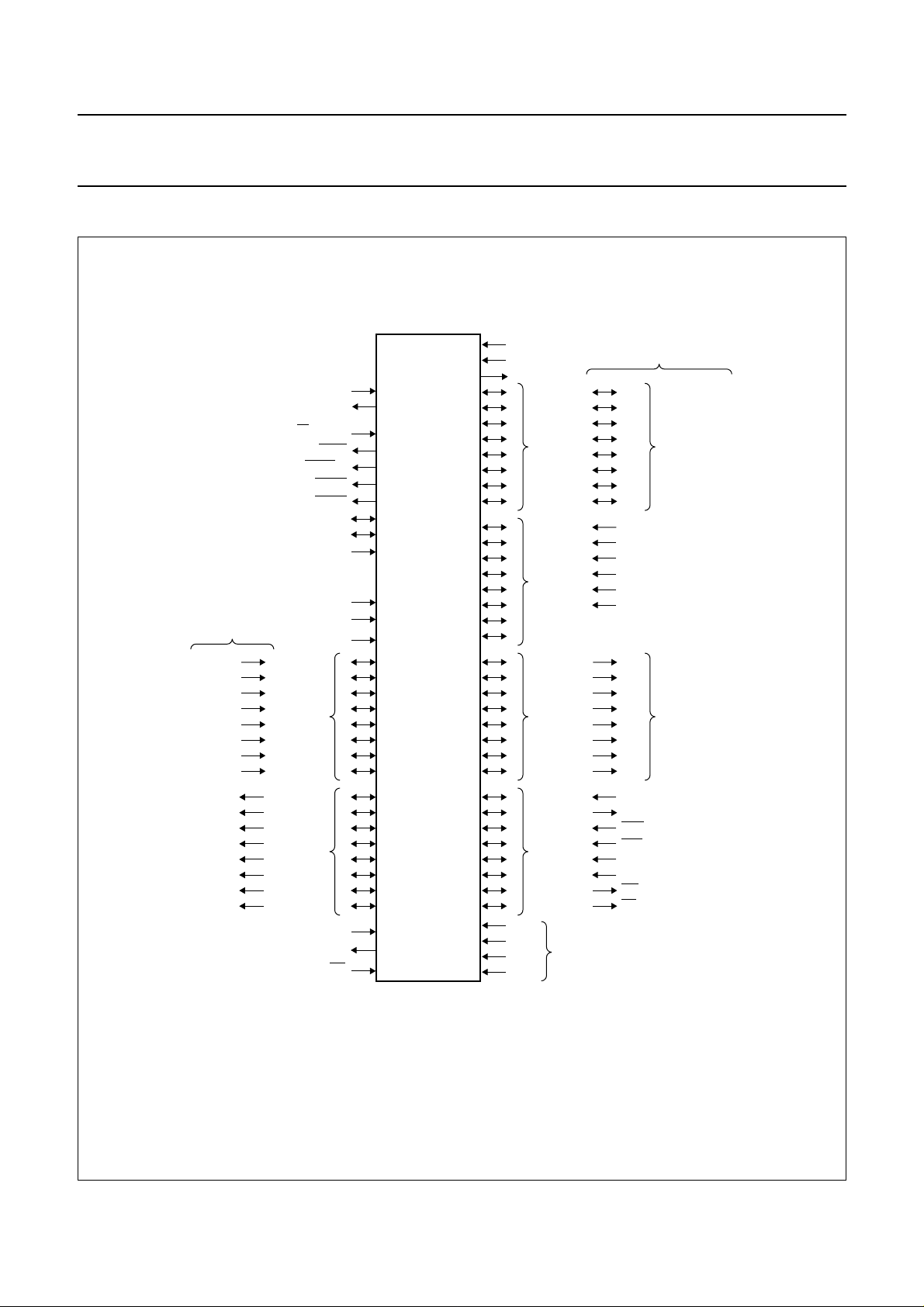
5 FUNCTIONAL DIAGRAM
handbook, full pagewidth
alternative function
ADC0
ADC1
ADC2
ADC3
ADC4
ADC5
ADC6
ADC7
CMSR0
CMSR1
CMSR2
CMSR3
CMSR4
CMSR5
CMT0
CMT1
XTAL1
XTAL2
EA/V
PP
PSEN
ALE/PROG
PWM0
PWM1
SDA
ADEXS
V
ref(p)(A)
V
ref(n)(A)
STADC
PORT 5
PORT 4
RSTIN
RSTOUT
SCL
EW
SELXTAL1
XTAL4
XTAL3
0
1
(1)
(1)
0
1
2
3
4
5
6
7
0
1
2
3
4
5
6
7
P8xC557E8
MHI024
2
3
4
5
6
7
0
1
2
3
4
5
6
7
0
1
2
3
4
5
6
7
0
1
2
3
4
5
6
7
V
V
V
V
SSA
DDA
SS
DD
PORT 0
PORT 1
PORT 2
PORT 3
(2)
alternative function
AD0
AD1
AD2
LOW ORDER
AD3
AD4
AD5
AD6
AD7
CT0I/INT2
CT1I/INT3
CT2I/INT4
CT3I/INT5
A8
A9
A10
A11
A12
A13
A14
A15
RXD/DATA
TXD/CLOCK
INT0
INT1
T0
T1
WR
RD
T2
RT2
ADDRESS
AND
DATA BUS
HIGH ORDER
ADDRESS
BUS
(1) Only the P87C557E8 with an alternative function.
(2) V
VDD/VSS- 4 digital supply pairs.
- 2 analog supply pairs;
DDA/VSSA
Fig.2 Functional diagram.
1999 Mar 12 6
Philips Semiconductors Product specification
8-bit microcontroller P8xC557E8
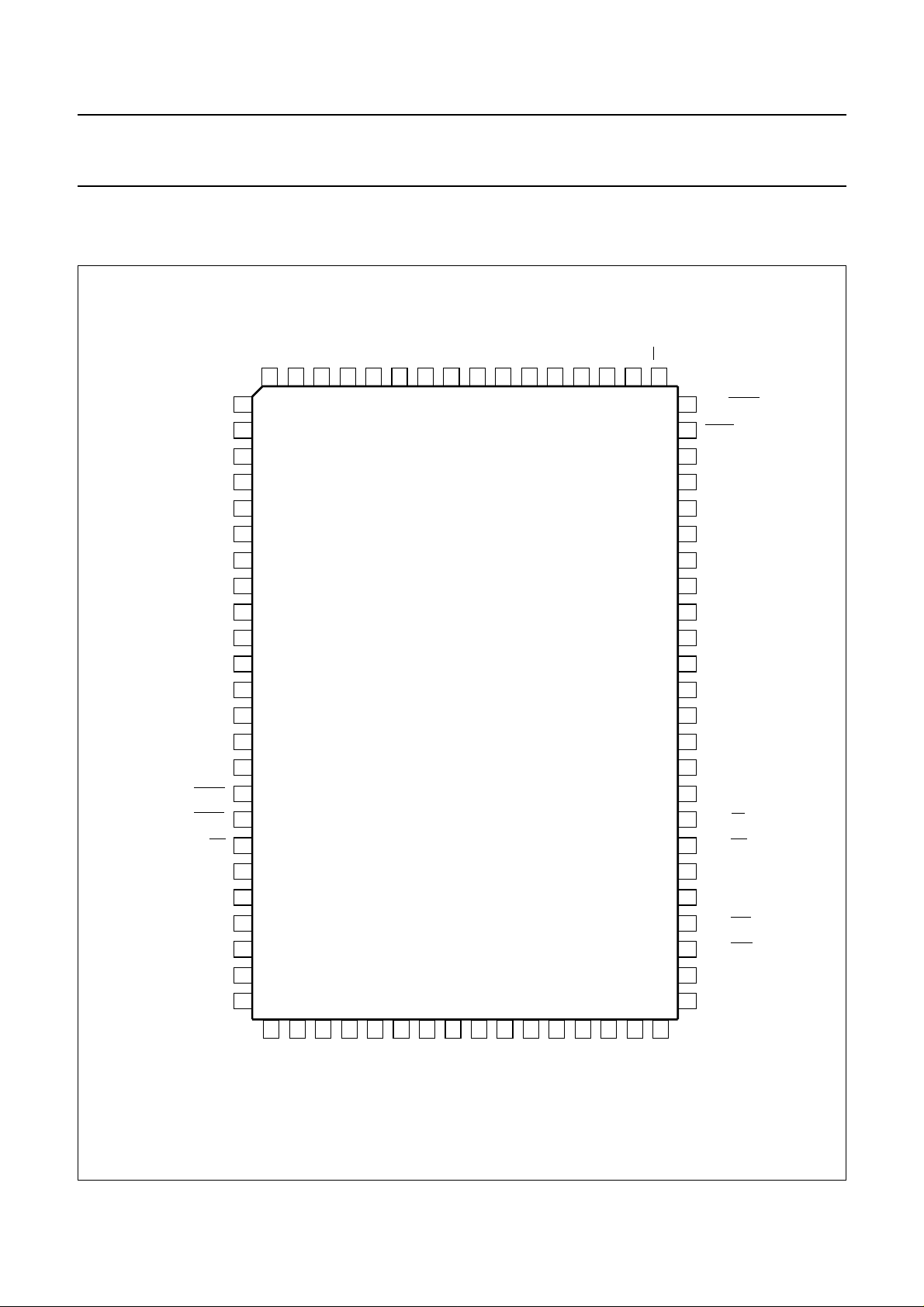
6 PINNING INFORMATION
6.1 Pinning diagram
handbook, full pagewidth
P5.7/ADC7
P5.6/ADC6
P5.5/ADC5
P5.4/ADC4
P5.3/ADC3
P5.2/ADC2
P5.1/ADC1
P5.0/ADC0
V
ref(n)(A)
V
ref(p)(A)
V
SSA1
V
DDA1
V
V
ADEXS
PWM0
SS1
DD1
1
2
3
4
5
6
7
8
9
10
11
12
13
14
15
16
XTAL4
SELXTAL1
80
79
XTAL3
78
SSA2VDDA2
V
76
77
P0.1/AD1
P0.0/AD0
75
74
P8xC557E8
P0.3/AD3
P0.2/AD2
73
72
P0.5/AD5
P0.4/AD4
71
70
P0.7/AD7
P0.6/AD6
69
68
SS4VDD4
V
67
66
(1)
EA/V
65
PP
64
63
62
61
60
59
58
57
56
55
54
53
52
51
50
49
ALE/PROG
PSEN
P2.7/A15
P2.6/A14
P2.5/A13
P2.4/A12
P2.3/A11
P2.2/A10
P2.1/A9
P2.0/A8
V
SS3
V
DD3
XTAL1
XTAL2
n.c.
n.c.
(1)
17
PWM1
18
EW
P4.0/CMSR0
P4.1/CMSR1
P4.2/CMSR2
P4.3/CMSR3
RSTOUT
P4.4/CMSR4
(1) Only the P87C557E8 with this alternative function.
19
20
21
22
23
24
25
26
27
P4.6/CMT0
P4.5/CMSR5
28
DD2
V
P4.7/CMT1
29
V
SS2
30
31
RSTIN
P1.0/CT0I/INT2
Fig.3 Pin configuration QFP80/SOT318 version.
1999 Mar 12 7
32
33
34
P1.1/CT1I/INT3
P1.2/CT2I/INT4
P1.3/CT3I/INT5
35
36
P1.4/T2
P1.5/RT2
37
P1.6
38
P1.7
39
SCL
40
SDA
48
47
46
45
44
43
42
41
P3.7/RD
P3.6/WR
P3.5/T1
P3.4/T0
P3.3/INT1
P3.2/INT0
P3.1/TXD
P3.0/RXD
MHI025
Philips Semiconductors Product specification
8-bit microcontroller P8xC557E8
6.2 Pin description
Table 1 Pin description for QFP80 (SOT318-2)
To avoid a ‘latch-up’ effect at power-on: VSS− 0.5 V < ‘voltage at any pin at any time’ < VDD+ 0.5 V.
SYMBOL PIN DESCRIPTION
V
ref(n)(A)
V
ref(p)(A)
V
SSA1
V
DDA1
P5.7/ADC7 to
P5.0/ADC0
V
to V
V
SS1
DD1
to V
SS4
DD4
ADEXS 15 Start ADC operation. Input starting ADC, triggered by a programmable edge; ADC
PWM0 16 Pulse Width Modulation output 0.
PWM1 17 Pulse Width Modulation output 1.
EW 18 Enable Watchdog Timer (WDT): enable for T3 Watchdog Timer and disable
P4.0/CMSR0 to
P4.5/CMSR5
P4.6/CMT0 to
P4.7/CMT1
RSTOUT 23 Reset output of the P8xC557E8 for resetting peripheral devices during initialization
RSTIN 30 Reset input to reset the P8xC557E8.
P1.0/CT0I/INT2 to
P1.3/CT3I/INT5
P1.4/T2 to
P1.5/RT2
P1.6 to P1.7 37 to 38
SCL 39 I2C-bus serial clock I/O port. If SCL is not used, it must be connected to VSS.
SDA 40 I2C-bus serial data I/O port. If SDA is not used, it must be connected to VSS.
P3.0/RXD 41 Port 3 (P3.0 to P3.7): 8-bit quasi-bidirectional I/O port lines;
P3.1/TXD 42
P3.2/INT0 43
P3.3/INT1 44
P3.4/T0 45
P3.5/T1 46
P3.6/WR 47
P3.7/RD 48
n.c. 49, 50 Not connected pins.
1 Low-end of ADC reference resistor.
2 High-end of ADC reference resistor.
3 Ground, analog part. For ADC receiver and reference voltage.
4 Power supply, analog part (+5 V). For ADC receiver and reference voltage.
5to12 Port 5 (P5.7 to P5.0): 8-bit input port lines;
ADC7 to ADC0: 8 input channels to the ADC.
13, 29,
54, 67
14, 28,
53, 66
Ground; digital part; circuit ground potential. V
V
is internally connected to digital ground, but should be connected externally.
SS3
SS1
, V
SS2
, V
must be connected,
SS4
Power supply, digital part (+5 V). Power supply pins during normal operation and
power reduction modes. All pins must be connected.
operation can also be started by software. This pin must not float.
Power-down mode. This pin must not float.
19 to 22,
24, 25
26, 27
Port 4 (P4.0 to P4.7): 8-bit quasi-bidirectional I/O port lines;
CMSR0 to CMSR5: compare and set/reset outputs for Timer T2;
CMT0 to CMT1: compare and toggle outputs for Timer T2.
and Watchdog Timer overflow.
31 to 34 Port 1 (P1.0 to P1.7): 8-bit quasi-bidirectional I/O port lines;
CT0I to CT3I: Capture timer inputs for Timer T2;
35, 36
INT2 to INT5: external interrupts 2 to 5;
T2: T2 event input (rising edge triggered);
RT2: T2 timer reset input (rising edge triggered).
RXD: Serial input port;
TXD: Serial output port;
INT0: External interrupt input 0;
INT1: External interrupt input 1;
T0: Timer 0 external interrupt input;
T1: Timer 1external interrupt input;
WR: External Data Memory Write strobe;
RD: External Data Memory Read strobe.
1999 Mar 12 8
Philips Semiconductors Product specification
8-bit microcontroller P8xC557E8
SYMBOL PIN DESCRIPTION
XTAL2 51 Crystal pin 2: output of the inverting amplifier that forms the oscillator.
Left open-circuit when an external oscillator clock is used.
XTAL1 52 Crystal pin 1: input to the inverting amplifier that forms the oscillator, and input to the
internal clock generator. Receives the external oscillator clock signal when an external
oscillator is used. Must be connected to logic HIGH if the PLL oscillator is selected
(SELXTAL1 = LOW).
P2.0/A08 to
P2.7/A15
PSEN 63 Program Store Enable output: read strobe to the external Program Memory via
ALE/PROG 64 Address Latch Enable output. Latches the low byte of the address during access of
EA/V
PP
P0.7/AD7 to
P0.0/AD0
V
DDA2
V
SSA2
XTAL3 78 Crystal pin 3: output of the inverting amplifier that forms the 32 kHz oscillator.
XTAL4 79 Crystal pin 2: input to the inverting amplifier that forms the 32 kHz oscillator. XT AL3 is
SELXTAL1 80 SELXTAL1 = HIGH, selects the HF oscillator, using the XTAL1/XTAL2 crystal.
55 to 62 Port 2 (P2.0 to P2.7): 8-bit quasi-bidirectional I/O port lines;
A08 to A15: High-order address byte for external memory.
Ports 0 and 2. Is activated twice each machine cycle during fetches from external
Program Memory . When executing out of externalProgram Memory two activations of
PSEN are skipped during each access to external Data Memory. PSEN is not
activated (remains HIGH) during no fetches from external Program Memory. PSEN
can sink/source 8 LSTTL inputs. It can drive CMOS inputs without external pull-ups.
external memory in normal operation. It is activated every six oscillator periods except
during an external Data Memory access. ALE can sink/source 8 LSTTL inputs. It can
drive CMOS inputs without an external pull-up. To prohibit the toggling of ALE pin (RFI
noise reduction) the bit RFI (SFR: PCON.5) must be set by software; see Section 2.2.
PROG: the programming pulse input; alternative function for the P87C557E8.
65 External Access input. If, during reset, EA is held at a TTL level HIGH the CPU
executes out of the internal Program Memory. If, during reset, EA is held at a TTL level
LOW the CPU executes out of external Program Memory via Port 0 and Port 2. EA is
not allowed to float. EA is latched during reset and don’t care after reset.
VPP: the programming supply voltage; alternative function for the P87C557E8.
68 to 75 Port 0 (P0.7 to P0.0): 8-bit open-drain bidirectional I/O port lines;
AD7 to AD0: Multiplexed Low-order address and Data bus for external memory.
76 Power supply, analog part (+5 V). For PLL oscillator.
77 Ground, analog part. For PLL oscillator.
pulled LOW if the PLL oscillator is not selected (SELXTAL1 = 1) or if reset is active.
If SELXTAL1 = LOW the PLL is selected for clocking of the controller, using the
XTAL3/XTAL4 crystal.
1999 Mar 12 9

Philips Semiconductors Product specification
8-bit microcontroller P8xC557E8
7 FUNCTIONAL DESCRIPTION
The P8xC557E8 is a stand-alone high-performance
microcontroller designed for use in real time applications
such as instrumentation, industrial control, medium to
high-end consumer applications and specific automotive
control applications.
In addition to the 80C51 standard functions, the device
provides a number of dedicated hardware functions for
these applications.
The P8xC557E8 is a control-oriented CPU with on-chip
program and Data Memory, but it cannot be extended with
external Program Memory. It can access up to 64 kbytes
of external Data Memory. For systems requiring extra
capability, the P8xC557E8 can be expanded using
standard memories and peripherals.
The functional description of the device is described in:
Chapter 8 “Memory organization”
Chapter 9 “I/O facilities”
Chapter 10 “Pulse Width Modulated outputs”
Chapter 11 “Analog-to-Digital Converter (ADC)”
Chapter 12 “Timers/counters”
Chapter 13 “Serial I/O ports”
Chapter 14 “Interrupt system”
Chapter 15 “Reduced power modes”
Chapter 16 “Oscillator circuits”
Chapter 17 “Reset circuitry”.
1999 Mar 12 10

Philips Semiconductors Product specification
8-bit microcontroller P8xC557E8
8 MEMORY ORGANIZATION
The Central Processing Unit (CPU) manipulates operands
in three memory spaces; these are the 64 kbytes external
Data Memory, 2048 bytes internal Data Memory
(consisting of 256 bytes standard RAM and 1792 bytes
AUX-RAM) and the 64 kbytes internal or 64 kbytes
external Program Memory (see Fig.4).
8.1 Program Memory
The Program Memory of the P8xC557E8 consists of
64 kbytes ROM or 64 kbytes EPROM. If, during reset, the
EA pin was held HIGH, the P8xC557E8 always executes
out of the internal Program Memory. If the EA pin was held
LOW during reset the P8xC557E8 fetches all instructions
from the external Program Memory. The EA input is
latched during reset and is don’t care after reset.
The internal Program Memory content is protected by
setting a mask programmable security bit (ROM) or by the
software programmable security bits (EPROM)
respectively, i.e. it cannot be read out at any time by any
test mode or by any instruction in the external Program
Memory space. The MOVC instructions are the only ones
which have access to program code in the internal or
external Program Memory. The EA input is latched during
reset and is don’t care after reset. This implementation
prevents from reading internal program code by switching
from external Program Memory to internal Program
Memory during MOVC instruction or an instruction that
handles immediate data. Table 2 lists the access to the
internal and external Program Memory with MOVC
instructions whether the security feature has been
activated or not.
Due to the maximum size of the internal Program Memory,
the MOVC instructions can always operate either in the
internal or in the external Program Memory.
Table 2 Memory access by the MOVC instruction
For code protection of the P87C557E8 see Section 23.2.
8.2 Internal Data Memory
The internal Data Memory is divided into three physically
separated parts: 256 bytes of RAM, 1792 bytes of
AUX-RAM, and a 128 bytes Special Function Registers
(SFRs) area. These parts can be addressed each in a
different way as described in Sections 8.2.1 to 8.2.2 and
Table 3.
Table 3 Internal Data Memory map
MEMORY LOCATION ADDRESS MODE
RAM 0 to 127 Direct and indirect
128 to 255 Indirect only
SFR 128 to 255 Direct only
AUX-RAM 0 to 1791 Indirect only with MOVX
8.2.1 RAM
• RAM 0 to 127 can be addressed directly and indirectly
as in the 80C51. Address pointers are R0 and R1 of the
selected register bank.
• RAM 128 to 255 can only be addressed indirectly.
Address pointers are R0 and R1 of the selected register
bank.
Four register banks, each 8 registers wide, occupy
locations 0 through 31 in the lower RAM area. Only one of
these banks may be enabled at a time. The next 16 bytes,
locations 32 through 47, contain 128 directly addressable
bit locations. The stack can be located anywhere in the
internal 256 bytes RAM. The stack depth is only limited by
the available internal RAM space of 256 bytes (see Fig.6).
All registers except the Program Counter and the four
register banks reside in the Special Function Register
address space.
8.2.2 SPECIAL FUNCTION REGISTERS
The Special Function Registers can only be addressed
directly in the address range from 128 to 255 (see Fig.7).
MOVC
INSTRUCTION
MOVC in internal
Program Memory
MOVC in external
Program Memory
Note
1. Not applicable due to 64 kbytes internal Program
Memory.
1999 Mar 12 11
PROGRAM MEMORY ACCESS
INTERNAL EXTERNAL
YES NO
(1)
NO
(1)
YES
8.2.3 AUX-RAM
• AUX-RAM 0 to 1791 is indirectly addressable via page
register (XRAMP) and MOVX-Ri instructions, unless it is
disabled by setting ARD = 1 (see Fig.5). When
executing from internal Program Memory, an access to
AUX-RAM 0 to 1791 will not affect the ports P0, P2,
P3.6 and P3.7.
• AUX-RAM 0 to 1791 is also indirectly addressable as
external Data Memory locations 0 to 1791 via MOVX-Ri
instructions, unless it is disabled by setting ARD = 1.
Philips Semiconductors Product specification
8-bit microcontroller P8xC557E8
An access to external Data Memory locations higher than
1791 will be performed with the MOVX @DPTR
instructions in the same way as in the 80C51 structure, so
with P0 and P2 as data/address bus and P3.6 and P3.7 as
write and read timing signals.
Note that the external Data Memory cannot be accessed
with R0 and R1 as address pointer if the AUX-RAM is
enabled (ARD = 0, default).
Table 4 AUX-RAM Page Register (address FAH)
76543210
XRAMPx XRAMPx XRAMPx XRAMPx XRAMPx XRAMP2 XRAMP1 XRAMP0
Table 5 Description of XRAMP bits
BIT SYMBOL FUNCTION
7 to 3 XRAMPx Reserved for future use. During read XRAMPx = undefined; a write
operation must write logic 0s to these locations.
2 to 0 XRAMP2 to XRAMP0 AUX-RAM page select bits 2 to 0; see Table 6.
Table 6 Memory locations for all possible MOVX-accesses
X = don’t care.
(1)
ARD
XRAMP2 XRAMP1 XRAMP0 MEMORY LOCATIONS
8.2.4 AUX-RAM PAGE REGISTER (XRAMP)
The AUX-RAM Page Register is used to select one of
seven 256-bytes pages of the internal 1792 bytes
AUX-RAM for MOVX-accesses via R0 or R1. Its reset
value is ‘XXXXX000B’.
MOVX @Ri,A and MOVX A,@Ri instructions access
0 0 0 0 AUX-RAM locations 0 to 255 (reset condition)
0 0 0 1 AUX-RAM locations 256 to 511
0 0 1 0 AUX-RAM locations 512 to 767
0 0 1 1 AUX-RAM locations 768 to 1023
0 1 0 0 AUX-RAM locations 1024 to 1279
0 1 0 1 AUX-RAM locations 1280 to 1535
0 1 1 0 AUX-RAM locations 1536 to 1791
0 1 1 1 No valid memory access; reserved for future use
1 X X X External RAM locations 0 to 255
MOVX @DPTR,A and MOVX A,@DPTR instructions access
0 X X X AUX-RAM locations 0 to 1791 (reset condition);
External RAM locations 1792 to 65535
1 X X X External RAM locations 0 to 65535
Note
1. ARD: AUX-RAM disable, is a bit in SFR PCON (bit PCON.6); see Section 15.5.
1999 Mar 12 12

Philips Semiconductors Product specification
8-bit microcontroller P8xC557E8
andbook, full pagewidth
64 kbytes
64 kbytes 64 kbytes
INTERNAL
(EA = 1)
0
PROGRAM MEMORY
handbook, full pagewidth
EXTERNAL
(EA = 0)
MOVX @Ri, A
MOVX A, @Ri
OVERLAPPED SPACE
255
INDIRECT ONLY
127
DIRECT AND
INDIRECT
00
MAIN RAM
SPECIAL
FUNCTION
REGISTERS
INTERNAL DATA
MEMORY
AUXILIARY
RAM
(ARD = 0)
1792 bytes
1791
EXTERNAL DATA
(ARD = 1)
MEMORY
MBH077
Fig.4 Memory map and address space.
255 1791
(XRAMP) = 06 H
0
255
(XRAMP) = 05 H
0
255
(XRAMP) = 04 H
0
255
(XRAMP) = 03 H
0
255
(XRAMP) = 02 H
0
255
(XRAMP) = 01 H
0
255
(XRAMP) = 00 H
0
1536
1535
1280
1279
1024
1023
768
767
512
511
256
255
0
MOVX @DPTR, A
MOVX A, @DPTR
MBH078
Fig.5 Indirect addressing AUX-RAM (1792 bytes); ARD = 0 (bit PCON.6).
1999 Mar 12 13
Philips Semiconductors Product specification
8-bit microcontroller P8xC557E8
8.3 Addressing
The P8xC557E8 has five methods for addressing:
• Register
• Direct
• Register-Indirect
• Immediate
• Base-Register plus Index-Register-Indirect.
The first three methods can be used for addressing
destination operands. Most instructions have a
‘destination/source’ field that specifies the data type,
addressing methods and operands involved.
For operations other than MOVs, the destination operand
is also a source operand.
Access to memory addresses is as follows:
• Register in one of the four register banks through
Register, Direct or Register-Indirect addressing.
• Internal RAM (2048 bytes) through Direct or
Register-Indirect addressing.
– Internal RAM: bytes 0 to 127; may be addressed
directly/indirectly.
– Internal RAM: bytes 128 to 255; share their address
location with the SFRs and so may only be addressed
indirectly as data RAM.
– AUX-RAM: bytes 0 to 1791; can only be addressed
indirectly via MOVX.
• Special Function Registers through direct addressing at
address locations 128 to 255 (see Fig.7).
• External Data Memory through Register-Indirect
addressing.
• Program Memory look-up tables through Base-Register
plus Index-Register-Indirect addressing.
BYTE
ADDRESS
(HEX)
FFH
2FH
2EH
2DH
2CH
2BH
2AH
29H
28H
27H
26H
25H
24H
23H
22H
21H
20H
1FH
18H
17H
10H
0FH
08H
07H
00H
BIT ADDRESS
(HEX)
(MSB) (LSB)
7F 7E 7D 7C 7B 7A 79 78
77 76 75 74 73 72 71 70
6F 6E 6D 6C 6B 6A 69 68
67 66 65 64 63 62 61 60
5F 5E 5D 5C 5B 5A 59 58
57 56 55 54 53 52 51 50
4F 4E 4D 4C 4B 4A 49 48
47 46 45 44 43 42 41 40
3F 3E 3D 3C 3B 3A 39 38
37 36 35 34 33 32 31 30
2F 2E 2D 2C 2B 2A 29 28
27 26 25 24 23 22 21 20
1F 1E 1D 1C 1B 1A 19 18
17 16 15 14 13 12 11 10
0F 0E 0D 0C 0B 0A 09 08
07 06 05 04 03 02 01 00
BANK 3
BANK 2
BANK 1
BANK 0
MBH079
BYTE
ADDRESS
(DECIMAL)
255
47
46
45
44
43
42
41
40
39
38
37
36
35
34
33
32
31
24
23
16
15
8
7
0
1999 Mar 12 14
Fig.6 Internal MAIN RAM bit addresses.
Philips Semiconductors Product specification
8-bit microcontroller P8xC557E8
handbook, full pagewidth
BYTE ADDRESS
(HEX)
FFH
F8H
F0H F6 F5 F4 F3 F2 F1 F0
F8H EE ED EC EB EA E9 E8
E0H E6 E5 E4 E3 E2 E1 E0
D8H
D0H
C8H
C0H C6 C5 C4 C3 C2 C1 C0
B8H BE BD BC BB BA B9 B8
B0H B6 B5 B4 B3 B2 B1 B0
A8H AE AD AC AB AA A9 A8
BIT ADDRESS
(HEX)
(MSB) (LSB)
PT2 PCM2 PCM1 PCM0 PCT3 PCT2 PCT1 PCT0
FF
FE FD FC FB FA F9 F8
F7
ET2 ECM2 ECM1 ECM0 ECT3 ECT2 ECT1 ECT0
EF
E7
CR2 ENS1 STA STO SI AA CR1 CR0
DF
DE DD DC DB DA D9 D8
CY AC F0 RS1 RS0 OV F1 P
D7 D6 D5 D4 D3 D2 D1 D0
T2OV CMI2 CMI1 CMI0 CTI3 CTI2 CTI1 CTI0
CF CE CD CC CB CA C9 C8
C7
- PAD PS1 PS0 PT1 PX1 PT0 PX0
BF
B7
EA EAD ES1 ES0 ET1 EX1 ET0 EX0
AF
REGISTER
(MNEMONIC)
IP1
B
IEN1
ACC
S1CON
PSW
TM2IR
P4
IP0
P3
IEN0
A0H A6 A5 A4 A3 A2 A1 A0
A7
SM0 SM1 SM2 REN TB8 RB8 TI RI
98H 9E 9D 9C 9B 9A 99 98
90H 96 95 94 93 92 91 90
88H 8E 8D 8C 8B 8A 89 88
80H 86 85 84 83 82 81 80
9F
97
TF1 TR1 TF0 TR0 IE1 IT1 IE0 IT0
8F
87
MBH456
Fig.7 Special Function Registers bit addresses.
P2
S0CON
P1
TCON
P0
1999 Mar 12 15
Philips Semiconductors Product specification
8-bit microcontroller P8xC557E8
9 I/O FACILITIES
The P8xC557E8 has six 8-bit ports. Ports 0 to 3 are the
same as in the 80C51, with the exception of the additional
functions of Port 1. The parallel I/O function of Port 4 is
equal to that of Ports 1, 2 and 3. All ports are bidirectional
with the exception of Port 5 which is only a parallel input
port.
Ports 0, 1, 2, 3, 4 and 5 perform the following alternative
functions:
Port 0 Provides the multiplexed low-order address and
data bus used for expanding the P8xC557E8 with
standard memories and peripherals.
Port 1 Is used for a number of special functions:
• 4 capture inputs (or external interrupt request
inputs if capture information is not utilized)
• external counter input
• external counter reset input.
Port 2 Provides the high-order address bus when the
P8xC557E8 is expanded with external Data
Memory and / or the P8xC557E8 executes from
external Program Memory.
Port 3 Pins can be configured individually to provide:
• External interrupt request inputs
• Counter inputs
• Receiver input and transmitter output of serial
port SIO 0 (UART)
• Control signals to read and write external Data
Memory.
Port 4 Can be configured to provide signals indicating a
match between timer/counter T2 and its compare
registers.
Port 5 May be used in conjunction with the ADC interface.
Unused analog inputs can be used as digital inputs.
As Port 5 lines may be used as inputs to the ADC,
these digital inputs have an inherent hysteresis to
prevent the input logic from drawing too much
current from the power lines when driven by analog
signals. Channel-to-channel crosstalk should be
taken into consideration when both digital and
analog signals are simultaneously input to Port 5
(see Chapter 21).
A pin of which the alternative function is not used may be
used as normal bidirectional I/O. The generation or use of
a Port 1, Port 3 or Port 4 pin as an alternative function is
carried out automatically by the P8xC557E8 provided the
associated Special Function Register bit is set HIGH.
The SDA and SCL lines serve the serial port SI01
(I2C-bus). Because the I2C-bus may be active while the
device is disconnected from VDD, these pins are provided
with open-drain drivers.
Figure 8 shows the pull-up arrangements of Ports 1 to 4;
Transistor ‘p1’ is turned on for 2 oscillator periods after Q
makes a HIGH-to-LOW transition. During this time, ‘p1’
also turns on ‘p3’ through the inverter to form an additional
pull-up.
handbook, full pagewidth
from port latch
read port pin
input data
2 oscillator
periods
Q
strong pull-up
INPUT
BUFFER
Fig.8 I/O buffers in the P8xC557E8 (Port 1 to Port 4).
1999 Mar 12 16
V
DD
p2
p1
n
p3
I/O PIN
I1
MLC926 - 1

Philips Semiconductors Product specification
8-bit microcontroller P8xC557E8
10 PULSE WIDTH MODULATED OUTPUTS
The P8xC557E8 contains two Pulse Width Modulated
(PWM) output channels (see Fig.9). These channels
generate pulses of programmable length and interval.
The repetition frequency is defined by an 8-bit prescaler
PWMP, which supplies the clock for the counter.
The prescaler and counter are common to both PWM
channels. The 8-bit counter counts modulo 255, i.e., from
0 to 254 inclusive. The value of the 8-bit counter is
compared to the contents of two registers: PWM0 and
PWM1.
Provided the contents of either of these registers is greater
than the counter value, the corresponding PWM0 or
PWM1 output is set LOW. If the contents of these registers
are equal to, or less than the counter value, the output will
be HIGH. The pulse-width-ratio is therefore defined by the
contents of the registers PWM0 and PWM1.
255
255
255
to
⁄
and
255
.
The pulse-width-ratio is in the range of0⁄
may be programmed in increments of1⁄
Buffered PWM outputs may be used to drive DC motors.
The rotation speed of the motor would be proportional to
the contents of PWMn. The PWM outputs may also be
configured as a dual DAC.
In this application, the PWM outputs must be integrated
using conventional operational amplifier circuitry. If the
resulting output voltages have to be accurate, external
buffers with their own analog supply should be used to
buffer the PWM outputs before they are integrated.
The repetition frequency f
=
given by:
f
PWM
--------------------------------------------------------------2 PWMP 1+()× 255×
, at the PWMn outputs is
PWM
f
CLK
This gives a repetition frequency range of 123 Hz to
31.4 kHz (at f
= 16 MHz). By loading the PWM registers
clk
with either 00H or FFH, the PWM channels will output a
constant HIGH or LOW level, respectively. Since the 8-bit
counter counts modulo 255, it can never actually reach the
value of the PWM registers when they are loaded with
FFH.
When a compare register (PWM0 or PWM1) is loaded with
a new value, the associated output is updated
immediately. It does not have to wait until the end of the
current counter period. Both PWMn output pins are driven
by push-pull drivers. These pins are not used for any other
purpose.
handbook, full pagewidth
PWM0
I
N
T
f
E
R
N
A
L
B
U
S
clk
PRESCALER
PWMP
8-BIT COMPARATOR
8-BIT COUNTER1/2
8-BIT COMPARATOR
PWM1
Fig.9 Functional diagram of Pulse Width Modulated outputs.
OUTPUT
BUFFER
OUTPUT
BUFFER
PWM0
PWM1
MGA154
1999 Mar 12 17

Philips Semiconductors Product specification
8-bit microcontroller P8xC557E8
10.1 Prescaler Frequency Control Register (PWMP)
Reading PWMP gives the current reload value. The actual count of the prescaler cannot be read.
Table 7 Prescaler Frequency Control Register (address FEH)
76543210
PWMP.7 PWMP.6 PWMP.5 PWMP.4 PWMP.3 PWMP.2 PWMP.1 PWMP.0
Table 8 Description of PWMP bits
BIT SYMBOL DESCRIPTION
7 to 0 PWMP.7 to PWMP.0 Prescaler division factor. The Prescaler division factor = (PWMP) + 1.
10.2 Pulse Width Register 0 (PWM0)
Table 9 Pulse width register (address FCH)
76543210
PWM0.7 PWM0.6 PWM0.5 PWM0.4 PWM0.3 PWM0.2 PWM0.1 PWM0.0
Table 10 Description of PWM0 bits
BIT SYMBOL DESCRIPTION
7 to 0 PWM0.7 to PWM0.0
10.3 Pulse Width Register 1 (PWM1)
Table 11 Pulse width register (address FDH)
76543210
PWM1.7 PWM1.6 PWM1.5 PWM1.4 PWM1.3 PWM1.2 PWM1.1 PWM1.0
Table 12 Description of PWM1 bits
BIT SYMBOL DESCRIPTION
7 to 0 PWM1.7 to PWM1.0
Pulse width ratio.
LOW/HIGH ratio of PWM0 signals
Pulse width ratio.
LOW/HIGH ratio of PWM1 signals
PWM0()
=
----------------------------------------- 255 PWM0()–
PWM1()
=
----------------------------------------- 255 PWM1()–
1999 Mar 12 18

Philips Semiconductors Product specification
8-bit microcontroller P8xC557E8
11 ANALOG-TO-DIGITAL CONVERTER (ADC)
11.1 ADC features
• 10-bit resolution
• 8 multiplexed analog inputs
• Programmable autoscan of the analog inputs
• Bit oriented 8-bit scan-select register to select analog
inputs
• Continuous scan or one time scan configurable from
1 to 8 analog inputs
• Start of a conversion by software or with an external
signal
• Eight 10-bit buffer registers, one register for each analog
input channel
• Interrupt request after one channel scan loop
• Programmable prescaler (dividing by 2, 4, 6, 8) to adapt
to different system clock frequencies
• Conversion time for one analog-to-digital conversion:
15 to 50 µs
• Differential non-linearity (DLe): ±1 LSB
• Integral non-linearity (ILe): ±2 LSB
• Offset error (OSe): ±2 LSB
• Gain error (Ge): ±4%
• Absolute voltage error (Ae): 3 LSB
• Channel-to-channel matching (M
): ±1 LSB
ctc
• Crosstalk between analog inputs (Ct): < 60 dB at
100 kHz
• Monotonic and no missing codes
• Separated analog (V
DDA,VSSA
) and digital (VDD,VSS)
supply voltages
• Reference voltage at two special pins: V
V
ref(p)(A)
.
ref(n)(A)
and
For information on the ADC characteristics, refer to
Chapter 21.
11.2 ADC functional description
The P8xC557E8 has a 10-bit successive approximation
ADC with 8 multiplexed analog input channels, comprising
a high input impedance comparator, DAC (built with
1024 series resistors and analog switches), registers and
control logic. Input voltage range is from V
(typical 0 V) to V
ref(p)(A)
(typical +5 V).
ref(n)(A)
Each of the set of 8 buffer registers (10-bit wide) store the
conversion results of the proper analog input channel.
Eleven Special Function Registers (SFRs) perform the
user software interface to the ADC; see Table 14 for an
overview of the ADC SFRs. In order to have a minimum of
ADC service overhead in the microcontroller program, the
ADC is able to operate autonomously within its user
configurable autoscan function.
Figure 10 shows the functional diagram of the ADC.
11.3 ADC timing
A programmable prescaler is controlled by the user
selectable bits ADPR1 and ADPR0 in SFR ADCON to
adapt the conversion time for different microcontroller
clock frequencies.
Table 13 shows conversion times (t
ADC
) for one
analog-to-digital conversion at some convenient system
clock frequencies (f
) and ADC programmable prescaler
clk
divisors: m.
Conversion time t
A conversion time t
=(6× m + 1) machine cycles.
ADC
consists of one sample time period
ADC
(which equals two bit conversion times), 10 bit conversion
time periods and one machine cycle to store the result.
After result storage an extra initializing time period follows
to select the next analog input channel (according to the
contents of SFR ADPSS), before the input signal is
sampled.Thus the time period between two adjacent
conversions within an autoscan loop is larger than the pure
time t
. This autoscan cycle time is (7 × m) machine
ADC
cycles.
At the start of an autoscan conversion the time between
writing to SFR ADCON and the first analog input signal
sampling depends on the current prescaler value (m) and
the relative time offset between this write operation and the
internal (divided) ADC clock. This gives a variation range
for the analog-to-digital conversion start time of (1⁄2× m)
machine cycles.
Table 13 Conversion time configuration examples
m
ADC
(µs) at f
CLK
:
t
6 MHz 8 MHz 12 MHz 16 MHz
2 26.00 19.50 13.00
(1)
9.75
(1)
4 50.00 37.50 25.00 18.75
6 74.00
8 98.00
(1)
(1)
55.50
73.50
(1)
(1)
37.00 27.75
49.00 36.75
Note
1. Prohibited t
15 µs ≤ t
values; for t
ADC
≤ 50 µs, the specified ADC
ADC
ADC
outside the limits of
characteristics are not guaranteed.
1999 Mar 12 19

Philips Semiconductors Product specification
8-bit microcontroller P8xC557E8
handbook, full pagewidth
COMPARATOR
ADC0
to
ADC7
V
ref(p)(A)
V
ref(n)(A)
V
DDA1
V
SSA1
ANALOG
MULTIPLEXER
DAC
SAR
10
10
10
ADEXS
SCAN LOGIC
ADPSS
8
Read ADRSH
8
INTERNAL BUS
Fig.10 Functional diagram of ADC.
11.4 ADC configuration and operation
Every analog-to-digital conversion is an autoscan
conversion. The two user selectable general operation
modes are continuous scan and one-time scan mode.
The desired analog input port channel(s) for conversion
is(are) selected by programming analog-to-digital input
port scan-select bits in SFR ADPSS. An analog input
channel is included in the autoscan loop if the
corresponding bit in SFR ADPSS is logic 1, a channel is
skipped if the corresponding bit in SFR ADPSS is logic 0.
An autoscan is always started according to the lowest bit
position of SFR ADPSS that contains a logic 1.
An autoscan conversion is started by setting the flag
ADSST in register ADCON either by software or by an
external start signal at input pin ADEXS, if enabled.
8 x 10-BIT RESULT
REGISTERS
2
2 LATCHESADCON
Read ADRSLn
2
8
8
MBH080
Either no edge (external start totally disabled), a rising
edge or/and a falling edge of ADEXS is selectable for
external conversion start by the bits ADSRE and ADSFE
in register ADCON.
After completion of an analog-to-digital conversion the
10-bit result is stored in the corresponding 10-bit buffer
register. Then the next analog input is selected according
to the next higher set bit position in ADPSS, converted and
stored, and so on.
When the result of the last conversion of this autoscan loop
is stored, the ADC interrupt flag ADINT (SFR ADCON), is
set. It is not cleared by interrupt hardware - it must be
cleared by software.
1999 Mar 12 20

Philips Semiconductors Product specification
8-bit microcontroller P8xC557E8
In continuous scan mode (ADCSA = 1; ADCON.2) the
ADC start and status flag ADSST (ADCON.3) retains the
set state and the autoscan loop restarts from the
beginning. In one-time scan mode (ADCSA = 0)
conversions stop after the last selected analog input was
converted, ADINT (ADCON.4) is set and ADSST is
cleared automatically.
ADSST cannot be set (neither externally nor by software)
as long as ADINT = 1, i.e. as long as ADINT is set, a new
conversion start - by setting flag ADSST - is inhibited;
actually it is only delayed until ADINT is cleared. If a logic 1
is written to ADSST while ADINT = 1, this new value is
internally latched and preserved, not setting ADSST until
ADINT = 0. In this state, a read of SFR ADCON will display
ADSST = 0, because always the effective ADC status is
read.
Note that under software control the analog inputs can also
be converted in arbitrary order, when one-time scan mode
is selected and in SFR ADPSS only one bit is set at a time.
In this case ADINT is set and ADSST is cleared after every
conversion.
11.5 ADC during Idle and Power-down mode
The analog-to-digital converter is active only when the
microcontroller is in normal operating mode. If the Idle or
Power-down mode is activated, then the ADC is switched
off and put into a power saving idle state - a conversion in
progress is aborted, a previously set ADSST flag is cleared
and the internal clock is halted. The conversion result
registers are not affected.
The interrupt flag ADINT will not be set by activation of Idle
or Power-down mode. A previously set flag ADINT will not
be cleared by the hardware. (Note: ADINT cannot be
cleared by hardware at all, except for a reset - it must be
cleared by the user software.)
After a wake-up from Idle or Power-down mode a set flag
ADINT indicates that at least one autoscan loop was
finished completely before the microcontroller was put into
the respective power reduction mode and it indicates that
the stored result data may be fetched now - if desired.
For further information on Idle and Power-down modes,
refer to Chapter 15.
11.6 ADC resolution and characteristics
The ADC system has its own analog supply pins V
and V
. It is referenced by two special reference
SSA1
DDA1
voltage input pins sourcing the resistance ladder of the
DAC: V
and V
ref(n)(A)
ref(p)(A)
and V
. The voltage between V
ref(n)(A)
defines the full-scale range. Due to the 10-bit
ref(p)(A)
resolution the full scale range is divided into 1024 unit
steps.
The unit step voltage is 1 LSB, which is typically 5 mV
(V
ref(p)(A)
= 5.12 V, V
ref(n)(A)
=0 V=V
SSA1
).
The DAC's resistance ladder has 1023 equally spaced
taps, separated by a unit resistance ‘R’.
The first tap is located 0.5 × R above V
is located 1.5 × R below V
. This results in a total
ref(p)(A)
ref(n)(A)
, the last tap
ladder resistance of 1024 × R. This structure ensures that
the DAC is monotonic and results in a symmetrical
quantization error. For input voltages between:
• V
ref(n)(A)
and [V
+1⁄2× LSB] the 10-bit conversion
ref(n)(A)
result code will be 0000000000B (= 000H or 0D)
• [V
−3⁄2× LSB] and V
ref(p)(A)
the 10-bit conversion
ref(p)(A)
result code will be 1111111111B (= 3FFH or 1023D).
The result code corresponding to an analog input voltage
(V
) can be calculated from the formula:
in(A)
V
–
Result code 1024
in(A)Vref(n)(A)
×=
----------------------------------------------- V
–
ref(p)(A)Vref(n)(A)
The analog input voltage should be stable when it is
sampled for conversion. At any times the input voltage
slew rate must be less than 10 V/ms (5 V conversion
range) in order to prevent an undefined result.
This maximum input voltage slew rate can be ensured by
an RC low pass filter with R = 2.2 kΩ and C = 100 nF.
The capacitor between analog input pin and analog
ground pin shall be placed close to the pins in order to
have maximum effect in minimizing input noise coupling.
11.7 ADC after reset
After a reset of the microcontroller the ADCON and
ADPSS registers are initialized to zero. Registers ADRSLn
and ADRSH are not initialized by a reset.
1999 Mar 12 21

Philips Semiconductors Product specification
8-bit microcontroller P8xC557E8
11.8 ADC Special Function Registers
Table 14 ADC Special Function Registers overview
The SFRs are not bit addressable. For more information on Special Function Registers refer to Section 8.2.
ADDRESS NAME R/W
86H ADRSL0 R − ADC Result Registers Low Byte: ADRSL0 to ADRSL7; The read value
96H ADRSL1
A6H ADRSL2
B6H ADRSL3
C6H ADRSL4
D6H ADRSL5
E6H ADRSL6
F6H ADRSL7
F7H ADRSH R 00H ADC Result Register High Bits: one common result SFR for the upper
E7H ADPSS R/W 00H ADC Input Port Scan-Select Register. Contains control bits to select the
D7H ADCON R/W 00H ADC Control Register. Contains control and status bits for the
C7H P5 R − Digital Input Port Register; shared with analog inputs. P5 is not affected by
11.8.1 ADC RESULT REGISTERS
The binary result code of the analog-to-digital conversions is accessed by the ADC Result Registers:
• ADRSLn (ADRSL0 to ADRSL7); eight input channel related conversion result SFRs for the 8 result lower bytes. Each
of ADRSLn is associated with the indexed analog input channel ADCn (ADC0/P5.0 to ADC7/P5.7).
• ADRSH for the ADC; one general SFR for the 2 result upper bits (bit 9 and 8).
RESET
VALUE
DESCRIPTION
after reset is indeterminate. Their data are not affected by chip reset.
2 result bits.
analog input channel(s) to be scanned for analog-to-digital conversion.
analog-to-digital converter peripheral block.
chip reset.
During read (by software) of the ADRSLn register, simultaneously the two highest bits of the 10-bit conversion result are
copied into the two latches, ADRSH.0 and ADRSH.1 (SFR ADRSH) preserving them until the next read of any ADRSLn
register. Thus to ensure that the 10-bit result of the same single analog-to-digital conversion is captured, first read the
ADRSLn register and then the ADRSH register.
Table 15 ADC Result Register Low Byte; ADRSLn; n = 0 to 7 (address see 86H to F6H)
76543210
ADRSn.7 ADRSn.6 ADRSn.5 ADRSn.4 ADRSn.3 ADRSn.2 ADRSn.1 ADRSn.0
Table 16 Description of ADRSLn bits
BIT SYMBOL DESCRIPTION
7 to 0 ADRSn.7 to ADRSn.0 ADC result lower byte.
1999 Mar 12 22

Philips Semiconductors Product specification
8-bit microcontroller P8xC557E8
Table 17 ADC Result Register High Bits; ADRSH (address F7H)
76543210
0 0 0 0 0 0 ADRSn.9 ADRSn.8
Table 18 Description of ADRSH bits
BIT SYMBOL DESCRIPTION
7to2 − The upper 6 bits ADRSH.2 to ADRSH.7 are always read as a logic 0.
1 to 0 ADRSn.9 to ADRSn.8 ADC result upper 2 bits.
11.8.2 ADC INPUT PORT SCAN-SELECT REGISTER (ADPSS)
Table 19 ADC Input Port Scan-Select Register (address E7H)
76543210
ADPSS7 ADPSS6 ADPSS5 ADPSS4 ADPSS3 ADPSS2 ADPSS1 ADPSS0
Table 20 Description of ADPSS bits
BIT SYMBOL DESCRIPTION
7 to 0 ADPSS7
to
ADPSS0
11.8.3 ADC C
Table 21 ADC Control Register (address D7H)
76543210
ADPR1 ADPR0 ADPOS ADINT ADSST ADCSA ADSRE ADSFE
Table 22 Description of ADCON bits
BIT SYMBOL DESCRIPTION
7 ADPR1 These two bits determine the value of the prescaler divisor (m); see Table 23.
6 ADPR0
5 ADPOS ADPOS is reserved for future use. Must be a logic 0 if ADCON is written.
4 ADINT ADC interrupt. This flag is set when all selected analog inputs are converted (both in
ONTROL REGISTER (ADCON)
Control bits to select the analog input channel(s) to be scanned for
analog-to-digital conversion. If all bits ADPSS0 to ADPSS7 = 0, then no conversion can
be started. If ADPSS is written while an analog-to-digital conversion is in progress
(ADSST = 1; ADCON.3) then the autoscan loop with the previous selected analog
inputs is completed first. The next autoscan loop is performed with the new selected
analog inputs. For each individual bit position ADPSSn (n = 0 to 7):
• If ADPSSn = 0, then the corresponding analog input is skipped in the autoscan loop
• If ADPSSn = 1, then the corresponding analog input is included in the autoscan loop.
continuous scan and in one-time scan mode). An interrupt is invoked if this interrupt flag
is enabled. ADINT must be cleared by software. It cannot be set by software.
1999 Mar 12 23
Philips Semiconductors Product specification
8-bit microcontroller P8xC557E8
BIT SYMBOL DESCRIPTION
3 ADSST ADC start and status. Setting this bit by software or by hardware (via ADEXS input)
starts the analog-to-digital conversion of the selected analog inputs. ADSST stays a
logic 1 in continuous scan mode. In one-time scan mode, ADSST is cleared by
hardware when the last selected analog input channel has been converted. As long as
ADSST = 1, new start commands to the ADC-block are ignored. An analog-to-digital
conversion in progress is aborted if ADSST is cleared by software.
2 ADCSA ADCSA =1 results in a continuous scan of the selected analog inputs after a start of an
analog-to-digital conversion. ADCSA = 0 results in an one-time scan of the selected
analog inputs after a start of an analog-to-digital conversion.
1 ADSRE If ADSRE = 1, then a rising edge at input ADEXS will start the analog-to-digital
conversion and generate a capture signal. If ADSRE = 0, then a rising edge at input
ADEXS has no effect.
0 ADSFE If ADSFE = 1, then a falling edge at input ADEXS will start the analog-to-digital
conversion and generate a capture signal. If ADSFE = 0, then a falling edge at input
ADEXS has no effect.
Table 23 Prescaler selection
ADPR1 ADPR0 PRESCALER DIVISOR (m)
0 0 2 (default by reset)
01 4
10 6
11 8
11.8.4 DIGITAL INPUT PORT REGISTER (P5)
Digital Input Port Register (P5) is shared with analog inputs. P5 is not affected by chip reset. SFR P5 always represents
the binary value of the logic level at input pins P5.0/ADC0 to P5.7/ADC7. Reading P5 does not affect analog-to-digital
conversions. But it is recommended to use the digital input port function of the hardware Port 5 only as an alternative to
analog input voltage conversions. Simultaneous mixed operation is discouraged to guarantee a reliable and accurate
ADC result. For more information on P5 refer to Chapter 9.
Table 24 Digital Input Port Register (address C7H)
76543210
P5.7 P5.6 P5.5 P5.4 P5.3 P5.2 P5.1 P5.0
Table 25 Description of P5 bits
BIT SYMBOL DESCRIPTION
7 to 0 P5.7 to P5.0 Binary value of the logic level at input pins P5.0/ADC0 to P5.7/ADC.7.
1999 Mar 12 24

Philips Semiconductors Product specification
8-bit microcontroller P8xC557E8
12 TIMERS/COUNTERS
The P8xC557E8 contains,
• Three 16-bit timer/event counters:
Timer 0, Timer 1 and Timer T2
• One 8-bit timer, T3.
12.1 Timer 0 and Timer 1
Timer 0 and Timer 1 may be programmed to carry out the
following functions:
• Measure time intervals and pulse durations
• Count events
• Generate interrupt requests.
Timers 0 and 1 each have a control bit in SFR TMOD that
selects the timer or counter function of the corresponding
timer.
In the timer function, the register is incremented every
machine cycle. Thus, one can think of it as counting
machine cycles. Since a machine cycle consists of
12 oscillator periods, the count rate is1⁄12× the oscillator
frequency.
In the counter function, the register is incremented in
response to a HIGH-to-LOW transition at the
corresponding external input pin, T0 or T1. In this function,
the external input is sampled during S5P2 of every
machine cycle. When the samples show a HIGH in one
cycle and a LOW in the next cycle, the counter is
incremented. Thus, it takes two machine cycles
(24 oscillator periods) to recognize a HIGH-to-LOW
transition. There are no restrictions on the duty cycle of the
external input signal. To ensure that a given level is
sampled at least once before it changes, it should be held
for at least one full machine cycle.
Timer 0 and Timer 1 can be programmed independently to
operate in one of four modes:
Mode 0 8-bit timer or 8-bit counter each with divide-by-32
prescaler.
Mode 1 16-bit time-interval or event counter.
Mode 2 8-bit time-interval or event counter with automatic
reload upon overflow.
Mode 3 Timer 0: one 8-bit time-interval or event counter
and one 8-bit time-interval counter.
Timer 1: stopped.
When Timer 0 is in Mode 3, Timer 1 can be programmed
to operate in Modes 0, 1 or 2 but cannot set an interrupt
request flag or generate an interrupt. However, the
overflow from Timer 1 can be used to pulse the serial port
baud rate generator. With a 16 MHz crystal, the counting
frequency of these timers/counters is as follows:
• In the timer function, the timer is incremented at a
frequency of 1.33 MHz (1⁄12× the system clock
frequency)
• When programmed for external inputs: 0 to 660 kHz
(1⁄24× the system clock frequency).
Both internal and external inputs can be gated to the
counter by a second external source for directly measuring
pulse durations. When configured as a counter, the
register is incremented on every falling edge on the
corresponding input pin T0 or T1. The earliest moment, the
incremented register value can be read is during the
second machine cycle following the machine cycle within
which the incrementing pulse occurred.
The counters are started and stopped under software
control. Each one sets its interrupt request flag when it
overflows from all HIGHs to all LOWs (or automatic reload
value), with the exception of Mode 3 as previously
described.
1999 Mar 12 25

Philips Semiconductors Product specification
8-bit microcontroller P8xC557E8
12.1.1 TIMER/COUNTER MODE CONTROL REGISTER (TMOD)
Table 26 Timer/Counter Mode Control Register (address 89H)
76543210
GATE C/T M1 M0 GATE C/T M1 M0
Table 27 Description of TMOD bits for Timer 1 and Timer 0
Timer 0: bit TMOD.0 to TMOD.3; Timer 1: bit TMOD.4 to TMOD.7; n = 0, 1.
BIT SYMBOL DESCRIPTION
7 and 3 GATE Gating control. When set T imer/counter ‘n’ is enabled only while
control bit TRn (TR1 or TR0) is set. When cleared Timer ‘n’ is enabled whenever TRn
control bit is set.
6 and 2 C/T Timer or Counter Selector. Cleared for Timer operation; input from internal system
clock. Set for Counter operation; input from pin Tn (T1 or T0).
5 and 1 M1 Timer 0, Timer 1 mode select; see Table 28.
4 and 0 M0
INTn pin is HIGH and
Table 28 Timer 0, Timer 1 mode select
M1 M0 OPERATING
0 0 Timer TL0/TL1 serves as 5-bit prescaler.
0 1 16-bit Timer/Counter TH0/TH1 and TL0/TL1 are cascaded; there is no prescaler.
1 0 8-bit auto-reload Timer/Counter TH0/TH1 holds a value which is to be reloaded into
TL0/TL1 each time it overflows.
1 1 Timer 0: TL0 is an 8-bit Timer/Counter controlled by the standard Timer 0 control bits.
TH0 is an 8-bit timer only controlled by Timer 1 control bits.
1 1 Timer 1: Timer/Counter 1 stopped.
12.1.2 T
Table 29 Timer/Counter Control Register (address 88H)
Table 30 Description of TCON bits
IMER/COUNTER CONTROL REGISTER (TCON)
76543210
TF1 TR1 TF0 TR0 IE1 IT1 IE0 IT0
BIT SYMBOL DESCRIPTION
7 and 5 TF1 and TF0 Timer 1 and Timer 0 overflow flag. Set by hardware on Timer/Counter overflow.
Cleared by hardware when processor vectors to interrupt routine.
6 and 4 TR1 and TR0 Timer 1 and Timer 0 run control bit. Set/cleared by software to turn Timer/Counter
on/off.
3 and 1 IE1 and IE0 Interrupt 1 and Interrupt 0 edge flag. Set by hardware when external interrupt edge
detected. Cleared when interrupt processed.
2 and 0 IT1 and IT0 Interrupt 1 and Interrupt 0 type control bit. Set/cleared by software to specify falling
edge/low level triggered external interrupts.
1999 Mar 12 26
 Loading...