

Philips P89LPC920, P89LPC921, P89LPC922, P89LPC9221 Technical data

P89LPC920/921/922/9221
8-bit microcontrollers with two-clock 80C51 core
2 kB/4 kB/8 kB 3 V low-power Flash with 256-byte data RAM
Rev. 08 — 15 December 2004 Product data
1. General description
The P89LPC920/921/922/9221 are single-chip microcontrollers designed for
applications demanding high-integration, low cost solutions over a wide range of
performance requirements. The P89LPC920/921/922/9221 is based on a high
performance processor architecture that executes instructions in two to four clocks,
six times therate of standard 80C51 devices. Manysystem-level functions havebeen
incorporated into the P89LPC920/921/922/9221 in order to reduce component count,
board space, and system cost.
2. Features
2.1 Principal features
■ 2 kB/4 kB/8 kB Flash code memory with 1 kB erasable sectors, 64-byte erasable
page size, and single byte erase.
■ 256-byte RAM data memory.
■ Two 16-bit counter/timers. Each timer may be configured to toggle a port output
upon timer overflow or to become a PWM output.
■ Real-Time clock that can also be used as a system timer.
■ Two analog comparators with selectable inputs and reference source.
■ Enhanced UART with fractional baud rate generator, break detect, framing error
detection, automatic address detection and versatile interrupt capabilities.
■ 400 kHz byte-wide I2C-bus communication port.
■ Configurable on-chip oscillator with frequency range and RC oscillator options
(selected by userprogrammed Flash configuration bits). The RC oscillator (factory
calibrated to ±1 %) option allows operation without external oscillator
components. Oscillator options support frequencies from 20 kHz to the maximum
operating frequency of 18 MHz. The RC oscillator option is selectable and fine
tunable.
■ 2.4 V to 3.6 V VDDoperating range. I/O pins are 5 V tolerant (may be pulled up or
driven to 5.5 V).
■ High drive current (20 mA) on eight I/O pins on the P89LPC9221 (P0.3 to P0.7,
P1.4, P1.6, P1.7).

Philips Semiconductors
2.2 Additional features
■ 15 I/O pins minimum. Up to 18 I/O pins while using on-chip oscillator and reset
■ 20-pin TSSOP and DIP packages.
■ A high performance 80C51 CPU provides instruction cycle times of 111 ns to
■ In-Application Programming of the Flash code memory. This allows changing the
■ Serial Flash programming allows simple in-circuit production coding. Flash
■ Watchdog timer with separate on-chip oscillator, requiring no external
■ Low voltage reset (Brownout detect) allows a graceful system shutdown when
■ Idle and two differentPower-down reduced power modes. Improvedwake-up from
■ Active-LOWreset. On-chip power-on reset allows operation without external reset
■ Oscillator Fail Detect. The watchdog timer has a separate fully on-chip oscillator
■ Programmable port output configuration options:
■ Port ‘input pattern match’ detect. Port 0 may generate an interrupt when the value
■ LED drive capability (20 mA) on all port pins. A maximum limit is specified for the
■ Controlled slew rate port outputs to reduce EMI. Outputs have approximately
■ Only power and ground connections are required to operate the
■ Four interrupt priority levels.
■ Eight keypad interrupt inputs, plus two additional external interrupt inputs.
■ Second data pointer.
■ Schmitt trigger port inputs.
■ Emulation support.
P89LPC920/921/922/9221
8-bit microcontrollers with two-clock 80C51 core
options.
222 ns for all instructions except multiply and divide when executing at 18 MHz.
This is six times the performance of the standard 80C51 running at the same
clock frequency. A lower clock frequency for the same performance results in
power savings and reduced EMI.
code in a running application.
security bits prevent reading of sensitive application programs.
components. The watchdog prescaler is selectable from eight values.
power fails. May optionally be configured as an interrupt.
Power-down mode (a low interrupt input starts execution). Typical Power-down
current is 1 µA (total Power-down with voltage comparators disabled).
components. A reset counter and reset glitch suppression circuitry prevent
spurious and incomplete resets. A software reset function is also available.
allowing it to perform an oscillator fail detect function.
◆ quasi-bidirectional,
◆ open drain,
◆ push-pull,
◆ input-only.
of the pins match or do not match a programmable pattern.
entire chip (160 mA for the P89LPC9221; 80 mA for the P89LPC920/921/922).
10 ns minimum ramp times.
P89LPC920/921/922/9221 when internal reset option is selected.
9397 750 14469
Product data Rev. 08 — 15 December 2004 2 of 46
© Koninklijke Philips Electronics N.V. 2004. All rights reserved.

Philips Semiconductors
3. Ordering information
Table 1: Ordering information
Type number Package
P89LPC920FDH TSSOP20 plastic thin shrink small outline package;
P89LPC921FDH TSSOP20 plastic thin shrink small outline package;
P89LPC922FDH TSSOP20 plastic thin shrink small outline package;
P89LPC922FN DIP20 plastic dual in-line package; 20 leads (300 mil) SOT146-1
P89LPC9221FN DIP20 plastic dual in-line package; 20 leads (300 mil) SOT146-1
P89LPC9221FDH TSSOP20 plastic thin shrink small outline package;
3.1 Ordering options
P89LPC920/921/922/9221
8-bit microcontrollers with two-clock 80C51 core
Name Description Version
SOT360-1
20 leads; body width 4.4 mm
SOT360-1
20 leads; body width 4.4 mm
SOT360-1
20 leads; body width 4.4 mm
SOT360-1
20 leads; body width 4.4 mm
Table 2: Part options
Type number Flash memory Temperature range Frequency
P89LPC920FDH 2 kB −40 °C to +85 °C 0 MHz to 18 MHz
P89LPC921FDH 4 kB −40 °C to +85 °C 0 MHz to 18 MHz
P89LPC922FDH 8 kB −40 °C to +85 °C 0 MHz to 18 MHz
P89LPC922FN 8 kB −40 °C to +85 °C 0 MHz to 18 MHz
P89LPC9221FN 8 kB −40 °C to +85 °C 0 MHz to 18 MHz
P89LPC9221FDH 8 kB −40 °C to +85 °C 0 MHz to 18 MHz
9397 750 14469
Product data Rev. 08 — 15 December 2004 3 of 46
© Koninklijke Philips Electronics N.V. 2004. All rights reserved.
Philips Semiconductors
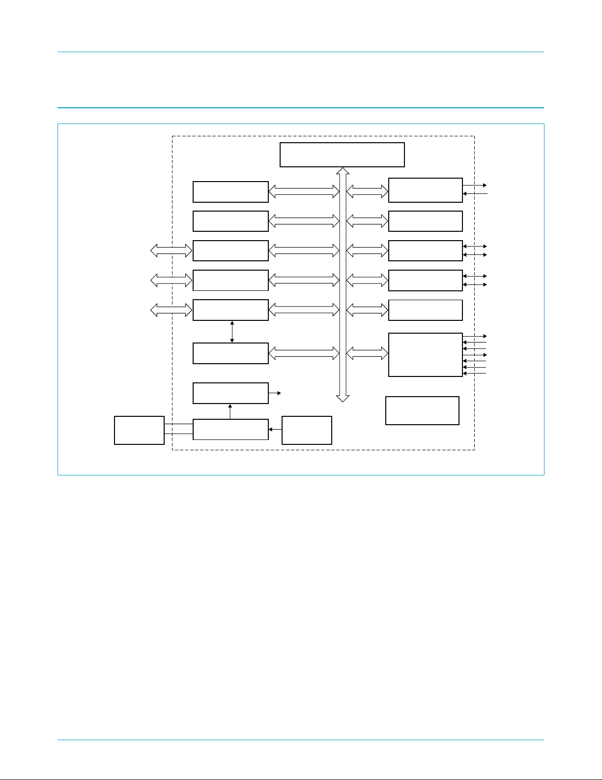
4. Block diagram
P89LPC920/921/922/9221
8-bit microcontrollers with two-clock 80C51 core
CRYSTAL
OR
RESONATOR
P89LPC920/921/922/9221
2 kB/4 kB/8 kB
CODE FLASH
256-BYTE
DATA RAM
PORT 3
CONFIGURABLE I/Os
PORT 1
CONFIGURABLE I/Os
PORT 0
CONFIGURABLE I/Os
KEYPAD
INTERRUPT
PROGRAMMABLE
OSCILLATOR DIVIDER
CONFIGURABLE
OSCILLATOR
HIGH PERFORMANCE
ACCELERATED 2-CLOCK 80C51 CPU
internal bus
CPU
clock
ON-CHIP
RC
OSCILLATOR
(POWER-ON RESET,
BROWNOUT RESET)
UART
REAL-TIME CLOCK/
SYSTEM TIMER
I2C
TIMER 0
TIMER 1
WATCHDOG TIMER
AND OSCILLATOR
ANALOG
COMPARATORS
POWER MONITOR
002aaa410
Fig 1. Block diagram.
9397 750 14469
Product data Rev. 08 — 15 December 2004 4 of 46
© Koninklijke Philips Electronics N.V. 2004. All rights reserved.

Philips Semiconductors
5. Pinning information
5.1 Pinning
P89LPC920/921/922/9221
8-bit microcontrollers with two-clock 80C51 core
handbook, halfpage
KBI0/CMP2/P0.0
P1.7
P1.6
RST/P1.5
V
SS
XTAL1/P3.1
CLKOUT/XTAL2/P3.0
INT1/P1.4
SDA/INT0/P1.3
SCL/T0/P1.2
Fig 2. TSSOP20 pin configuration.
handbook, halfpage
KBI0/CMP2/P0.0
P1.7
P1.6
RST/P1.5
V
SS
XTAL1/P3.1
CLKOUT/XTAL2/P3.0
INT1/P1.4
SDA/INT0/P1.3
SCL/T0/P1.2
1
2
3
4
5
6
7
P89LPC920FDH
8
9
10
1
2
3
4
5
6
7
8
9
10
P0.1/CIN2B/KBI1
20
P0.2/CIN2A/KBI2
19
P0.3/CIN1B/KBI3
18
P0.4/CIN1A/KBI4
17
P0.5/CMPREF/KBI5
16
V
15
DD
P0.6/CMP1/KBI6
14
P89LPC921FDH
P89LPC922FDH
P89LPC9221FDH
P0.7/T1/KBI7
13
P1.0/TXD
12
P1.1/RXD
11
002aaa408
P0.1/CIN2B/KBI1
20
P0.2/CIN2A/KBI2
19
P0.3/CIN1B/KBI3
18
P0.4/CIN1A/KBI4
17
P0.5/CMPREF/KBI5
16
V
15
DD
P0.6/CMP1/KBI6
14
P89LPC922FN
P89LPC9221FN
P0.7/T1/KBI7
13
P1.0/TXD
12
P1.1/RXD
11
002aaa407
Fig 3. DIP20 pin configuration.
9397 750 14469
Product data Rev. 08 — 15 December 2004 5 of 46
© Koninklijke Philips Electronics N.V. 2004. All rights reserved.

Philips Semiconductors
P89LPC920/921/922/9221
8-bit microcontrollers with two-clock 80C51 core
5.2 Pin description
Table 3: Pin description
Symbol Pin Type Description
P0.0 to P0.7 I/O Port 0: Port 0 is an 8-bit I/O port with a user-configurable output type. During reset
Port 0 latches are configured in the input only mode with the internal pull-up disabled.
The operation of Port 0 pins as inputs and outputs depends upon the port configuration
selected. Each port pin is configured independently. Refer to Section 8.12.1 “Port
configurations” and Table 8 “DC electrical characteristics” for details.
The Keypad Interrupt feature operates with Port 0 pins.
All pins have Schmitt triggered inputs.
Port 0 also provides various special functions as described below:
1 I/O P0.0 — Port 0 bit 0.
O CMP2 — Comparator 2 output.
I KBI0 — Keyboard input 0.
20 I/O P0.1 — Port 0 bit 1.
I CIN2B — Comparator 2 positive input B.
I KBI1 — Keyboard input 1.
19 I/O P0.2 — Port 0 bit 2.
I CIN2A — Comparator 2 positive input A.
I KBI2 — Keyboard input 2.
18 I/O P0.3 — Port 0 bit 3. High current source (P89LPC9221).
I CIN1B — Comparator 1 positive input B.
I KBI3 — Keyboard input 3.
17 I/O P0.4 — Port 0 bit 4. High current source (P89LPC9221).
I CIN1A — Comparator 1 positive input A.
I KBI4 — Keyboard input 4.
16 I/O P0.5 — Port 0 bit 5. High current source (P89LPC9221).
I CMPREF — Comparator reference (negative) input.
I KBI5 — Keyboard input 5.
14 I/O P0.6 — Port 0 bit 6. High current source (P89LPC9221).
O CMP1 — Comparator 1 output.
I KBI6 — Keyboard input 6.
13 I/O P0.7 — Port 0 bit 7. High current source (P89LPC9221).
I/O T1 — Timer/counter 1 external count input or overflow output.
I KBI7 — Keyboard input 7.
9397 750 14469
Product data Rev. 08 — 15 December 2004 6 of 46
© Koninklijke Philips Electronics N.V. 2004. All rights reserved.

Philips Semiconductors
P89LPC920/921/922/9221
8-bit microcontrollers with two-clock 80C51 core
Table 3: Pin description
…continued
Symbol Pin Type Description
P1.0 to P1.7 I/O, I
[1]
Port 1: Port 1 is an 8-bit I/O port with a user-configurable output type, except for three
pins as noted below. During reset Port 1 latches are configured in the input only mode
with the internal pull-up disabled. The operation of the configurablePort 1 pins as inputs
and outputs depends upon the port configuration selected. Each of the configurable
port pins are programmed independently. Refer to Section 8.12.1 “Port configurations”
and Table 8 “DC electrical characteristics” for details. P1.2 - P1.3 are open drain when
used as outputs. P1.5 is input only.
All pins have Schmitt triggered inputs.
Port 1 also provides various special functions as described below:
12 I/O P1.0 — Port 1 bit 0.
O TXD — Transmitter output for the serial port.
11 I/O P1.1 — Port 1 bit 1.
I RXD — Receiver input for the serial port.
10 I/O P1.2 — Port 1 bit 2 (open-drain when used as output).
I/O T0 — Timer/counter 0 external count input or overflowoutput (open-drain when used as
output).
I/O SCL — I
2
9 I/O P1.3 — Port 1 bit 3 (open-drain when used as output).
I
I/O SDA — I
INT0 — External interrupt 0 input.
2
8 I/O P1.4 — Port 1 bit 4. High current source (P89LPC9221).
I
INT1 — External interrupt 1 input.
4IP1.5 — Port 1 bit 5 (input only).
I
RST — External Reset input (if selected via FLASH configuration). A LOW on this pin
resets the microcontroller, causing I/O ports and peripherals to take on their default
states, and the processor begins execution at address 0. When using an oscillator
frequency above 12 MHz, the reset input function of P1.5 must be enabled. An
external circuit is required to hold the device in reset at power-up until V
reached its specified level. When system power is removed V
minimum specified operating voltage. When using an oscillator frequency above
12 MHz, in some applications, an external brownout detect circuit may be
required to hold the device in reset when V
operating voltage.
3 I/O P1.6 — Port 1 bit 6. High current source (P89LPC9221).
2 I/O P1.7 — Port 1 bit 7. High current source (P89LPC9221).
C serial clock input/output.
C serial data input/output.
will fall below the
DD
falls below the minimum specified
DD
DD
has
9397 750 14469
Product data Rev. 08 — 15 December 2004 7 of 46
© Koninklijke Philips Electronics N.V. 2004. All rights reserved.
Philips Semiconductors
P89LPC920/921/922/9221
8-bit microcontrollers with two-clock 80C51 core
Table 3: Pin description
…continued
Symbol Pin Type Description
P3.0 to P3.1 I/O Port 3: Port 3 is an 2-bit I/O port with a user-configurable output type. During reset
Port 3 latches are configured in the input only mode with the internal pull-up disabled.
The operation of Port 3 pins as inputs and outputs depends upon the port configuration
selected. Each port pin is configured independently. Refer to Section 8.12.1 “Port
configurations” and Table 8 “DC electrical characteristics” for details.
All pins have Schmitt triggered inputs.
Port 3 also provides various special functions as described below:
7 I/O P3.0 — Port 3 bit 0.
O XTAL2 — Output from the oscillator amplifier (when a crystal oscillator option is
selected via the FLASH configuration.
O CLKOUT — CPU clock divided by 2 when enabled via SFR bit (ENCLK - TRIM.6). It
can be used if the CPU clock is the internal RC oscillator, watchdog oscillator or
external clock input, except when XTAL1/XTAL2 are used to generate clock source for
the real time clock/system timer.
6 I/O P3.1 — Port 3 bit 1.
I XTAL1 — Input to the oscillator circuit and internal clock generator circuits (when
selected via the FLASH configuration). It can be a port pin if internal RC oscillator or
watchdog oscillator is used as the CPU clock source, and if XTAL1/XTAL2 are not used
to generate the clock for the real time clock/system timer.
V
SS
V
DD
5IGround: 0 V reference.
15 I Power Supply: This is the power supply voltage for normal operation as well as Idle
and Power down modes.
[1] Input/Output for P1.0-P1.4, P1.6, P1.7. Input for P1.5.
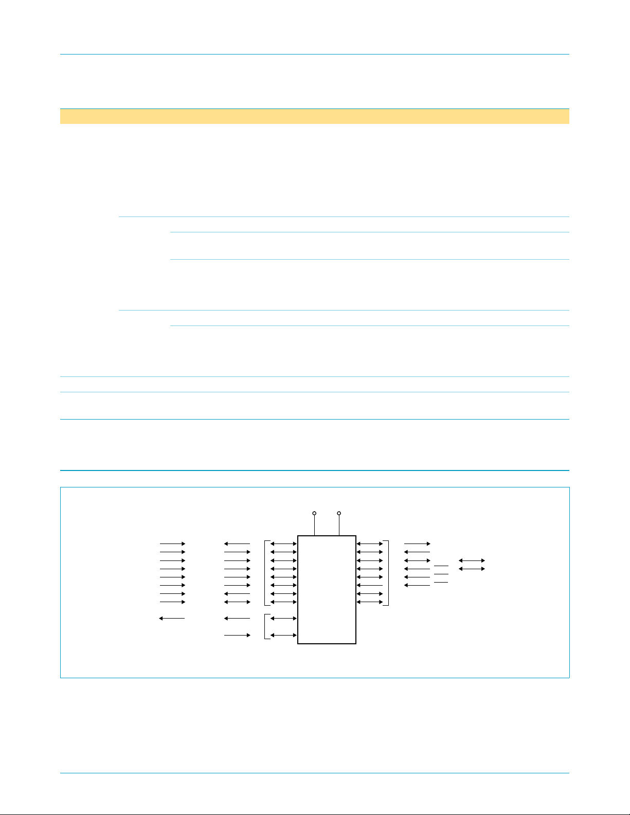
6. Logic symbol
KBI0
KBI1
KBI2
KBI3
KBI4
KBI5
KBI6
KBI7
CLKOUT
Fig 4. Logic symbol.
CMP2
CIN2B
CIN2A
CIN1B
CIN1A
CMPREF
CMP1
T1
XTAL2
XTAL1
PORT 0
PORT 3
V
DDVSS
P89LPC920/921/922/9221
002aaa409
PORT 1
TxD
RxD
T0
INT0
INT1
RST
SCL
SDA
9397 750 14469
Product data Rev. 08 — 15 December 2004 8 of 46
© Koninklijke Philips Electronics N.V. 2004. All rights reserved.

Philips Semiconductors
7. Special function registers
Remark: Special Function Registers (SFRs) accesses are restricted in the following
ways:
• User must not attempt to access any SFR locations not defined.
• Accesses to any defined SFR locations must be strictly for the functions for the
SFRs.
• SFR bits labeled ‘-’, ‘0’ or ‘1’ can only be written and read as follows:
– ‘-’ Unless otherwise specified, must be written with ‘0’, but can return any value
when read (even if it was written with ‘0’). It is a reserved bit and may be used in
future derivatives.
– ‘0’ must be written with ‘0’, and will return a ‘0’ when read.
– ‘1’ must be written with ‘1’, and will return a ‘1’ when read.
P89LPC920/921/922/9221
8-bit microcontrollers with two-clock 80C51 core
9397 750 14469
Product data Rev. 08 — 15 December 2004 9 of 46
© Koninklijke Philips Electronics N.V. 2004. All rights reserved.

xxxxxxxxxxxxxxxxxxxxx xxxxxxxxxxxxxxxxxxxxxxxxxx xxxxxxx x x x xxxxxxxxxxxxxxxxxxxxxxxxxxxxxx xxxxxxxxxxxxxxxxxxx xx xx
xxxxx xxxxxxxxxxxxxxxxxxxxxxxxxxx xxxxxxxxxxxxxxxxxxx xxxxxx xxxxxxxxxxxxxxxxxxxxxxxxxxxxxxxxxxx xxxxxxxxxxxx x x
xxxxxxxxxxxxxxxxxxxxx xxxxxxxxxxxxxxxxxxxxxxxxxxxxxx xxxxx xxxxxxxxxxxxxxxxxxxxxxxxxxxxxxxxxxxxxxxxxxxxxxxxxx xxxxxxxx
9397 750 14469
Product data Rev. 08 — 15 December 2004 10 of 46
Table 4: Special function registers
* indicates SFRs that are bit addressable.
Name Description SFR
ACC* Accumulator E0H 00 00000000
AUXR1 Auxiliary function register A2H CLKLP EBRR ENT1 ENT0 SRST 0 - DPS 00
B* B register F0H 00 00000000
BRGR0
BRGR1
BRGCON Baud rate generator control BDH - - - - - - SBRGS BRGEN 00 xxxxxx00
CMP1 Comparator 1 control register ACH - - CE1 CP1 CN1 OE1 CO1 CMF1 00
CMP2 Comparator 2 control register ADH - - CE2 CP2 CN2 OE2 CO2 CMF2 00
DIVM CPU clock divide-by-M
DPTR Data pointer (2 bytes)
DPH Data pointer HIGH 83H 00 00000000
DPL Data pointer LOW 82H 00 00000000
FMADRH Program Flash address HIGH E7H 00 00000000
FMADRL Program Flash address LOW E6H 00 00000000
FMCON Program Flash control (Read) E4H BUSY - - - HVA HVE SV OI 70 01110000
© Koninklijke Philips Electronics N.V. 2004. All rights reserved.
FMDATA Program Flash data E5H 00 00000000
I2ADR I
I2CON* I
I2DAT I
I2SCLH Serial clock generator/SCL
xxxxxxxxxxxxxxxxxxxxxxxxx xxxxxxxxxxxxxxxxxxxx xxx
Bit functions and addresses Reset value
addr.
Bit address E7 E6 E5 E4 E3 E2 E1 E0
Bit address F7 F6 F5 F4 F3 F2 F1 F0
[2]
Baud rate generator rate
BEH 00 00000000
LOW
[2]
Baud rate generator rate
BFH 00 00000000
HIGH
95H 00 00000000
control
Program Flash control (Write) E4H FMCMD.7FMCMD.6FMCMD.5FMCMD.4FMCMD.3FMCMD.2FMCMD.1FMCMD.
2
C slave address register DBH I2ADR.6 I2ADR.5 I2ADR.4 I2ADR.3 I2ADR.2 I2ADR.1 I2ADR.0 GC 00 00000000
Bit address DF DE DD DC DB DA D9 D8
2
C control register D8H - I2EN STA STO SI AA - CRSEL 00 x00000x0
2
C data register DAH
DDH 00 00000000
duty cycle register HIGH
MSB LSB Hex Binary
[1]
[1]
[1]
0
000000x0
xx000000
xx000000
Philips Semiconductors
P89LPC920/921/922/9221
8-bit microcontrollers with two-clock 80C51 core

xxxxxxxxxxxxxxxxxxxxx xxxxxxxxxxxxxxxxxxxxxxxxxx xxxxxxx x x x xxxxxxxxxxxxxxxxxxxxxxxxxxxxxx xxxxxxxxxxxxxxxxxxx xx xx
xxxxx xxxxxxxxxxxxxxxxxxxxxxxxxxx xxxxxxxxxxxxxxxxxxx xxxxxx xxxxxxxxxxxxxxxxxxxxxxxxxxxxxxxxxxx xxxxxxxxxxxx x x
xxxxxxxxxxxxxxxxxxxxx xxxxxxxxxxxxxxxxxxxxxxxxxxxxxx xxxxx xxxxxxxxxxxxxxxxxxxxxxxxxxxxxxxxxxxxxxxxxxxxxxxxxx xxxxxxxx
9397 750 14469
Product data Rev. 08 — 15 December 2004 11 of 46
Table 4: Special function registers
* indicates SFRs that are bit addressable.
Name Description SFR
I2SCLL Serial clock generator/SCL
I2STAT I
IEN0* Interrupt enable 0 A8H EA EWDRT EBO ES/ESR ET1 EX1 ET0 EX0 00
IEN1* Interrupt enable 1 E8H - EST - - - EC EKBI EI2C 00
IP0* Interrupt priority 0 B8H - PWDRT PBO PS/PSR PT1 PX1 PT0 PX0 00
IP0H Interrupt priority 0 HIGH B7H - PWDRTHPBOH PSH/
IP1* Interrupt priority 1 F8H - PST - - - PC PKBI PI2C 00
IP1H Interrupt priority 1 HIGH F7H - PSTH - - - PCH PKBIH PI2CH 00
KBCON Keypad control register 94H - - - - - - PATN
KBMASK Keypad interrupt mask
KBPATN Keypad pattern register 93H FF 11111111
P0* Port 0 80H T1/KB7 CMP1
© Koninklijke Philips Electronics N.V. 2004. All rights reserved.
P1* Port 1 90H - -
P3* Port 3 B0H - - - - - - XTAL1 XTAL2
P0M1 Port 0 output mode 1 84H (P0M1.7) (P0M1.6) (P0M1.5) (P0M1.4) (P0M1.3) (P0M1.2) (P0M1.1) (P0M1.0) FF 11111111
P0M2 Port 0 output mode 2 85H (P0M2.7) (P0M2.6) (P0M2.5) (P0M2.4) (P0M2.3) (P0M2.2) (P0M2.1) (P0M2.0) 00 00000000
P1M1 Port 1 output mode 1 91H (P1M1.7) (P1M1.6) - (P1M1.4) (P1M1.3) (P1M1.2) (P1M1.1) (P1M1.0) D3
xxxxxxxxxxxxxxxxxxxxxxxxx xxxxxxxxxxxxxxxxxxxx xxx
…continued
Bit functions and addresses Reset value
addr.
DCH 00 00000000
duty cycle register LOW
2
C status register D9H STA.4 STA.3 STA.2 STA.1 STA.0 0 0 0 F8 11111000
Bit address AF AE AD AC AB AA A9 A8
Bit address EF EE ED EC EB EA E9 E8
Bit address BF BE BD BC BB BA B9 B8
Bit address FF FE FD FC FB FA F9 F8
86H 00 00000000
register
Bit address 87 86 85 84 83 82 81 80
Bit address 97 96 95 94 93 92 91 90
Bit address B7 B6 B5 B4 B3 B2 B1 B0
MSB LSB Hex Binary
[1]
[1]
[1]
PT1H PX1H PT0H PX0H 00
[1]
PSRH
[1]
[1]
KBIF 00
[1]
_SEL
/KB6
CMPREF
/KB5
RST INT1 INT0/
CIN1A
/KB4
CIN1B
/KB3
CIN2A
/KB2
CIN2B
/KB1
CMP2
/KB0
T0/SCL RXD TXD
SDA
[1]
00000000
00x00000
x0000000
x0000000
00x00000
00x00000
xxxxxx00
[1]
[1]
[1]
11x1xx11
Philips Semiconductors
P89LPC920/921/922/9221
8-bit microcontrollers with two-clock 80C51 core

xxxxxxxxxxxxxxxxxxxxx xxxxxxxxxxxxxxxxxxxxxxxxxx xxxxxxx x x x xxxxxxxxxxxxxxxxxxxxxxxxxxxxxx xxxxxxxxxxxxxxxxxxx xx xx
xxxxx xxxxxxxxxxxxxxxxxxxxxxxxxxx xxxxxxxxxxxxxxxxxxx xxxxxx xxxxxxxxxxxxxxxxxxxxxxxxxxxxxxxxxxx xxxxxxxxxxxx x x
xxxxxxxxxxxxxxxxxxxxx xxxxxxxxxxxxxxxxxxxxxxxxxxxxxx xxxxx xxxxxxxxxxxxxxxxxxxxxxxxxxxxxxxxxxxxxxxxxxxxxxxxxx xxxxxxxx
9397 750 14469
Product data Rev. 08 — 15 December 2004 12 of 46
Table 4: Special function registers
* indicates SFRs that are bit addressable.
Name Description SFR
P1M2 Port 1 output mode 2 92H (P1M2.7) (P1M2.6) - (P1M2.4) (P1M2.3) (P1M2.2) (P1M2.1) (P1M2.0) 00
P3M1 Port 3 output mode 1 B1H - - - - - - (P3M1.1) (P3M1.0) 03
P3M2 Port 3 output mode 2 B2H - - - - - - (P3M2.1) (P3M2.0) 00
PCON Power control register 87H SMOD1 SMOD0 BOPD BOI GF1 GF0 PMOD1 PMOD0 00 00000000
PCONA Power control register A B5H RTCPD - VCPD - I2PD - SPD - 00
PSW* Program status word D0H CY AC F0 RS1 RS0 OV F1 P 00H 00000000
PT0AD Port 0 digital input disable F6H - - PT0AD.5 PT0AD.4 PT0AD.3 PT0AD.2 PT0AD.1 - 00H xx00000x
RSTSRC Reset source register DFH - - BOF POF R_BK R_WD R_SF R_EX
RTCCON Real-time clock control D1H RTCF RTCS1 RTCS0 - - - ERTC RTCEN 60
RTCH Real-time clock register
RTCL Real-time clock register LOW D3H 00
SADDR Serial port address register A9H 00 00000000
SADEN Serial port address enable B9H 00 00000000
SBUF Serial Port data buffer
SCON* Serial port control 98H SM0/FE SM1 SM2 REN TB8 RB8 TI RI 00 00000000
SSTAT Serial port extended status
© Koninklijke Philips Electronics N.V. 2004. All rights reserved.
SP Stack pointer 81H 07 00000111
TAMOD Timer 0 and 1 auxiliary mode 8FH - - - T1M2 - - - T0M2 00 xxx0xxx0
TCON* Timer 0 and 1 control 88H TF1 TR1 TF0 TR0 IE1 IT1 IE0 IT0 00 00000000
TH0 Timer 0 HIGH 8CH 00 00000000
TH1 Timer 1 HIGH 8DH 00 00000000
TL0 Timer 0 LOW 8AH 00 00000000
TL1 Timer 1 LOW 8BH 00 00000000
TMOD Timer 0 and 1 mode 89H T1GATE T1C/T T1M1 T1M0 T0GATE T0C/T T0M1 T0M0 00 00000000
xxxxxxxxxxxxxxxxxxxxxxxxx xxxxxxxxxxxxxxxxxxxx xxx
…continued
Bit functions and addresses Reset value
addr.
Bit address D7 D6 D5 D4 D3 D2 D1 D0
D2H 00
HIGH
99H xx xxxxxxxx
register
Bit address 9F 9E 9D 9C 9B 9A 99 98
BAH DBMOD INTLO CIDIS DBISEL FE BR OE STINT 00 00000000
register
Bit address 8F 8E 8D 8C 8B 8A 89 88
MSB LSB Hex Binary
[1]
[1]
[1]
[1]
[1][6]
[6]
[6]
00x0xx00
xxxxxx11
xxxxxx00
00000000
[3]
00000000
00000000
Philips Semiconductors
P89LPC920/921/922/9221
8-bit microcontrollers with two-clock 80C51 core

xxxxxxxxxxxxxxxxxxxxx xxxxxxxxxxxxxxxxxxxxxxxxxx xxxxxxx x x x xxxxxxxxxxxxxxxxxxxxxxxxxxxxxx xxxxxxxxxxxxxxxxxxx xx xx
xxxxx xxxxxxxxxxxxxxxxxxxxxxxxxxx xxxxxxxxxxxxxxxxxxx xxxxxx xxxxxxxxxxxxxxxxxxxxxxxxxxxxxxxxxxx xxxxxxxxxxxx x x
xxxxxxxxxxxxxxxxxxxxx xxxxxxxxxxxxxxxxxxxxxxxxxxxxxx xxxxx xxxxxxxxxxxxxxxxxxxxxxxxxxxxxxxxxxxxxxxxxxxxxxxxxx xxxxxxxx
9397 750 14469
Product data Rev. 08 — 15 December 2004 13 of 46
Table 4: Special function registers
* indicates SFRs that are bit addressable.
Name Description SFR
TRIM Internal oscillator trim register 96H - ENCLK TRIM.5 TRIM.4 TRIM.3 TRIM.2 TRIM.1 TRIM.0
WDCON Watchdog control register A7H PRE2 PRE1 PRE0 - - WDRUN WDTOF WDCLK
WDL Watchdog load C1H FF 11111111
WFEED1 Watchdog feed 1 C2H
WFEED2 Watchdog feed 2 C3H
[1] All ports are in input only (high impedance) state after power-up.
[2] BRGR1 and BRGR0 must only be written if BRGEN in BRGCON SFR is ‘0’. If any are written while BRGEN = 1, the result is unpredictable.
[3] The RSTSRC register reflects the cause of the P89LPC920/921/922/9221 reset. Upon a power-up reset, all reset source flags are cleared except POF and BOF; the power-on
[4] After reset, the valueis 111001x1, i.e., PRE2-PRE0 are all ‘1’, WDRUN = 1 and WDCLK = 1. WDTOF bit is ‘1’ after watchdogreset and is ‘0’ after power-on reset. Other resets will
[5] On power-on reset, the TRIM SFR is initialized with a factory preprogrammed value. Other resets will not cause initialization of the TRIM register.
[6] The only reset source that affects these SFRs is power-on reset.
xxxxxxxxxxxxxxxxxxxxxxxxx xxxxxxxxxxxxxxxxxxxx xxx
…continued
Bit functions and addresses Reset value
addr.
reset value is xx110000.
not affect WDTOF.
MSB LSB Hex Binary
Philips Semiconductors
[5] [6]
[4] [6]
P89LPC920/921/922/9221
8-bit microcontrollers with two-clock 80C51 core
© Koninklijke Philips Electronics N.V. 2004. All rights reserved.

Philips Semiconductors
8. Functional description
P89LPC920/921/922/9221
8-bit microcontrollers with two-clock 80C51 core
Remark: Please refer to the
detailed functional description.
8.1 Enhanced CPU
The P89LPC920/921/922/9221 uses an enhanced 80C51 CPU which runs at 6 times
the speed of standard 80C51 devices. A machine cycle consists of two CPU clock
cycles, and most instructions execute in one or two machine cycles.
8.2 Clocks
8.2.1 Clock definitions
The P89LPC920/921/922/9221 device has several internal clocks as defined below:
OSCCLK — Input to the DIVM clock divider. OSCCLK is selected from one of four
clock sources (see Figure 5) and can also be optionally divided to a slower frequency
(see Section 8.7 “CPU Clock (CCLK) modification: DIVM register”).
Note: f
CCLK — CPU clock; output of the clock divider. There are two CCLK cycles per
machine cycle, and most instructions are executed in one to two machine cycles (two
or four CCLK cycles).
RCCLK — The internal 7.373 MHz RC oscillator output.
PCLK — Clock for the various peripheral devices and is CCLK/2
is defined as the OSCCLK frequency.
osc
P89LPC920/921/922/9221 User’s Manual
for a more
8.2.2 CPU clock (OSCCLK)
The P89LPC920/921/922/9221 provides several user-selectable oscillator options in
generating the CPU clock. This allows optimization for a range of needs from high
precision to lowest possible cost. These options are configured when the FLASH is
programmed and include an on-chip watchdog oscillator, an on-chip RC oscillator, an
oscillator using an external crystal, or an external clock source. The crystal oscillator
can be optimized for low, medium, or high frequency crystals covering a range from
20 kHz to 12 MHz.
8.2.3 Low speed oscillator option
This option supports an external crystal in the range of 20 kHz to 100 kHz. Ceramic
resonators are also supported in this configuration.
8.2.4 Medium speed oscillator option
This option supports an external crystal in the range of 100 kHz to 4 MHz. Ceramic
resonators are also supported in this configuration.
8.2.5 High speed oscillator option
This option supports an external crystal in the range of 4 MHz to 18 MHz. Ceramic
resonators are also supported in this configuration. When using an oscillator
frequency above 12 MHz, the reset input function of P1.5 must be enabled. An
external circuit is required to hold the device in reset at power-up until VDDhas
reached its specified level. When system power is removed VDD will fall below
9397 750 14469
Product data Rev. 08 — 15 December 2004 14 of 46
© Koninklijke Philips Electronics N.V. 2004. All rights reserved.
 Loading...