Philips p89c738 DATASHEETS

INTEGRATED CIRCUITS
DATA SH EET
P89C738; P89C739
8-bit microcontrollers
Product specification
File under Integrated Circuits, IC20
1997 Dec 15

Philips Semiconductors Product specification
8-bit microcontrollers P89C738; P89C739
CONTENTS
1 FEATURES
2 GENERAL DESCRIPTION
3 ORDERING INFORMATION
4 BLOCK DIAGRAM
5 FUNCTIONAL DIAGRAM
6 PINNING INFORMATION
6.1 Pin configuration
6.2 Pin description
7 FUNCTIONAL DESCRIPTION
7.1 General
7.2 Instruction set execution
8 MEMORY ORGANIZATION
8.1 Program memory
8.2 Internal data memory
8.3 Addressing
9 INTERRUPT SYSTEM
9.1 Interrupt Enable Register (IE)
9.2 Interrupt Priority Register (IP)
10 TIMERS/COUNTERS
10.1 Timer 0 and Timer 1
10.2 Timer 2
10.3 Watchdog Timer (T3)
11 I/O FACILITIES
12 FULL DUPLEX SERIAL PORT (UART)
12.1 The Serial Port operating modes
12.2 Serial Port Control Register (SCON)
13 REDUCED POWER MODES
13.1 Idle mode
13.2 Power-down mode
13.3 Wake-up from Power-down mode
13.4 Status of external pins
13.5 Power Control Register (PCON)
14 OSCILLATOR CIRCUIT
15 RESET
15.1 Power-on reset
16 MULTIPLE PROGRAMMING ROM
(MTP-ROM)
16.1 Features
16.2 General description
16.3 Automatic programming and Automatic chip
erase
16.4 Command definitions
16.5 Silicon-ID-Read command
16.6 Set-up of Automatic chip erase and Automatic
erase commands
16.7 Set-up of the Automatic program and Program
commands
16.8 Reset command
16.9 Write operation status
16.10 Write operation
16.11 System considerations
16.12 Command programming/data programming
and erase operation
17 SPECIAL FUNCTION REGISTERS
OVERVIEW
18 INSTRUCTION SET
19 LIMITING VALUES
20 DC CHARACTERISTICS
21 AC CHARACTERISTICS
21.1 Serial Port characteristics
21.2 Timing waveforms
21.3 Timing symbol naming conventions
22 PACKAGE OUTLINES
23 SOLDERING
23.1 Introduction
23.2 DIP
23.3 PLCC and QFP
24 DEFINITIONS
25 LIFE SUPPORT APPLICATIONS
1997 Dec 15 2

Philips Semiconductors Product specification
8-bit microcontrollers P89C738; P89C739
1 FEATURES
• 80C51 CPU
• 64 kbytes on-chip Multiple Programming ROM
(MTP-ROM), expandable externally to 64 kbytes
program memory address space
• 512 bytes on-chip RAM, expandable externally to
64 kbytes data memory address space
• P89C738 pin outs fully compatible to the standard
8051/8052
• 8-bit I/O ports for P89C738: 4 and P89C739: 6
• Full-duplex UART compatible with the standard 80C51
and the 8052
• Two standard 16-bit timers/event counters
• An additional 16-bit timer (functionally equivalent to the
Timer 2 of the 8052)
• On-chip Watchdog Timer (T3)
• 6-source and 6-vector interrupt structure with 2 priority
levels
• Up to 3 external interrupt request inputs
• Two programmable power reduction modes: Idle and
Power-down
• Termination of Idle mode by any interrupt, external or
Watchdog Timer reset
• Wake-up from Power-down by external interrupt,
external or Watchdog Timer reset
• Packages,
– P89C738: DIP40, PLCC44 and QFP44
– P89C739: PLCC68 and QFP64
• Improved Electromagnetic Compatibility (EMC)
• Frequency range: 3.5 to 40 MHz
• ROM code protection
2 GENERAL DESCRIPTION
The P89C738 and P89C739 (hereafter generally referred
to as P89C738 unless the P89C739 is specifically
mentioned) are 8-bit microcontrollers manufactured in an
advanced CMOS process and is a derivative of the
PCB80C51 microcontroller family. This device provides
architectural enhancements that make it applicable in a
variety of applications in general control systems,
especially in those systems which need a large on-chip
ROM and RAM capacity.
The P89C738 contains a non-volatile 64 kbytes Multiple
Programming ROM (MTP-ROM) program memory, a
volatile 512 bytes read/write data memory, four 8-bit I/O
ports (six for the P89C739), two 16-bit timer/event
counters (identical to the timers of the 80C51), a 16-bit
timer (identical to the Timer 2 of the 8052), a multi-source
two-priority-level nested interrupt structure, one serial
interface (UART), a Watchdog Timer (T3), an on-chip
oscillator and timing circuits. For systems that require
extra capability, the P89C738 can be expanded using
standard TTL compatible memories and logic.
The device also functions as an arithmetic processor
having facilities for both binary and BCD arithmetic plus
bit-handling capabilities. The P89C738 has the same
instruction set as the PCB80C51 which consists of over
100 instructions: 49 one-byte, 46 two-byte and
16 three-byte. With a 16 MHz crystal, 58% of the
instructions are executed in 750 ns and 40% in 1.5 µs.
Multiply and divide instructions require 3 µs.
3 ORDERING INFORMATION
TYPE
NUMBER
P89C738ABA PLCC44 plastic leaded chip carrier; 44 leads note 2
P89C738ABP DIP40 plastic dual in-line package; 40 leads (600 mil) SOT129-1
P89C738BBB QFP44 plastic quad flat package; 44 leads note 2
P89C739ABA PLCC68 plastic leaded chip carrier; 68 leads note 2
P89C739ABB QFP64 plastic quad flat package; 64 leads (lead length 1.95 mm);
Note
1. Temperature and frequency range for all types: 0 to 70 °C and 3.5 to 40 MHz.
2. For more information on the package outline of this version, please contact the Philips Semiconductors Sales office.
1997 Dec 15 3
(1)
NAME DESCRIPTION VERSION
body 14 × 20 × 2.7 mm; high stand-off height
PACKAGE
SOT319-1
Philips Semiconductors Product specification
8-bit microcontrollers P89C738; P89C739
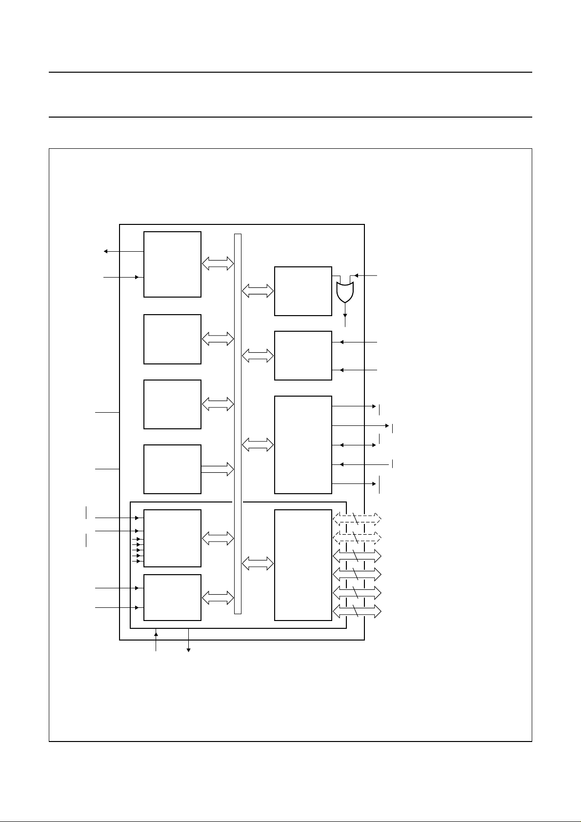
4 BLOCK DIAGRAM
SS
V
book, full pagewidth
DD
V
(2)
INT1
(2)
INT0
(2)
T1
(2)
T0
(2)
TXD
(2)
RXD
internal
interrupts
UART
SHIFT
SERIAL PORT
FULL DUPLEX
PROGRAMMABLE
TWO 16-BIT
SYNCHRONOUS
DATA
256 bytes
MEMORY
AUX-RAM
RAM
DATA
256 bytes
MEMORY
64 kbytes
MEMORY
PROGRAM
CPU
EVENT
TIMERS/
COUNTERS
MTP-ROM
(T0, T1)
P89C738
P89C739
excluding
ROM/RAM
80C51 core
8-bit
internal bus
(T3)
TIMER
WATCHDOG
16-BIT
(T2)
EVENT
TIMER/
COUNTER
16 kbytes BUS
EXPANSION CONTROL
AND
EXTERNAL BUS
PARALLEL I/O PORTS
reset
internal
888888
RST
(1)
T2
(1)
T2EX
(2)
ALE/WE WR
PSEN
(3)
P5
(3)
P4
P3P2P1P0
MGK189
(2)
RD
EA
Fig.1 Block diagram.
XTAL1
XTAL2
1997 Dec 15 4
(1) Alternative function for Port 1.
(2) Alternative function for Port 3.
(3) P4 and P5 are only available on the P89C738ABA and P89C739ABB (PLCC68 and QFP64).
Philips Semiconductors Product specification
8-bit microcontrollers P89C738; P89C739
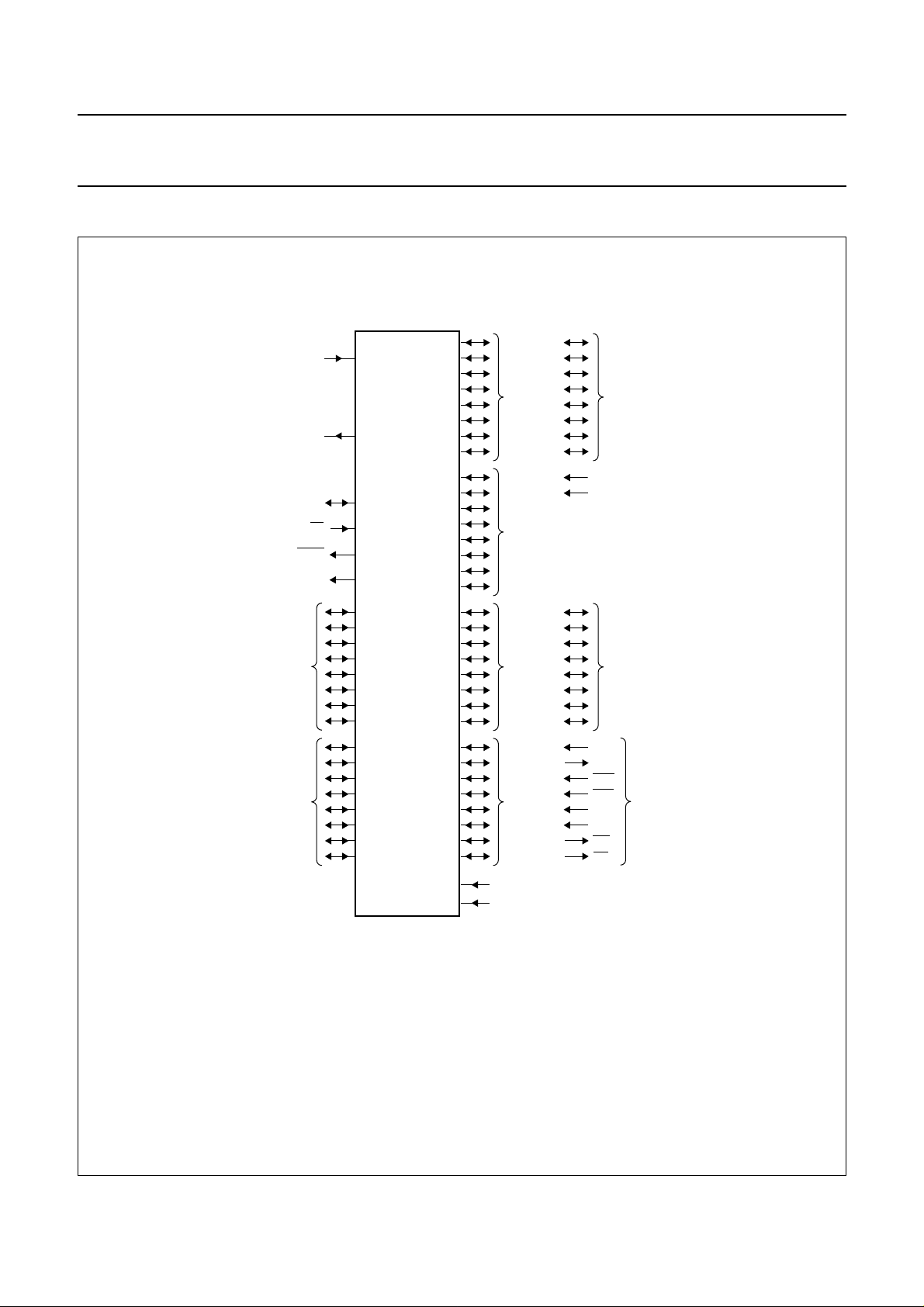
5 FUNCTIONAL DIAGRAM
handbook, full pagewidth
XTAL1
XTAL2
PORT 5
PORT 4
RST
EA
PSEN
ALE
P89C738
P89C739
PORT 0
PORT 1
PORT 2
PORT 3
T2
T2EX
RXD
TXD
INT0
INT1
T0
T1
WR
RD
ADDRESS
AND
DATA BUS
ADDRESS
BUS
secondary
functions
MGK191
Fig.2 Functional diagram.
1997 Dec 15 5
V
SS
V
DD
Philips Semiconductors Product specification
8-bit microcontrollers P89C738; P89C739
6 PINNING INFORMATION
6.1 Pin configuration
handbook, full pagewidth
P1.5
P1.6
P1.7
RST
P3.0/RXD/data
n.c.
P3.1/TXD/clock
P3.2/INT0
P3.3/INT1
P3.4/T0
P3.5/T1
V
XTAL1
41
40
P89C738ABA
15
16
P1.2
P1.0/T2
P1.1/T2EX
SS
XTAL2
P3.7/RD
P3.6/WR
44
43
42
1
2
3
4
5
6
7
8
9
10
11
12
13
14
P1.4
P1.3
n.c.
39
17
n.c.
P2.1/A9
P2.0/A8
38
37
18
19
DD
V
P0.0/AD0
P2.2/A10
P2.3/A11
36
35
21
20
P0.1/AD1
P0.2/AD2
P2.4/A12
34
22
MGK186
P0.3/AD3
33
32
31
30
29
28
27
26
25
24
23
P0.4/AD4
P0.5/AD5
P0.6/AD6
P0.7/AD7
EA/V
PP
n.c.
ALE/WE
PSEN
P2.7/A15
P2.6/A14
P2.5/A13
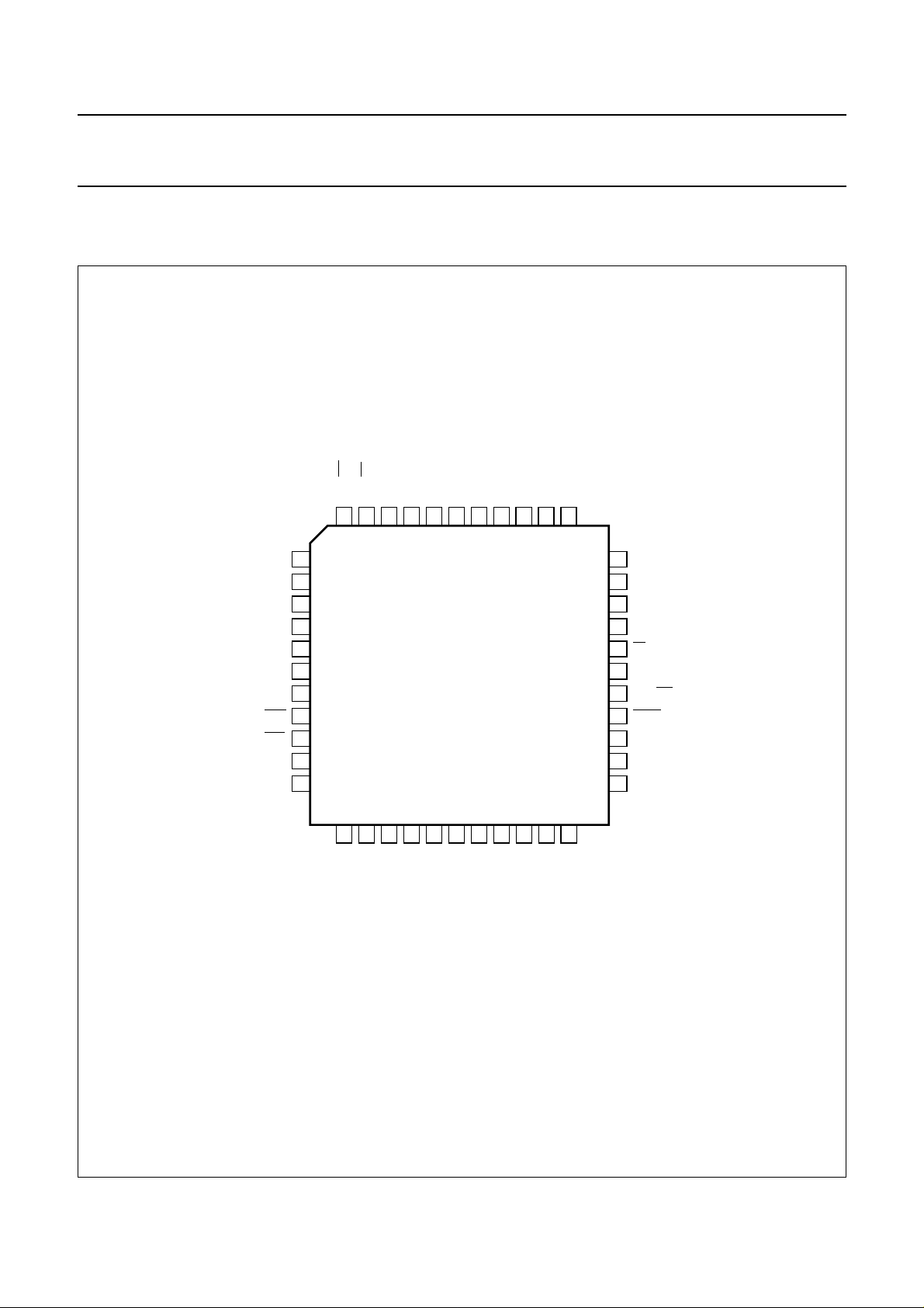
Fig.3 Pin configuration for PLCC44 package; for more information on the version see Chapter 3.
1997 Dec 15 6
Philips Semiconductors Product specification
8-bit microcontrollers P89C738; P89C739
handbook, halfpage
P1.0/T2
P1.1/T2EX
P3.0/RXD/data
P3.1/TXD/clock
P3.2/INT0
P3.3/INT1
P3.4/T0
P3.5/T1
P3.6/WR
P3.7/RD
P1.2
P1.3
P1.4
P1.5
P1.6
P1.7
RST
XTAL2
XTAL1
V
SS
1
2
3
4
5
6
7
8
9
10
P89C738ABP
11
12
13
14
15
16
17
18
19
20
MGK184
40
39
38
37
36
35
34
33
32
31
30
29
28
27
26
25
24
23
22
21
V
DD
P0.0/AD0
P0.1/AD1
P0.2/AD2
P0.3/AD3
P0.4/AD4
P0.5/AD5
P0.6/AD6
P0.7/AD7
EA/V
PP
ALE/WE
PSEN
P2.7/A15
P2.6/A14
P2.5/A13
P2.4/A12
P2.3/A11
P2.2/A10
P2.1/A9
P2.0/A8
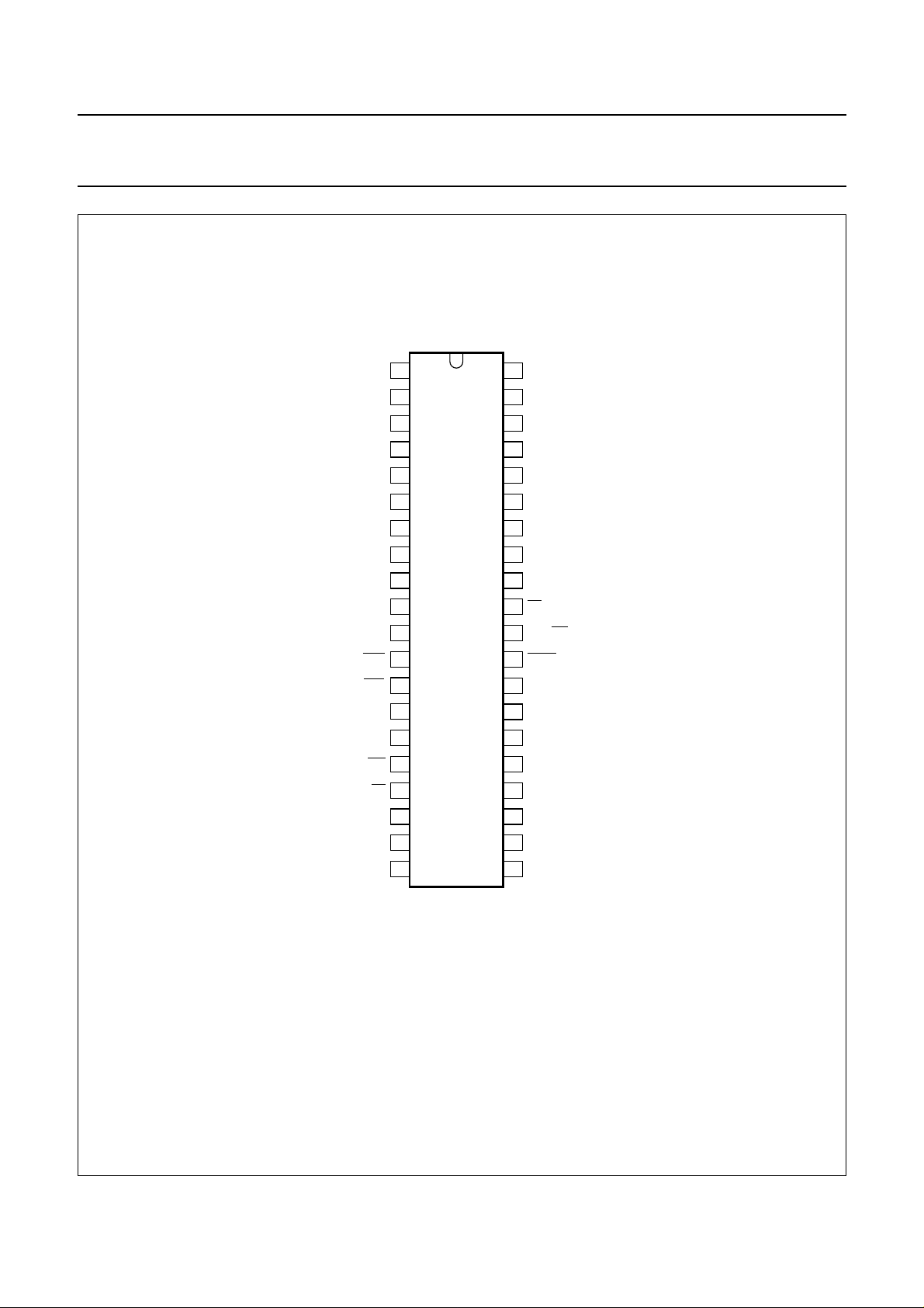
Fig.4 Pin configuration for DIP40 package (SOT129-1).
1997 Dec 15 7
Philips Semiconductors Product specification
8-bit microcontrollers P89C738; P89C739
handbook, full pagewidth
P1.5
P1.6
P1.7
RST
P3.0/RXD/data
n.c.
P3.1/TXD/clock
P3.2/INT0
P3.3/INT1
P3.4/T0
P3.5/T1
P1.4
P1.3
P1.2
P1.1/T2EX
6
5
4
3
7
8
9
10
11
12
13
14
15
16
17
18
19
P3.6/WR
20
XTAL2
P3.7/RD
P89C738BBB
21
XTAL1
P1.0/T2
n.c.
2
1
22
23
SS
n.c.
V
VDDP0.0/AD0
44
43
24
25
P2.0/A8
P2.1/A9
P0.1/AD1
P0.2/AD2
42
41
27
26
P2.2/A10
P2.3/A11
P0.3/AD3
40
28
MGK185
P2.4/A12
39
38
37
36
35
34
33
32
31
30
29
P0.4/AD4
P0.5/AD5
P0.6/AD6
P0.7/AD7
EA/V
PP
n.c.
ALE/WE
PSEN
P2.7/A15
P2.6/A14
P2.5/A13
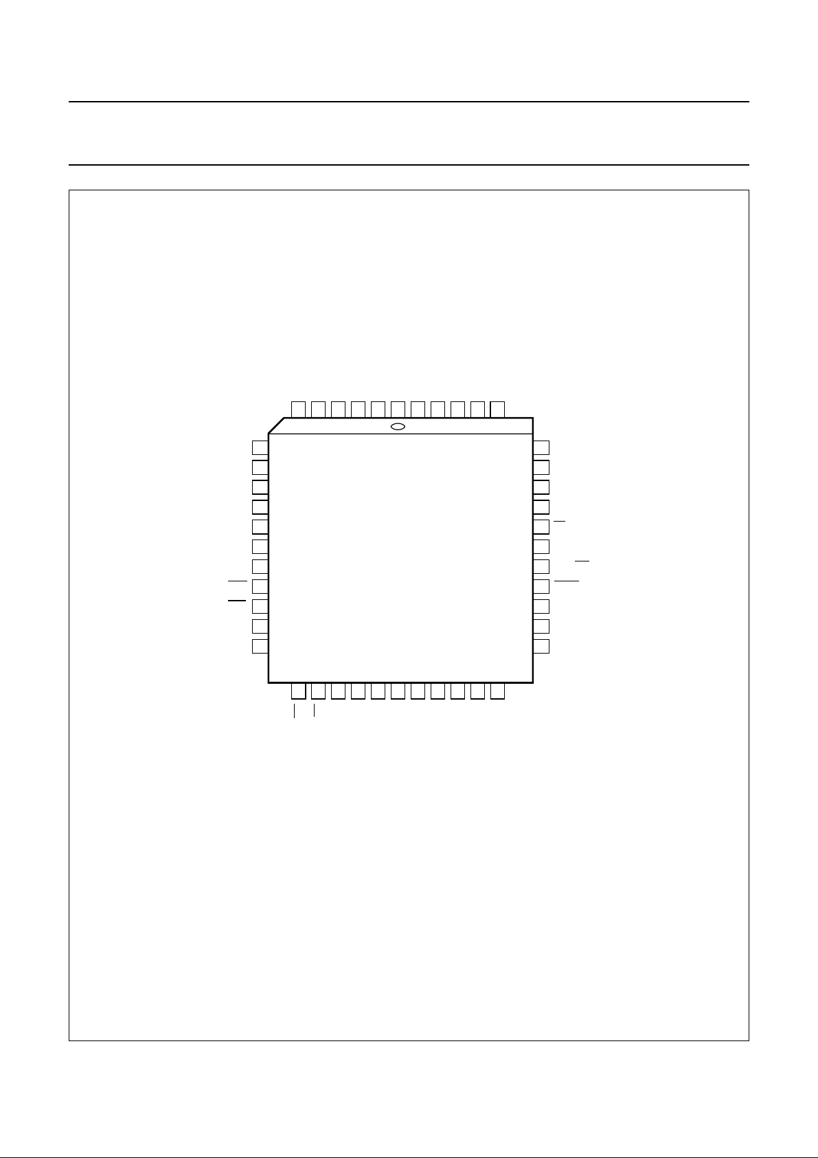
Fig.5 Pin configuration for QFP44 package; for more information on the version see Chapter 3.
1997 Dec 15 8
Philips Semiconductors Product specification
8-bit microcontrollers P89C738; P89C739
handbook, full pagewidth
P0.4/AD4
P5.4
P5.3
P0.5/AD5
P0.6/AD6
9
8
7
6
5
n.c.
4
P0.7/AD7
EA/VPPALE/WE
n.c.
3
2
1
P2.7/AD15
P2.6/AD14
P5.2
P5.1
62
P2.5/AD13
61
PSEN
n.c.
68
67
66
65
64
63
P5.5
P0.3/AD3
P0.2/AD2
P5.6
P0.1/AD1
P0.0/AD0
P5.7
V
DD
n.c.
P1.0/T2
P4.0
P1.1/T2EX
P1.2
P1.3
P4.1
P1.4
P4.2
10
11
12
13
14
15
16
17
18
19
20
21
22
23
24
25
26
P89C739ABA
60
P5.0
59
P2.4/AD12
58
P2.3/AD11
57
P4.7
56
P2.2/AD10
55
P2.1/AD9
54
P2.0/AD8
53
P4.6
n.c.
52
V
51
50
P4.5
49
XTAL1
48
XTAL2
47
P3.7/RD
46
P4.4
45
P3.6/WR
44
P4.3
SS
27
28
29
30
31
32
33
34
n.c.
n.c.
n.c.
P1.5
P1.6
P1.7
RST
P3.0/RXD/data
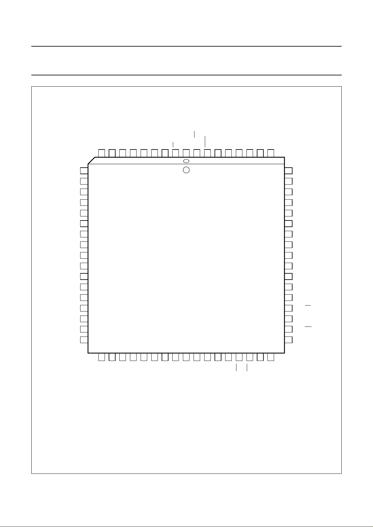
Fig.6 Pin configuration for PLCC68 package; for more information on the version see Chapter 3.
1997 Dec 15 9
35
n.c.
36
n.c.
37
n.c.
38
39
n.c.
P3.1/TXD/clock
40
41
P3.2/INT0
P3.3/INT1
42
P3.4/T0
43
MGK187
P3.5/T1
Philips Semiconductors Product specification
8-bit microcontrollers P89C738; P89C739
handbook, full pagewidth
PP
P5.4
64
P5.3
63
P0.5/AD5
P0.6/AD6
62
61
P0.7/AD7
60
EA/V
59
n.c.
58
ALE/WE
PSEN
57
56
P2.7/AD15
P2.6/AD14
55
54
P5.2
53
P5.1
52
P0.4/AD4
P5.5
P0.3/AD3
P0.2/AD2
P5.6
P0.1/AD1
P0.0/AD0
P5.7
V
DD
V
SS
P1.0/T2
P4.0
P1.1/T2EX
P1.2
P1.3
P4.1
P1.4
P4.2
P1.5
1
2
3
4
5
6
7
8
9
10
11
12
13
14
15
16
17
18
19
P89C739ABB
51
50
49
48
47
46
45
44
43
42
41
40
39
38
37
36
35
34
33
P2.5/AD13
P5.0
P2.4/AD12
P2.3/AD11
P4.7
P2.2/AD10
P2.1/AD9
P2.0/AD8
P4.6
n.c.
V
SS
P4.5
XTAL1
XTAL2
P3.7/RD
P4.4
P3.6/WR
P4.3
P3.5/T1
20
21
22
23
24
25
n.c.
n.c.
n.c.
P1.7
RST
P1.6
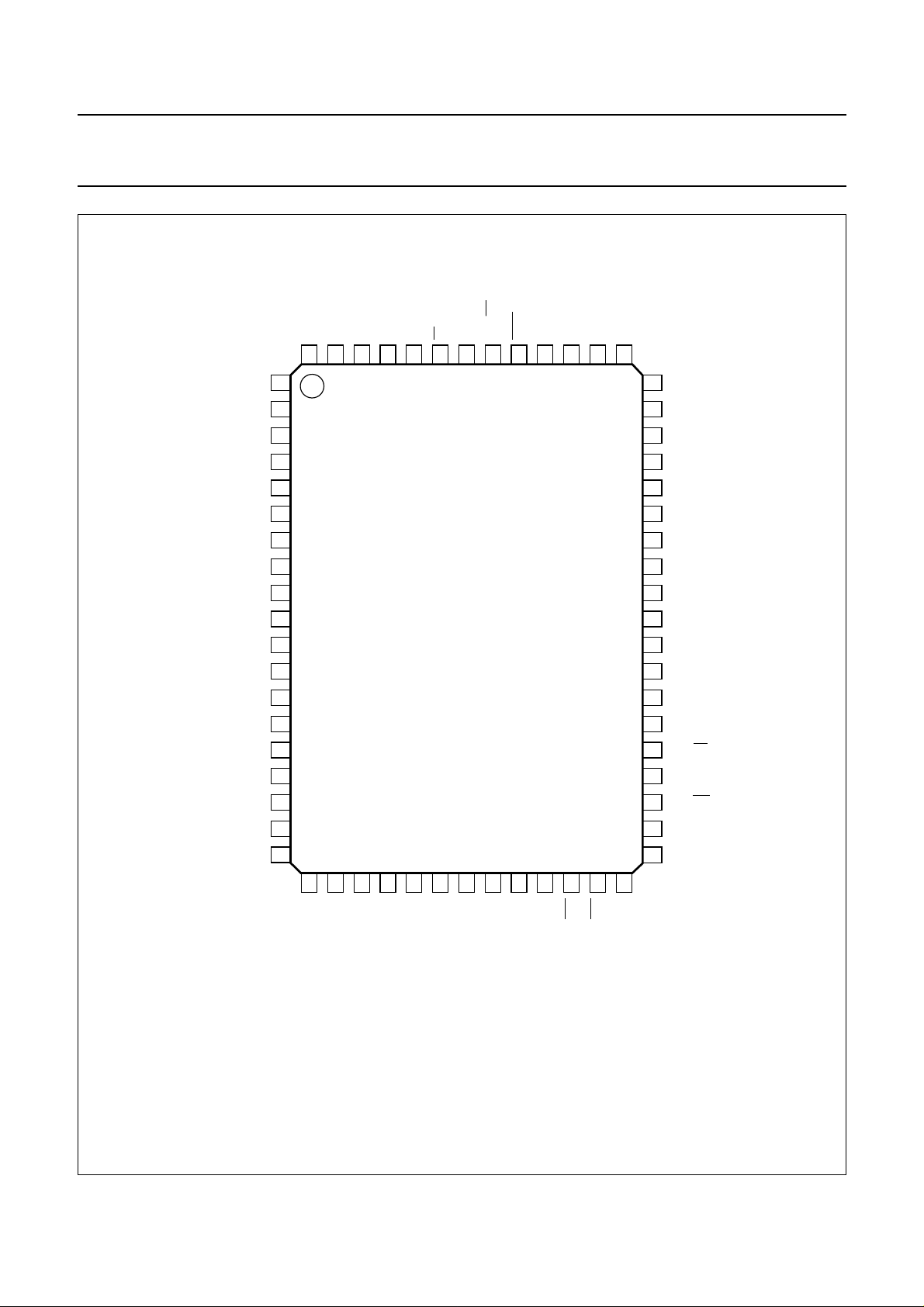
Fig.7 Pin configuration for QFP64 package (SOT319-1).
1997 Dec 15 10
26
27
28
n.c.
n.c.
P3.0/RXD/data
29
30
31
P3.2/INT0
P3.3/INT1
P3.1/TXD/clock
32
MGK188
P3.4/T0

1997 Dec 15 11
Table 1 Pin description for DIP40; QFP44; PLC44; QFP64 and PLCC68.
(1)
SYMBOL
PIN
DESCRIPTION
PLCC68 QFP64 PLCC44 QFP44 DIP40
P1.0/T2 19 11 16 2 1 Port 1: P1.0 to P1.7; 8-bit quasi-bidirectional I/O port. Port 1 can
P1.1/T2EX 21 13 15 3 2
P1.2 22 14 14 4 3
P1.3 23 15 13 5 4
P1.4 25 17 12 6 5
P1.5 27 19 1 7 6
sink/source one TTL (= 4 LSTTL) input. It can drive CMOS inputs
without external pull-ups.
Port 1 alternative functions are: T2; Timer/event counter 2 external
event counter input (falling edge triggered). T2EX; Timer/event
counter 2 capture/reload trigger or external interrupt 2 input (falling
edge triggered).
P1.6 28 20 2 8 7
P1.7 29 21 3 9 8
RST 30 22 4 10 9 Reset; a HIGH level on this pin for two machine cycles while the
oscillator is running, resets the device. An internal pull-down resistor
permits power-on reset using only a capacitor connected to V
After a Watchdog Timer overflow this pin is pulled HIGH while the
internal reset signal is active.
P3.0/RXD/data 34 26 5 11 10 Port 3: P3.0 to P3.7; 8-bit quasi-bidirectional I/O Port with internal
P3.1/TXD/clock 39 29 7 13 11
P3.2/
INT0 40 30 8 14 12
P3.3/
INT1 41 31 9 15 13
P3.4/T0 42 32 10 16 14
P3.5/T1 43 33 11 17 15
P3.6
WR 45 35 44 18 16
P3.7/
RD 47 37 43 19 17
pull-ups. Port 3 can sink/source one TTL (= 4 LSTTL) input. It can
drive CMOS inputs without external pull-ups.
Port 3 alternative functions are: RXD/data; Serial Port data input
(asynchronous) or data input/output (synchronous).
TXD/clock; Serial Port data output (asynchronous) or clock output
(synchronous). INT0; External interrupt 0 or gate control input for
Timer/event counter 0. INT1; External interrupt 1 or gate control
input for Timer/event counter 1. T0; external input for Timer/event
counter 0. T1; external input for Timer/event counter 1.
WR; external data memory write strobe. RD; external data memory
read strobe.
XTAL2 48 38 42 20 18 Crystal input 2: output of the inverting amplifier that forms the
oscillator. This pin left open-circuit when an external oscillator clock
is used (see Figs 18 and 20).
XTAL1 49 39 41 21 19 Crystal input 1: input to the inverting amplifier that forms the
oscillator, and input to the internal clock generator. Receives the
external oscillator clock signal when an external oscillator is used
(see Figs 18 and 20).
V
SS
51 41 40 22 20 Ground: circuit ground potential.
DD
6.2 Pin description
.
Philips Semiconductors Product specification
8-bit microcontrollers P89C738; P89C739

1997 Dec 15 12
(1)
SYMBOL
PIN
DESCRIPTION
PLCC68 QFP64 PLCC44 QFP44 DIP40
P2.0/A8 to
P2.2/A10
P2.3/A11 to
P2.4/A12
P2.5/A13 to
P2.7/A15
54 to 56 44 to 46 38 to 34 24 to 31 21 to 28 Port 2: P2.0 to P2.7; 8-bit quasi-bidirectional I/O Port with internal
pull-ups. Port 2 can sink/source one TTL (= 4 LSTTL) input. It can
58 to 59 48 to 49
drive CMOS inputs without external pull-ups.
Port 2 alternative functions are: A8 to A15; during access to
61, 64
and 65
51, 54
and 55
23 to 25
external memories (RAM/ROM) that use 16-bit addresses (MOVX
@DPTR) Port 2 emits the high-order address byte (A8 to A15).
PSEN 67 56 26 32 29 Program Store Enable output: read strobe to the external program
memory via Port 0 and Port 2. It is activated twice each machine
cycle during fetches from external program memory.
When executing out of external program memory two activations of
PSEN are skipped during each access to external data memory.
PSEN is not activated (remains HIGH) during no fetches from
external program memory .PSEN can sink/source 8 LSTTL inputs. It
can drive CMOS inputs without external pull-ups.
WE
(2)
68 57 27 33 30 Address Latch Enable output: latches the lower byte of the
ALE/
address during access to external memory in normal operation. It is
activated every six oscillator periods except during an external data
memory access. ALE can sink/source 8 LSTTL inputs. It can drive
CMOS inputs without an external pull-up.
WE: Write Enable.
EA/V
PP
2 59293531External Access input: when during reset, EA is held at a TTL
HIGH level, the CPU executes from the internal program ROM.
When EA is held at a TTL LOW level during reset, the CPU executes
out of external program memory via Port 0 and Port 2. EA is not
allowed to float. EA is latched during reset and don’t care after reset.
Philips Semiconductors Product specification
8-bit microcontrollers P89C738; P89C739
P0.7/AD7 to
P0.4/AD4
P0.3/AD3 to
P0.2/AD2
P0.1/AD1 to
P0.0/AD0
V
DD
VPP: programming supply voltage.
3, 5, 6
and 9
11 to 12 3 to 4 22 to 21
60, 61, 62
and 1
30 to 33 36 to 43 32 to 39 Port 0: P0.7 to P0.0; 8-bit open-drain bidirectional I/O port. It is also
the multiplexed low-order address and data bus during accesses to
external memory: AD0 to AD7. During these accesses internal
pull-ups are activated. Port 0 can sink/source 8 LSTTL inputs.
14 to 15 6 to 7 20 to 19
17 9 18 44 40 Power supply (+5 V) pin for normal operation, Idle mode and
Power-down mode.

1997 Dec 15 13
(1)
SYMBOL
PIN
DESCRIPTION
PLCC68 QFP64 PLCC44 QFP44 DIP40
P4.0 to P4.7 20, 24,
26, 44,
46, 50, 53
and 57
P5.0 to P5.7 60, 62,
63, 7, 8,
10, 13
and 16
n.c. 1, 4, 18,
31, 32,
33, 35,
36, 37, 38
12, 16,
18, 34,
36, 40, 43
and 47
50, 52,
53, 63,
64, 2, 5
and 8
23, 24,
25, 27,
28, 42
and 58
(3)
n.a.
n.a. n.a. Port 4: P4.0 to P4.7; 8-bit quai-bidirectional I/O port with internal
pull-ups. Port 4 can sink/source 4 LSTTL inputs. It can drive CMOS
inputs without external pull-ups.
n.a. n.a. n.a. Port 5: P5.0 to P5.7; 8-bit quai-bidirectional I/O port with internal
pull-ups. Port 5 can sink/source 4 LSTTL inputs. It can drive CMOS
inputs without external pull-ups.
6, 17, 28
and 39
1, 12, 23
and 34
n.a. Not connected.
52 and 66
Notes
1. To avoid a ‘latch-up’ effect at power-on, the voltage on any pin (at any time) must not be higher than VDD+ 0.5 V or lower than VSS− 0.5 V
respectively.
2. To prohibit the toggling of the ALE/WE pin (RFI noise reduction) the bit RFI in the PCON register (PCON.5) must be set by software. This bit is
cleared on reset and can be cleared by software. When set, ALE/WE pin will be pulled down internally, switching an external address latch to a
quiet state. The MOVX instruction will still toggle ALE/WE as a normal MOVX. ALE/WE will retain its normal HIGH value during Idle mode and a
LOW value during Power-down mode while in the ‘RFI’ mode. Additionally during internal access (EA = 1) ALE/WE will toggle normally when the
address exceeds the internal program memory size. During external access (EA = 0) ALE/WE will always toggle normally, whether the flag ‘RFI’ is
set or not.
3. n.a. = not applicable.
Philips Semiconductors Product specification
8-bit microcontrollers P89C738; P89C739

Philips Semiconductors Product specification
8-bit microcontrollers P89C738; P89C739
7 FUNCTIONAL DESCRIPTION
This chapter gives a brief overview of the device.
Detailed functional descriptions are given in the following
chapters:
Chapter 8 “Memory organization”
Chapter 9 “Interrupt system”
Chapter 10 “Timers/counters”
Chapter 11 “I/O facilities”
Chapter 12 “Full duplex Serial Port (UART)”
Chapter 13 “Reduced power modes”
Chapter 14 “Oscillator circuit”
Chapter 15 “Reset”
Chapter 16 “Multiple Programming ROM (MTP-ROM)”
7.1 General
The P89C738 is a stand-alone high-performance
microcontroller designed for use in real time applications
such as instrumentation, industrial control and medium to
high-end consumer applications.
In addition to the 80C51 standard functions, the device
provides a number of dedicated hardware functions for
these applications. The P89C738 is a control-oriented
CPU with on-chip Program and data memory. It can
execute programs with internal or external program
memory up to 64 kbytes. It can also access up to
64 kbytes of external data memory. For systems requiring
extra capability, the P89C738 can be expanded using
standard memories and peripherals.
The P89C738 has two software selectable modes of
reduced activity for further power reduction: Idle and
Power-down. The Idle mode freezes the CPU while
allowing the RAM, timers, serial ports and interrupt system
to continue functioning. The Power-down mode saves the
RAM contents but freezes the oscillator causing all other
chip functions to be inoperative except the Watchdog
Timer if it is enabled. The Power-down mode can be
terminated by an external reset, a Watchdog Timer
overflow and in addition, by either of the two external
interrupts.
7.2 Instruction set execution
The P89C738 uses the powerful instruction set of the
80C51. Additional Special Function Registers (SFRs) are
incorporated to control the on-chip peripherals.
The instruction set consists of 49 single-byte, 46 two-byte
and 16 three-byte instructions. When using a 16 MHz
oscillator, 64 instructions execute in 750 ns and
45 instructions execute in 1.5 µs. Multiply and divide
instructions execute in 3 µs (see Chapter 18).
1997 Dec 15 14

Philips Semiconductors Product specification
8-bit microcontrollers P89C738; P89C739
8 MEMORY ORGANIZATION
The Central Processing Unit (CPU) manipulates operands
in three memory spaces; these are the 64 kbyte external
data memory (of which the lower 256 bytes reside in the
internal AUX-RAM), 512 bytes internal data memory
(consisting of 256 bytes standard RAM and 256 bytes
AUX-RAM) and the 64 kbytes internal and external
program memory.
8.1 Program memory
The program memory address space of the P89C738
comprises an internal and an external memory portion.
The P89C738 has 64 kbytes of program memory on-chip.
The program memory can also be externally addressed up
to 64 kbytes. If the
EA pin is held HIGH, the P89C738
executes out of the internal program memory. If EA pin is
held LOW, the P89C738 fetches all instructions from the
external program memory. Figure 8 illustrates the program
memory address space.
The security bit is always set in the P89C738 and
P89C739 to protect the ROM code. Table 2 lists the
access to the internal and external program memory by the
MOVC instructions when the security bit has been set to a
logic 1. If the security bit has been set to a logic 0 there are
no restrictions for the MOVC instructions.
Table 2 Internal and external program memory access
MOVC
INSTRUCTION
MOVC in internal
PROGRAM MEMORY ACCESS
INTERNAL EXTERNAL
YES YES
program memory
MOVC in external
NO YES
program memory
8.2 Internal data memory
The internal data memory is divided into three physically
separated parts: 256 bytes of RAM, 256 bytes of
AUX-RAM, and a 128 bytes Special Function Registers
(SFRs) area. These parts can be addressed as follows
(see Fig.9 and Table 3):
• RAM locations 0 to 127 can be addressed directly and
indirectly as in the 80C51. Address pointers are R0 and
R1 of the selected register bank.
• RAM locations 128 to 255 can only be addressed
indirectly. Address pointers are R0 and R1 of the
selected register bank.
• AUX-RAM locations 0 to 255 are indirectly addressable
as the external data memory locations 0 to 255 with the
MOVX instructions. Address pointers are R0 and R1 of
the selected register bank and DPTR. When executing
from internal program memory, an access to AUX-RAM
0 to 255 will not affect the ports Port 0, Port 2,
P3.6 and P3.7.
• The SFRs can only be addressed directly in the address
range from 128 to 255.
An access to external data memory locations higher than
255 will be performed with the MOVX DPTR instructions in
the same way as in the 80C51 structure, i.e. with Port 0
and Port 2 as data/address bus and P3.6 and P3.7 as write
and read timing signals. Note that the external data
memory cannot be accessed with R0 and R1 as address
pointer.
Figure 9 shows the internal and external data memory
address space. Chapter 17 shows the Special Function
Registers overview. Four 8-bit register banks occupy
locations 0 through 31 in the lower RAM area. Only one of
these banks may be enabled at a time. The next 16 bytes,
locations 32 through 47, contain 128 directly addressable
bit locations.
handbook, halfpage
65535
0
INTERNAL
(EA = 1)
PROGRAM MEMORY
EXTERNAL
(EA = 0)
MGK190
Fig.8 Program memory address space.
1997 Dec 15 15
The stack can be located anywhere in the internal 256 byte
RAM. The stack depth is only limited by the available
internal RAM space of 256 bytes. All registers except the
Program Counter and the four 8-bit register banks reside
in the SFR address space.
Table 3 Internal data memory access
MEMORY LOCATION ADDRESS MODE
RAM 0 to 127 direct and indirect
128 to 255 indirect only
SFR 128 to 255 direct only
AUX-RAM 0 to 255 indirect only with MOVX

Philips Semiconductors Product specification
8-bit microcontrollers P89C738; P89C739
64K 64K
handbook, full pagewidth
INTERNAL
(EA = 1)
0
PROGRAM MEMORY
EXTERNAL
(EA = 0)
255
INDIRECT ONLY
127
DIRECT AND
INDIRECT
0
OVERLAPPED SPACE
MAIN RAM
INTERNAL DATA MEMORY
SFRs
AUXILIARY
RAM
MBK524
64K
256
EXTERNAL
DATA MEMORY
Fig.9 Internal and external data memory address space.
8.3 Addressing
The P89C738 has five modes for addressing:
• Register
• Direct
• Register-Indirect
• Immediate
• Base-Register plus Index-Register-Indirect.
The first three methods can be used for addressing
destination operands. Most instructions have a
‘destination/source’ field that specifies the data type,
addressing methods and operands involved. For
operations other than MOVs, the destination operand is
also a source operand.
Access to memory addresses is as follows:
• Register in one of the four 8-bit register banks through
Register, Direct or Register-Indirect addressing
• 512 bytes of internal RAM through Direct or
Register-Indirect addressing. Bytes 0 to 127 of internal
RAM may be addressed directly/indirectly. Bytes
128 to 255 of internal RAM share their address location
with the SFRs and so may only be addressed indirectly
as data RAM. Bytes 0 to 255 of AUX-RAM can only be
addressed indirectly via MOVX.
• SFR through Direct addressing at address locations
128 to 255
• External data memory through Register-Indirect
addressing
• Program memory look-up tables through Base-Register
plus Index-Register-Indirect addressing.
1997 Dec 15 16
Philips Semiconductors Product specification
8-bit microcontrollers P89C738; P89C739
9 INTERRUPT SYSTEM
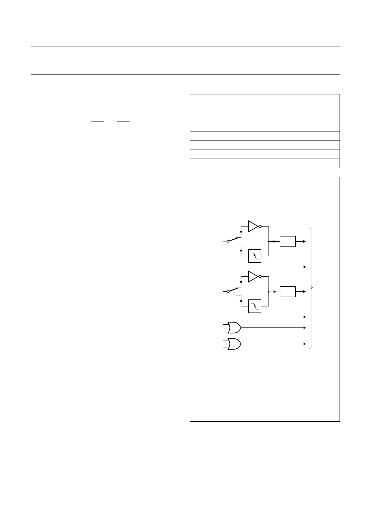
The P89C738 contains the same interrupt structure as the
PCB80C51BH, but with a six-source interrupt structure
with two priority levels (see Fig.10).
The external interrupts INT0 and INT1 can each be either
level-activated or transition-activated, depending on bits
IT0 and IT1 in SFR TCON. The flags that actually generate
these interrupts are bits IE0 and IE1 in TCON. When an
external interrupt is generated, the corresponding request
flag is cleared by the hardware when the service routine is
vectored to, only if the interrupt was transition-activated. If
the interrupt was level-activated the external source has to
hold the request active until the requested interrupt is
actually generated. Then it has to deactivate the request
before the interrupt service routine is completed, or else
another interrupt will be generated.
The Timer 0 and Timer 1 interrupts are generated by TF0
and TF1, which are set by a roll-over in their respective
timer/counter register (except for Timer 0 in Mode 3 of the
serial interface). When a timer interrupt is generated, the
flag that generated it is cleared by the on-chip hardware
when the service routine is vectored to.
The Serial Port interrupt is generated by the logical ‘OR’ of
RI and TI. Neither of these flags is cleared by hardware.
The service routine will normally have to determine
whether it was RI or TI that generated the interrupt, and the
bit will have to be cleared by software.
The Timer 2 interrupt is generated by the logical OR of TF2
and EXF2. Neither of these flags is cleared by hardware.
In fact the service routine may have to determine whether
it was TF2 or EXF2 that generated the interrupt, and the bit
will have to be cleared by software.
An additional (third) external interrupt is available, if
Timer 2 is not used as timer/counter or if Timer 2 is used
in the baud rate generator mode. That external interrupt 2
is falling-edge triggered. It shares the Timer 2 interrupt
vector, interrupt enable and interrupt priority bits. If bit
EXEN2 = 1 (T2CON.3), a HIGH-to-LOW transition at pin
P1.1/T2EX sets the interrupt request flag EXF2
(T2CON.6) and can be used to generate an external
interrupt.
The interrupt vectors are listed in Table 4.
Table 4 Interrupt vectors
SOURCE
PRIORITY
WITHIN LEVEL
VECTOR
ADDRESS
IE0 1 (highest) 0003H
TF0 2 000BH
IE1 3 0013H
TF1 4 001BH
RI + TI 5 0023H
TF2 + EXF2 6 (lowest) 002BH
handbook, halfpage
0
IT0INT0 IE0
1
TF0
0
IT1INT1
1
TF1
TI
RI
TF2
EXF2
IE1
MGK193
Fig.10 P89C738/P89C739 interrupt sources.
interrupt
sources
1997 Dec 15 17

Philips Semiconductors Product specification
8-bit microcontrollers P89C738; P89C739
9.1 Interrupt Enable Register (IE) Table 5 Interrupt Enable Register (SFR address A8H)
76543210
EA − ET2 ES ET1 EX1 ET0 EX0
Table 6 Description of IE bits
BIT SYMBOL DESCRIPTION
7EAGeneral enable/disable control. If EA = 0, no interrupt is enabled. If EA = 1, any
individually enabled interrupt will be accepted.
6 − reserved
5 ET2 enable Timer 2 interrupt
4 ES enable Serial Port interrupt
3 ET1 enable Timer 1 interrupt
2 EX1 enable external interrupt 1
1 ET0 enable Timer 0 interrupt
0 EX0 enable external interrupt 0
9.2 Interrupt Priority Register (IP) Table 7 Interrupt Priority Register (SFR address B8H)
76543210
−−PT2 PS PT1 PX1 PT0 PX0
Table 8 Description of IP bits
BIT SYMBOL DESCRIPTION
7 − reserved
6 − reserved
5 PT2 Timer 2 interrupt priority level
4 PS Serial Port interrupt priority level
3 PT1 Timer 1 interrupt priority level
2 PX1 external interrupt 1 priority level
1 PT0 Timer 0 interrupt priority level
0 PX0 external interrupt 0 priority level
1997 Dec 15 18

Philips Semiconductors Product specification
8-bit microcontrollers P89C738; P89C739
10 TIMERS/COUNTERS
The P89C738 contains three 16-bit timer/counters:
Timer 0, Timer 1 and Timer 2; and one 8-bit timer, the
Watchdog Timer (T3). Timer 0, Timer 1 and Timer 2 may
be programmed to carry out the following functions:
• Measure time intervals and pulse durations
• Count events
• Generate interrupt requests.
10.1 Timer 0 and Timer 1
Timers 0 and 1 each have a control bit in SFR TMOD that
selects the timer or counter function of the corresponding
timer. In the timer function, the register is incremented
every machine cycle. Thus, one can think of it as counting
machine cycles. Since a machine cycle consists
of 12 oscillator periods, the count rate is
1
⁄12 of the
oscillator frequency.
In the counter function, the register is incremented in
response to a HIGH-to-LOW transition at the
corresponding external input pin, T0 or T1. In this function,
the external input is sampled during S5P2 of every
machine cycle. When the samples show a HIGH in one
cycle and a LOW in the next cycle, the counter is
incremented. Thus, it takes two machine cycles
(24 oscillator periods) to recognize a HIGH-to-LOW
transition. There are no restrictions on the duty cycle of the
external input signal, but to ensure that a given level is
sampled at least once before it changes, it should be held
for at least one full machine cycle.
Timer 0 and Timer 1 can be programmed independently to
operate in one of four modes:
Mode 0 8-bit timer/counter with divide-by-32 prescaler
Mode 1 16-bit timer/counter
Mode 2 8-bit timer/counter with automatic reload
Mode 3 Timer 0: one 8-bit timer/counter and one 8-bit
timer. Timer 1: stopped.
When Timer 0 is in Mode 3, Timer 1 can be programmed
to operate in Modes 0, 1 or 2 but cannot set an interrupt
request flag and generate an interrupt. However, the
overflow from Timer 1 can be used to pulse the Serial Port
transmission-rate generator. With a 16 MHz crystal, the
counting frequency of these timer/counters is as follows:
• In the timer function, the timer is incremented at a
frequency of 1.33 MHz (
1
⁄12× oscillator frequency)
• In the counter function, the frequency handling range for
external inputs is 0 to 0.66 MHz.
Both internal and external inputs can be gated to the timer
by a second external source for directly measuring pulse
duration.
The timers are started and stopped under software control.
Each one sets its interrupt request flag when it overflows
from all logic 1's to all logic 0's (respectively, the automatic
reload value), with the exception of Mode 3 as previously
described.
10.1.1 Timer/Counter Mode Control Register (TMOD)
Table 9 Timer/Counter Mode Control Register (SFR address 89H)
76543210
GATE C/
TM1M0GATEC/TM1M0
Table 10 Description of TMOD bits for Timer 1 and Timer 0
Timer 0: bit TMOD.0 to TMOD.3; Timer 1: bit TMOD.4 to TMOD.7; n = 0, 1.
BIT SYMBOL DESCRIPTION
7 and 3 GATE Gating control. When set Timer/counter ‘n’ is enabled only when INTn pin is HIGH and
control bit TRn (TR1 or TR0) is set. When cleared Timer n is enabled whenever TRn
control bit is set.
6 and 2 C/
T Timer or Counter Selector. Cleared for Timer operation; input from internal system
clock. Set for Counter operation; input from pin Tn (T1 or T0).
5 and 1 M1 Timer 0, Timer 1 mode select; see Table 11.
4 and 0 M0
1997 Dec 15 19

Philips Semiconductors Product specification
8-bit microcontrollers P89C738; P89C739
Table 11 Timer 0; Timer 1 mode select
M1 M0 OPERATING
0 0 Timer TL0; TL1 serves as 5-bit prescaler.
0 1 16-bit Timer/Counter TH0; TH1 and TL0; TL1 are cascaded; there is no prescaler.
1 0 8-bit auto-reload Timer/Counter TH0; TH1 holds a value which is to be reloaded into
TL0; TL1 each time it overflows.
1 1 Timer 0: TL0 is an 8-bit Timer/Counter controlled by the standard Timer 0 control bits.
TH0 is an 8-bit timer only controlled by Timer 1 control bits.
1 1 Timer 1: Timer/Counter 1 stopped.
10.1.2 Timer/Counter Control Register (TCON)
Table 12 Timer/Counter Control Register (SFR address 88H)
76543210
TF1 TR1 TF0 TR0 IE1 IT1 IE0 IT0
Table 13 Description of TCON bits
BIT SYMBOL DESCRIPTION
7 and 5 TF1 and TF0 Timer 1 and Timer 0 overflow flags. Set by hardware on Timer/Counter overflow.
Cleared by hardware when processor vectors to interrupt routine.
6 and 4 TR1 and TR0 Timer 1 and Timer 0 run control bits. Set/cleared by software to turn Timer/Counter
on/off.
3 and 1 IE1 and IE0 Interrupt 1 and Interrupt 0 edge flags. Set by hardware when external interrupt edge
detected. Cleared when interrupt processed.
2 and 0 IT1 and IT0 Interrupt 1 and Interrupt 0 type control bits. Set/cleared by software to specify falling
edge/LOW level triggered external interrupts.
1997 Dec 15 20
 Loading...