

Philips P87LPC764BN Datasheet

INTEGRATED CIRCUITS
87LPC764
Low power, low price, low pin count
(20 pin) microcontroller with 4 kB OTP
Objective specification
Supersedes data of 1999 Dec 21
IC28 Data Handbook
2000 Apr 14

Philips Semiconductors Preliminary specification
Low power, low price, low pin count (20 pin)
microcontroller with 4 kB OTP
GENERAL DESCRIPTION 1. . . . . . . . . . . . . . . . . . . . . . . . . . . . . . . . . . . . . . . . . . . . . . . . . . . . . . . . . . . . . . . . . . . . . . . . . . . . . . . .
FEATURES 1. . . . . . . . . . . . . . . . . . . . . . . . . . . . . . . . . . . . . . . . . . . . . . . . . . . . . . . . . . . . . . . . . . . . . . . . . . . . . . . . . . . . . . . . . . . . .
ORDERING INFORMATION 1. . . . . . . . . . . . . . . . . . . . . . . . . . . . . . . . . . . . . . . . . . . . . . . . . . . . . . . . . . . . . . . . . . . . . . . . . . . . . . .
PIN CONFIGURATION, 20-PIN DIP AND SO PACKAGES 2. . . . . . . . . . . . . . . . . . . . . . . . . . . . . . . . . . . . . . . . . . . . . . . . . . . .
LOGIC SYMBOL 2. . . . . . . . . . . . . . . . . . . . . . . . . . . . . . . . . . . . . . . . . . . . . . . . . . . . . . . . . . . . . . . . . . . . . . . . . . . . . . . . . . . . . . . . .
BLOCK DIAGRAM 3. . . . . . . . . . . . . . . . . . . . . . . . . . . . . . . . . . . . . . . . . . . . . . . . . . . . . . . . . . . . . . . . . . . . . . . . . . . . . . . . . . . . . . .
PIN DESCRIPTIONS 5. . . . . . . . . . . . . . . . . . . . . . . . . . . . . . . . . . . . . . . . . . . . . . . . . . . . . . . . . . . . . . . . . . . . . . . . . . . . . . . . . . . . .
SPECIAL FUNCTION REGISTERS 6. . . . . . . . . . . . . . . . . . . . . . . . . . . . . . . . . . . . . . . . . . . . . . . . . . . . . . . . . . . . . . . . . . . . . . . . .
FUNCTIONAL DESCRIPTION 8. . . . . . . . . . . . . . . . . . . . . . . . . . . . . . . . . . . . . . . . . . . . . . . . . . . . . . . . . . . . . . . . . . . . . . . . . . . . .
Enhanced CPU 8. . . . . . . . . . . . . . . . . . . . . . . . . . . . . . . . . . . . . . . . . . . . . . . . . . . . . . . . . . . . . . . . . . . . . . . . . . . . . . . . . . . . . . . .
Analog Functions 8. . . . . . . . . . . . . . . . . . . . . . . . . . . . . . . . . . . . . . . . . . . . . . . . . . . . . . . . . . . . . . . . . . . . . . . . . . . . . . . . . . . . . .
Analog Comparators 8. . . . . . . . . . . . . . . . . . . . . . . . . . . . . . . . . . . . . . . . . . . . . . . . . . . . . . . . . . . . . . . . . . . . . . . . . . . . . . . . . . .
Comparator Configuration 8. . . . . . . . . . . . . . . . . . . . . . . . . . . . . . . . . . . . . . . . . . . . . . . . . . . . . . . . . . . . . . . . . . . . . . . . . . . .
Internal Reference Voltage 10. . . . . . . . . . . . . . . . . . . . . . . . . . . . . . . . . . . . . . . . . . . . . . . . . . . . . . . . . . . . . . . . . . . . . . . . . . .
Comparator Interrupt 10. . . . . . . . . . . . . . . . . . . . . . . . . . . . . . . . . . . . . . . . . . . . . . . . . . . . . . . . . . . . . . . . . . . . . . . . . . . . . . . .
Comparators and Power Reduction Modes 10. . . . . . . . . . . . . . . . . . . . . . . . . . . . . . . . . . . . . . . . . . . . . . . . . . . . . . . . . . . . .
Comparator Configuration Example 10. . . . . . . . . . . . . . . . . . . . . . . . . . . . . . . . . . . . . . . . . . . . . . . . . . . . . . . . . . . . . . . . . . . .
I2C Serial Interface 11. . . . . . . . . . . . . . . . . . . . . . . . . . . . . . . . . . . . . . . . . . . . . . . . . . . . . . . . . . . . . . . . . . . . . . . . . . . . . . . . . . . .
I2C Interrupts 11. . . . . . . . . . . . . . . . . . . . . . . . . . . . . . . . . . . . . . . . . . . . . . . . . . . . . . . . . . . . . . . . . . . . . . . . . . . . . . . . . . . . . . .
Reading I2CON 11. . . . . . . . . . . . . . . . . . . . . . . . . . . . . . . . . . . . . . . . . . . . . . . . . . . . . . . . . . . . . . . . . . . . . . . . . . . . . . . . . . . . .
Checking ATN and DRDY 13. . . . . . . . . . . . . . . . . . . . . . . . . . . . . . . . . . . . . . . . . . . . . . . . . . . . . . . . . . . . . . . . . . . . . . . . . . . .
Writing I2CON 13. . . . . . . . . . . . . . . . . . . . . . . . . . . . . . . . . . . . . . . . . . . . . . . . . . . . . . . . . . . . . . . . . . . . . . . . . . . . . . . . . . . . . .
Regarding Transmit Active 13. . . . . . . . . . . . . . . . . . . . . . . . . . . . . . . . . . . . . . . . . . . . . . . . . . . . . . . . . . . . . . . . . . . . . . . . . . .
Regarding Software Response Time 14. . . . . . . . . . . . . . . . . . . . . . . . . . . . . . . . . . . . . . . . . . . . . . . . . . . . . . . . . . . . . . . . . . .
Interrupts 15. . . . . . . . . . . . . . . . . . . . . . . . . . . . . . . . . . . . . . . . . . . . . . . . . . . . . . . . . . . . . . . . . . . . . . . . . . . . . . . . . . . . . . . . . . . . .
External Interrupt Inputs 16. . . . . . . . . . . . . . . . . . . . . . . . . . . . . . . . . . . . . . . . . . . . . . . . . . . . . . . . . . . . . . . . . . . . . . . . . . . . . .
I/O Ports 17. . . . . . . . . . . . . . . . . . . . . . . . . . . . . . . . . . . . . . . . . . . . . . . . . . . . . . . . . . . . . . . . . . . . . . . . . . . . . . . . . . . . . . . . . . . . . .
Quasi-Bidirectional Output Configuration 17. . . . . . . . . . . . . . . . . . . . . . . . . . . . . . . . . . . . . . . . . . . . . . . . . . . . . . . . . . . . . . .
Open Drain Output Configuration 18. . . . . . . . . . . . . . . . . . . . . . . . . . . . . . . . . . . . . . . . . . . . . . . . . . . . . . . . . . . . . . . . . . . . . .
Push-Pull Output Configuration 18. . . . . . . . . . . . . . . . . . . . . . . . . . . . . . . . . . . . . . . . . . . . . . . . . . . . . . . . . . . . . . . . . . . . . . .
Keyboard Interrupt (KBI) 19. . . . . . . . . . . . . . . . . . . . . . . . . . . . . . . . . . . . . . . . . . . . . . . . . . . . . . . . . . . . . . . . . . . . . . . . . . . . . . . .
Oscillator 21. . . . . . . . . . . . . . . . . . . . . . . . . . . . . . . . . . . . . . . . . . . . . . . . . . . . . . . . . . . . . . . . . . . . . . . . . . . . . . . . . . . . . . . . . . . . .
Low Frequency Oscillator Option 21. . . . . . . . . . . . . . . . . . . . . . . . . . . . . . . . . . . . . . . . . . . . . . . . . . . . . . . . . . . . . . . . . . . . . .
Medium Frequency Oscillator Option 21. . . . . . . . . . . . . . . . . . . . . . . . . . . . . . . . . . . . . . . . . . . . . . . . . . . . . . . . . . . . . . . . . . .
High Frequency Oscillator Option 21. . . . . . . . . . . . . . . . . . . . . . . . . . . . . . . . . . . . . . . . . . . . . . . . . . . . . . . . . . . . . . . . . . . . . .
On-Chip RC Oscillator Option 21. . . . . . . . . . . . . . . . . . . . . . . . . . . . . . . . . . . . . . . . . . . . . . . . . . . . . . . . . . . . . . . . . . . . . . . . .
External Clock Input Option 21. . . . . . . . . . . . . . . . . . . . . . . . . . . . . . . . . . . . . . . . . . . . . . . . . . . . . . . . . . . . . . . . . . . . . . . . . . .
Clock Output 21. . . . . . . . . . . . . . . . . . . . . . . . . . . . . . . . . . . . . . . . . . . . . . . . . . . . . . . . . . . . . . . . . . . . . . . . . . . . . . . . . . . . . . .
CPU Clock Modification: CLKR and DIVM 23. . . . . . . . . . . . . . . . . . . . . . . . . . . . . . . . . . . . . . . . . . . . . . . . . . . . . . . . . . . . . .
Power Monitoring Functions 23. . . . . . . . . . . . . . . . . . . . . . . . . . . . . . . . . . . . . . . . . . . . . . . . . . . . . . . . . . . . . . . . . . . . . . . . . . . . .
Brownout Detection 23. . . . . . . . . . . . . . . . . . . . . . . . . . . . . . . . . . . . . . . . . . . . . . . . . . . . . . . . . . . . . . . . . . . . . . . . . . . . . . . . .
Power On Detection 24. . . . . . . . . . . . . . . . . . . . . . . . . . . . . . . . . . . . . . . . . . . . . . . . . . . . . . . . . . . . . . . . . . . . . . . . . . . . . . . . .
Power Reduction Modes 24. . . . . . . . . . . . . . . . . . . . . . . . . . . . . . . . . . . . . . . . . . . . . . . . . . . . . . . . . . . . . . . . . . . . . . . . . . . . . . . .
Idle Mode 24. . . . . . . . . . . . . . . . . . . . . . . . . . . . . . . . . . . . . . . . . . . . . . . . . . . . . . . . . . . . . . . . . . . . . . . . . . . . . . . . . . . . . . . . . .
Power Down Mode 24. . . . . . . . . . . . . . . . . . . . . . . . . . . . . . . . . . . . . . . . . . . . . . . . . . . . . . . . . . . . . . . . . . . . . . . . . . . . . . . . . .
Low Voltage EPROM Operation 26. . . . . . . . . . . . . . . . . . . . . . . . . . . . . . . . . . . . . . . . . . . . . . . . . . . . . . . . . . . . . . . . . . . . . . .
Reset 26. . . . . . . . . . . . . . . . . . . . . . . . . . . . . . . . . . . . . . . . . . . . . . . . . . . . . . . . . . . . . . . . . . . . . . . . . . . . . . . . . . . . . . . . . . . . . . . .
Timer/Counters 27. . . . . . . . . . . . . . . . . . . . . . . . . . . . . . . . . . . . . . . . . . . . . . . . . . . . . . . . . . . . . . . . . . . . . . . . . . . . . . . . . . . . . . . .
Mode 0 28. . . . . . . . . . . . . . . . . . . . . . . . . . . . . . . . . . . . . . . . . . . . . . . . . . . . . . . . . . . . . . . . . . . . . . . . . . . . . . . . . . . . . . . . . . . .
Mode 1 29. . . . . . . . . . . . . . . . . . . . . . . . . . . . . . . . . . . . . . . . . . . . . . . . . . . . . . . . . . . . . . . . . . . . . . . . . . . . . . . . . . . . . . . . . . . .
Mode 2 29. . . . . . . . . . . . . . . . . . . . . . . . . . . . . . . . . . . . . . . . . . . . . . . . . . . . . . . . . . . . . . . . . . . . . . . . . . . . . . . . . . . . . . . . . . . .
Mode 3 29. . . . . . . . . . . . . . . . . . . . . . . . . . . . . . . . . . . . . . . . . . . . . . . . . . . . . . . . . . . . . . . . . . . . . . . . . . . . . . . . . . . . . . . . . . . .
Timer Overflow Toggle Output 30. . . . . . . . . . . . . . . . . . . . . . . . . . . . . . . . . . . . . . . . . . . . . . . . . . . . . . . . . . . . . . . . . . . . . . . .
UART 30. . . . . . . . . . . . . . . . . . . . . . . . . . . . . . . . . . . . . . . . . . . . . . . . . . . . . . . . . . . . . . . . . . . . . . . . . . . . . . . . . . . . . . . . . . . . . . . .
87LPC764
2000 Apr 15
i

Philips Semiconductors Preliminary specification
Low power, low price, low pin count (20 pin)
microcontroller with 4 kB OTP
Mode 0 30. . . . . . . . . . . . . . . . . . . . . . . . . . . . . . . . . . . . . . . . . . . . . . . . . . . . . . . . . . . . . . . . . . . . . . . . . . . . . . . . . . . . . . . . . . . .
Mode 1 30. . . . . . . . . . . . . . . . . . . . . . . . . . . . . . . . . . . . . . . . . . . . . . . . . . . . . . . . . . . . . . . . . . . . . . . . . . . . . . . . . . . . . . . . . . . .
Mode 2 30. . . . . . . . . . . . . . . . . . . . . . . . . . . . . . . . . . . . . . . . . . . . . . . . . . . . . . . . . . . . . . . . . . . . . . . . . . . . . . . . . . . . . . . . . . . .
Mode 3 30. . . . . . . . . . . . . . . . . . . . . . . . . . . . . . . . . . . . . . . . . . . . . . . . . . . . . . . . . . . . . . . . . . . . . . . . . . . . . . . . . . . . . . . . . . . .
Serial Port Control Register (SCON) 31. . . . . . . . . . . . . . . . . . . . . . . . . . . . . . . . . . . . . . . . . . . . . . . . . . . . . . . . . . . . . . . . . . .
Baud Rates 32. . . . . . . . . . . . . . . . . . . . . . . . . . . . . . . . . . . . . . . . . . . . . . . . . . . . . . . . . . . . . . . . . . . . . . . . . . . . . . . . . . . . . . . .
Using Timer 1 to Generate Baud Rates 32. . . . . . . . . . . . . . . . . . . . . . . . . . . . . . . . . . . . . . . . . . . . . . . . . . . . . . . . . . . . . . . . .
More About UART Mode 0 34. . . . . . . . . . . . . . . . . . . . . . . . . . . . . . . . . . . . . . . . . . . . . . . . . . . . . . . . . . . . . . . . . . . . . . . . . . .
More About UART Mode 1 34. . . . . . . . . . . . . . . . . . . . . . . . . . . . . . . . . . . . . . . . . . . . . . . . . . . . . . . . . . . . . . . . . . . . . . . . . . .
More About UART Modes 2 and 3 37. . . . . . . . . . . . . . . . . . . . . . . . . . . . . . . . . . . . . . . . . . . . . . . . . . . . . . . . . . . . . . . . . . . . .
Multiprocessor Communications 37. . . . . . . . . . . . . . . . . . . . . . . . . . . . . . . . . . . . . . . . . . . . . . . . . . . . . . . . . . . . . . . . . . . . . . .
Automatic Address Recognition 40. . . . . . . . . . . . . . . . . . . . . . . . . . . . . . . . . . . . . . . . . . . . . . . . . . . . . . . . . . . . . . . . . . . . . . .
Watchdog Timer 40. . . . . . . . . . . . . . . . . . . . . . . . . . . . . . . . . . . . . . . . . . . . . . . . . . . . . . . . . . . . . . . . . . . . . . . . . . . . . . . . . . . . . . .
Watchdog Feed Sequence 40. . . . . . . . . . . . . . . . . . . . . . . . . . . . . . . . . . . . . . . . . . . . . . . . . . . . . . . . . . . . . . . . . . . . . . . . . . .
Watchdog Reset 40. . . . . . . . . . . . . . . . . . . . . . . . . . . . . . . . . . . . . . . . . . . . . . . . . . . . . . . . . . . . . . . . . . . . . . . . . . . . . . . . . . . .
Additional Features 42. . . . . . . . . . . . . . . . . . . . . . . . . . . . . . . . . . . . . . . . . . . . . . . . . . . . . . . . . . . . . . . . . . . . . . . . . . . . . . . . . . . .
Software Reset 42. . . . . . . . . . . . . . . . . . . . . . . . . . . . . . . . . . . . . . . . . . . . . . . . . . . . . . . . . . . . . . . . . . . . . . . . . . . . . . . . . . . . .
Dual Data Pointers 42. . . . . . . . . . . . . . . . . . . . . . . . . . . . . . . . . . . . . . . . . . . . . . . . . . . . . . . . . . . . . . . . . . . . . . . . . . . . . . . . . .
EPROM Characteristics 43. . . . . . . . . . . . . . . . . . . . . . . . . . . . . . . . . . . . . . . . . . . . . . . . . . . . . . . . . . . . . . . . . . . . . . . . . . . . . . . .
32-Byte Customer Code Space 43. . . . . . . . . . . . . . . . . . . . . . . . . . . . . . . . . . . . . . . . . . . . . . . . . . . . . . . . . . . . . . . . . . . . . . .
System Configuration Bytes 43. . . . . . . . . . . . . . . . . . . . . . . . . . . . . . . . . . . . . . . . . . . . . . . . . . . . . . . . . . . . . . . . . . . . . . . . . .
Security Bits 44. . . . . . . . . . . . . . . . . . . . . . . . . . . . . . . . . . . . . . . . . . . . . . . . . . . . . . . . . . . . . . . . . . . . . . . . . . . . . . . . . . . . . . . .
ABSOLUTE MAXIMUM RATINGS 44. . . . . . . . . . . . . . . . . . . . . . . . . . . . . . . . . . . . . . . . . . . . . . . . . . . . . . . . . . . . . . . . . . . . . . . . .
DC ELECTRICAL CHARACTERISTICS 45. . . . . . . . . . . . . . . . . . . . . . . . . . . . . . . . . . . . . . . . . . . . . . . . . . . . . . . . . . . . . . . . . . . .
COMPARATOR ELECTRICAL CHARACTERISTICS 46. . . . . . . . . . . . . . . . . . . . . . . . . . . . . . . . . . . . . . . . . . . . . . . . . . . . . . . . .
AC ELECTRICAL CHARACTERISTICS 46. . . . . . . . . . . . . . . . . . . . . . . . . . . . . . . . . . . . . . . . . . . . . . . . . . . . . . . . . . . . . . . . . . . .
87LPC764
2000 Apr 15
ii
Philips Semiconductors Objective specification
Low power, low price, low pin count (20 pin)
microcontroller with 4 kB OTP
GENERAL DESCRIPTION
The 87LPC764 is a 20-pin single-chip microcontroller designed for
low pin count applications demanding high-integration, low cost
solutions over a wide range of performance requirements. A
member of the Philips low pin count family, the 87LPC764 of fers
programmable oscillator configurations for high and low speed
crystals or RC operation, wide operating voltage range,
programmable port output configurations, selectable Schmitt trigger
inputs, LED drive outputs, and a built-in watchdog timer. The
87LPC764 is based on an accelerated 80C51 processor
architecture that executes instructions at twice the rate of standard
80C51 devices.
FEA TURES
•An accelerated 80C51 CPU provides instruction cycle times of
300–600 ns for all instructions except multiply and divide when
executing at 20 MHz. Execution at up to 20 MHz when
V
= 4.5 V to 6.0 V, 10 MHz when VDD = 2.7 V to 6.0 V.
DD
•2.7 V to 6.0 V operating range for digital functions.
•4 K bytes EPROM code memory.
•128 byte RAM data memory.
•32-byte customer code EPROM allows serialization of devices,
storage of setup parameters, etc.
•Two 16-bit counter/timers. Each timer may be configured to toggle
a port output upon timer overflow.
•Two analog comparators.
•Full duplex UART.
2
•I
C communication port.
•Eight keypad interrupt inputs, plus two additional external interrupt
inputs.
•Four interrupt priority levels.
•Watchdog timer with separate on-chip oscillator , requiring no
external components. The watchdog timeout time is selectable
from 8 values.
•Active low reset. On-chip power-on reset allows operation with no
external reset components.
•Low voltage reset. One of two preset low voltage levels may be
selected to allow a graceful system shutdown when power fails.
May optionally be configured as an interrupt.
•Oscillator Fail Detect. The watchdog timer has a separate fully
on-chip oscillator, allowing it to perform an oscillator fail detect
function.
•Configurable on-chip oscillator with frequency range and RC
oscillator options (selected by user programmed EPROM bits).
The RC oscillator option allows operation with no external
oscillator components.
•Programmable port output configuration options:
quasi-bidirectional, open drain, push-pull, input-only.
•Selectable Schmitt trigger port inputs.
•LED drive capability (20 mA) on all port pins.
•Controlled slew rate port outputs to reduce EMI. Outputs have
approximately 10 ns minimum ramp times.
•15 I/O pins minimum. Up to 18 I/O pins using on-chip oscillator
and reset options.
•Only power and ground connections are required to operate the
87LPC764 when fully on-chip oscillator and reset options are
selected.
•Serial EPROM programming allows simple in-circuit production
coding. Two EPROM security bits prevent reading of sensitive
application programs.
•Idle and Power Down reduced power modes. Improved wakeup
from Power Down mode (a low interrupt input starts execution).
Typical Power Down current is 1 µA.
•20-pin DIP and SO packages.
87LPC764
ORDERING INFORMATION
Part Number Temperature Range °C and Package Frequency Drawing Number
P87LPC764B N 0 to +70, Plastic Dual In-Line Package 20 MHz (5 V), 10 MHz (3 V) SOT146–1
P87LPC764B D 0 to +70, Plastic Small Outline Package 20 MHz (5 V), 10 MHz (3 V) SOT163–1
P87LPC764F N –45 to +85, Plastic Dual In-Line Package 20 MHz (5 V), 10 MHz (3 V) SOT146–1
P87LPC764F D –45 to +85, Plastic Small Outline Package 20 MHz (5 V), 10 MHz (3 V) SOT163–1
2000 Apr 14
1
Philips Semiconductors Objective specification
Low power, low price, low pin count (20 pin)
microcontroller with 4 kB OTP
PIN CONFIGURATION, 20-PIN DIP AND SO PACKAGES
P1.7
P1.6
/P1.5
V
X1/P2.1
/P1.4
/P1.3
1
2
3
4
5
SS
6
7
8
9
10
CMP2/P0.0
RST
X2/CLKOUT/P2.0
INT1
SDA/INT0
SCL/T0/P1.2
LOGIC SYMBOL
P0.1/CIN2B
20
19
P0.2/CIN2A
18
P0.3/CIN1B
17
P0.4/CIN1A
16
P0.5/CMPREF
15
V
DD
14
P0.6/CMP1
13
P0.7/T1
12
P1.0/TxD
11
P1.1/RxD
87LPC764
SU01149
CIN2B
CIN2A
CIN1B
CIN1A
CMPREF
CMP1
CLKOUT/X2
V
V
DD
SS
TxDCMP2
RxD
T0 SCL
INT0
PORT 0PORT 2
T1
X1
PORT 1
INT1
RST
SDA
SU01150
2000 Apr 14
2
Philips Semiconductors Objective specification
Low power, low price, low pin count (20 pin)
microcontroller with 4 kB OTP
BLOCK DIAGRAM
ACCELERATED
80C51 CPU
INTERNAL BUS
4K BYTE
CODE EPROM
128 BYTE
DATA RAM
PORT 2
CONFIGURABLE I/OS
87LPC764
UART
I2C
TIMER 0, 1
CRYSTAL OR
RESONATOR
PORT 1
CONFIGURABLE I/OS
PORT 0
CONFIGURABLE I/OS
KEYPAD
INTERRUPT
CONFIGURABLE
OSCILLATOR
ON-CHIP
R/C
OSCILLATOR
WATCHDOG TIMER
AND OSCILLATOR
ANALOG
COMPARATORS
POWER MONITOR
(POWER-ON RESET,
BROWNOUT RESET)
SU01151
2000 Apr 14
3
Philips Semiconductors Objective specification
Low power, low price, low pin count (20 pin)
microcontroller with 4 kB OTP
FFFFh
UNUSED CODE
MEMORY SPACE
32-BYTE CUSTOMER
CODE SPACE
(ACCESSIBLE VIA MOVC)
UNUSED CODE
MEMORY SPACE
4 K BYTES ON-CHIP
CODE MEMORY
INTERRUPT VECTORS
ON-CHIP CODE
MEMORY SPACE
FCFFh
FCE0h
1000h
0FFFh
0000h
SPECIAL FUNCTION
REGISTERS
(ONLY DIRECTLY
ADDRESSABLE)
128 BYTES ON-CHIP DATA
MEMORY
(DIRECTLY AND
INDIRECTLY
ADDRESSABLE)
16-BIT ADDRESSABLE BYTES
ON-CHIP DATA
MEMORY SPACE
87LPC764
FFFFh
UNUSED SPACE
CONFIGURATION BYTES
UCFG1, UCFG2
(ACCESSIBLE VIA MOVX)
FFh
80h
7Fh
00h 0000h
UNUSED SPACE
EXTERNAL DATA
MEMORY SPACE*
FD01h
FD00h
* The 87LPC764 does not support access to external data memory. However, the User Configuration Bytes
are accessed via the MOVX instruction as if they were in external data memory.
Figure 1. 87LPC764 Program and Data Memory Map
SU01216
2000 Apr 14
4

Philips Semiconductors Objective specification
Low power, low price, low pin count (20 pin)
87LPC764
microcontroller with 4 kB OTP
PIN DESCRIPTIONS
MNEMONIC PIN NO. TYPE NAME AND FUNCTION
P0.0–P0.7 1, 13, 14,
P1.0–P1.7 2–4, 8–12 I/O Port 1: Port 1 is an 8-bit I/O port with a user-configurable output type, except for three pins as noted
P2.0–P2.1 6, 7 I/O Port 2: Port 2 is a 2-bit I/O port with a user-configurable output type. Port 2 latches are configured in the
V
SS
V
DD
16–20
1 O P0.0 CMP2 Comparator 2 output.
20 I P0.1 CIN2B Comparator 2 positive input B.
19 I P0.2 CIN2A Comparator 2 positive input A.
18 I P0.3 CIN1B Comparator 1 positive input B.
17 I P0.4 CIN1A Comparator 1 positive input A.
16 I P0.5 CMPREF Comparator reference (negative) input.
14 O P0.6 CMP1 Comparator 1 output.
13 I/O P0.7 T1 Timer/counter 1 external count input or overflow output.
12 O P1.0 TxD Transmitter output for the serial port.
11 I P1.1 RxD Receiver input for the serial port.
10 I/O
9 I
8 I P1.4 INT1 External interrupt 1 input.
4 I P1.5 RST External Reset input (if selected via EPROM configuration). A low on this pin
7 O P2.0 X2 Output from the oscillator amplifier (when a crystal oscillator option is
6 I P2.1 X1 Input to the oscillator circuit and internal clock generator circuits (when
5 I Ground: 0V reference.
15 I Power Supply: This is the power supply voltage for normal operation as well as Idle and
I/O Port 0: Port 0 is an 8-bit I/O port with a user-configurable output type. Port 0 latches are configured in
the quasi-bidirectional mode and have either ones or zeros written to them during reset, as determined
by the PRHI bit in the UCFG1 configuration byte. The operation of port 0 pins as inputs and outputs
depends upon the port configuration selected. Each port pin is configured independently. Refer to the
section on I/O port configuration and the DC Electrical Characteristics for details.
The Keyboard Interrupt feature operates with port 0 pins.
Port 0 also provides various special functions as described below.
below. Port 1 latches are configured in the quasi-bidirectional mode and have either ones or zeros
written to them during reset, as determined by the PRHI bit in the UCFG1 configuration byte. The
operation of the configurable port 1 pins as inputs and outputs depends upon the port configuration
selected. Each of the configurable port pins are programmed independently. Refer to the section on I/O
port configuration and the DC Electrical Characteristics for details.
Port 1 also provides various special functions as described below.
P1.2 T0 Timer/counter 0 external count input or overflow output.
I/O
P1.3 INT0 External interrupt 0 input.
I/O
quasi-bidirectional mode and have either ones or zeros written to them during reset, as determined by
the PRHI bit in the UCFG1 configuration byte. The operation of port 2 pins as inputs and outputs
depends upon the port configuration selected. Each port pin is configured independently. Refer to the
section on I/O port configuration and the DC Electrical Characteristics for details.
Port 2 also provides various special functions as described below.
Power Down modes.
SCL I2C serial clock input/output. When configured as an output, P1.2 is open
SDA I2C serial data input/output. When configured as an output, P1.3 is open
CLKOUT CPU clock divided by 6 clock output when enabled via SFR bit and in
drain, in order to conform to I
drain, in order to conform to I
resets the microcontroller, causing I/O ports and peripherals to take on their
default states, and the processor begins execution at address 0. When used
as a port pin, P1.5 is a Schmitt trigger input only.
selected via the EPROM configuration).
conjunction with internal RC oscillator or external clock input.
selected via the EPROM configuration).
2
C specifications.
2
C specifications.
2000 Apr 14
5
Philips Semiconductors Objective specification
Low power, low price, low pin count (20 pin)
87LPC764
microcontroller with 4 kB OTP
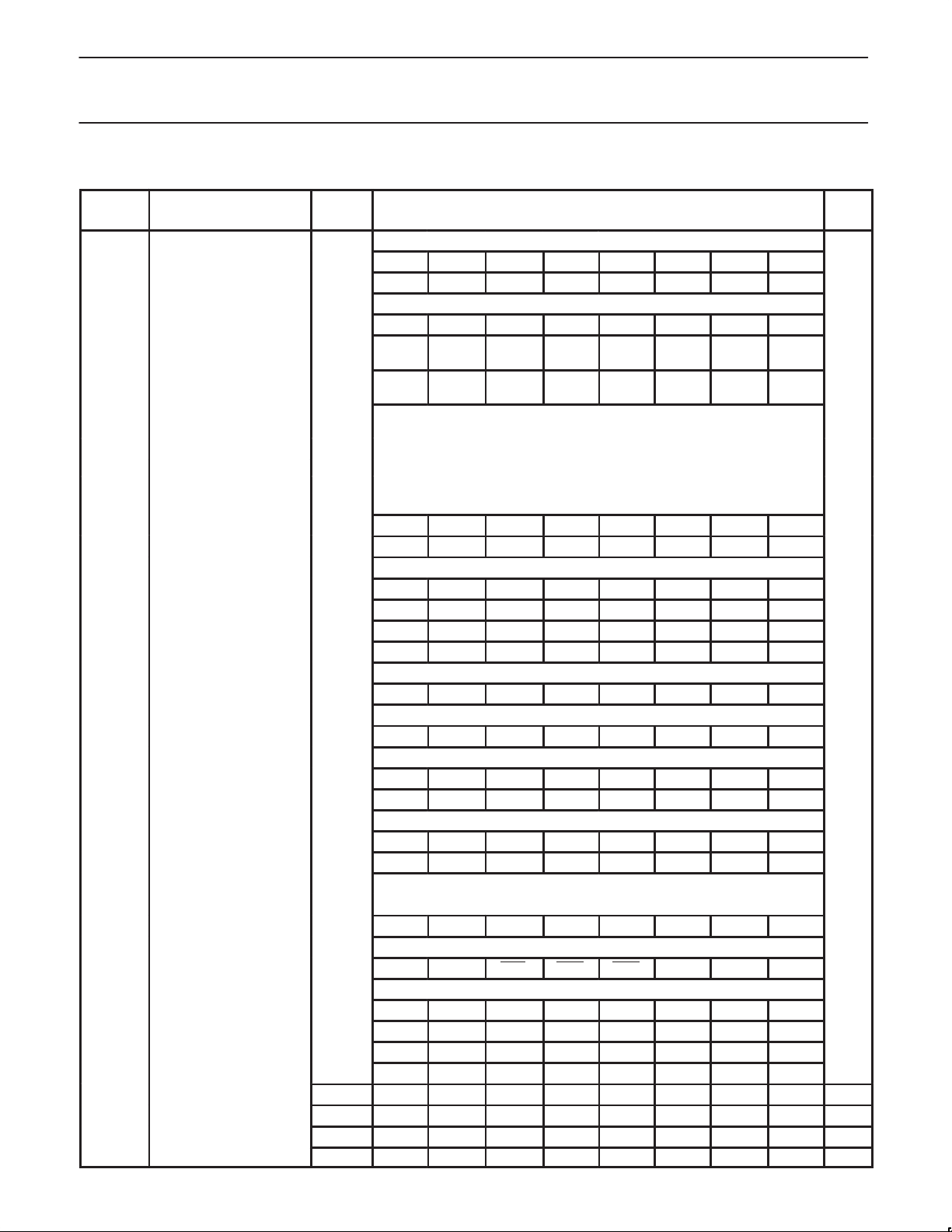
SPECIAL FUNCTION REGISTERS
Name Description
SFR
Address
MSB LSB
E7 E6 E5 E4 E3 E2 E1 E0
ACC* Accumulator E0h 00h
AUXR1# Auxiliary Function Register A2h KBF BOD BOI LPEP SRST 0 – DPS 02h
F7 F6 F5 F4 F3 F2 F1 F0
B* B register F0h 00h
CMP1#
CMP2#
DIVM#
Comparator 1 control
register
Comparator 2 control
register
CPU clock divide-by-M
control
ACh – – CE1 CP1 CN1 OE1 CO1 CMF1 00h
ADh – – CE2 CP2 CN2 OE2 CO2 CMF2 00h
95h 00h
DPTR: Data pointer (2 bytes)
DPH Data pointer high byte 83h 00h
DPL Data pointer low byte 82h 00h
CF CE CD CC CB CA C9 C8
I2CFG#* I2C configuration register C8h/RD SLAVEN MASTRQ 0 TIRUN – – CT1 CT0 00h
C8h/WR SLAVEN MASTRQ CLRTI TIRUN – – CT1 CT0
DF DE DD DC DB DA D9 D8
I2CON#* I2C control register D8h/RD RDA T ATN DRDY ARL STR STP
D8h/WR CXA IDLE CDR CARL CSTR CSTP XSTR XSTP
I2DAT# I2C data register D9h/RD RDA T 0 0 0 0 0 0 0 80h
D9h/WR XDAT x x x x x x x
AF AE AD AC AB AA A9 A8
IEN0* Interrupt enable 0 A8h EA EWD EBO ES ET1 EX1 ET0 EX0 00h
EF EE ED EC EB EA E9 E8
IEN1#* Interrupt enable 1 E8h ETI – EC1 – – EC2 EKB EI2 00h
BF BE BD BC BB BA B9 B8
IP0* Interrupt priority 0 B8h – PWD PBO PS PT1 PX1 PT0 PX0 00h
IP0H# Interrupt priority 0 high byte B7h – PWDH PBOH PSH PT1H PX1H PT0H PX0H 00h
FF FE FD FC FB FA F9 F8
IP1* Interrupt priority 1 F8h PTI – PC1 – – PC2 PKB PI2 00h
IP1H# Interrupt priority 1 high byte F7h PTIH – PC1H – – PC2H PKBH PI2H 00h
KBI# Keyboard Interrupt 86h 00h
87 86 85 84 83 82 81 80
P0* Port 0 80h T1 CMP1 CMPREF CIN1A CIN1B CIN2A CIN2B CMP2 Note 2
97 96 95 94 93 92 91 90
P1* Port 1 90h (P1.7) (P1.6) RST INT1 INT0 T0 RxD TxD Note 2
A7 A6 A5 A4 A3 A2 A1 A0
P2* Port 2 A0h – – – – – – X1 X2 Note 2
P0M1# Port 0 output mode 1 84h (P0M1.7) (P0M1.6) (P0M1.5) (P0M1.4) (P0M1.3) (P0M1.2) (P0M1.1) (P0M1.0) 00h
P0M2# Port 0 output mode 2 85h (P0M2.7) (P0M2.6) (P0M2.5) (P0M2.4) (P0M2.3) (P0M2.2) (P0M2.1) (P0M2.0) 00H
P1M1# Port 1 output mode 1 91h (P1M1.7) (P1M1.6) – (P1M1.4) – – (P1M1.1) (P1M1.0) 00h
P1M2# Port 1 output mode 2 92h (P1M2.7) (P1M2.6) – (P1M2.4) – – (P1M2.1) (P1M2.0) 00h
P2M1# Port 2 output mode 1 A4h P2S P1S P0S ENCLK T1OE T0OE (P2M1.1) (P2M1.0) 00h
P2M2# Port 2 output mode 2 A5h – – – – – – (P2M2.1) (P2M2.0) 00h
PCON Power control register 87h SMOD1 SMOD0 BOF POF GF1 GF0 PD IDL Note 3
Bit Functions and Addresses
MASTER
Reset
Value
– 80h
1
1
1
1
1
1
1
1
1
1
1
1
1
2000 Apr 14
6
Philips Semiconductors Objective specification
Low power, low price, low pin count (20 pin)
87LPC764
microcontroller with 4 kB OTP
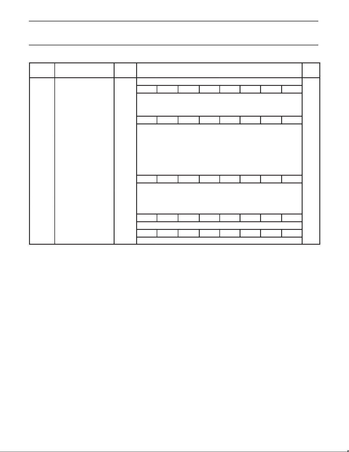
Name
PSW* Program status word D0h CY AC F0 RS1 RS0 OV F1 P 00h
PT0AD# Port 0 digital input disable F6h 00h
SCON* Serial port control 98h SM0 SM1 SM2 REN TB8 RB8 TI RI 00h
SBUF
SADDR# Serial port address register A9h 00h
SADEN# Serial port address enable B9h 00h
SP Stack pointer 81h 07h
TCON* Timer 0 and 1 control 88h TF1 TR1 TF0 TR0 IE1 IT1 IE0 IT0 00h
TH0 Timer 0 high byte 8Ch 00h
TH1 Timer 1 high byte 8Dh 00h
TL0 Timer 0 low byte 8Ah 00h
TL1 Timer 1 low byte 8Bh 00h
TMOD Timer 0 and 1 mode 89h GATE C/T M1 M0 GATE C/T M1 M0 00h
Description
Serial port data buffer
register
SFR
Address
99h xxh
MSB LSB
D7 D6 D5 D4 D3 D2 D1 D0
9F 9E 9D 9C 9B 9A 99 98
8F 8E 8D 8C 8B 8A 89 88
Bit Functions and Addresses
Reset
Value
WDCON# Watchdog control register A7h – –
WDRST# W atchdog reset register A6h xxh
NOTES:
* SFRs are bit addressable.
# SFRs are modified from or added to the 80C51 SFRs.
1. Unimplemented bits in SFRs are X (unknown) at all times. Ones should not be written to these bits since they may be used for other
purposes in future derivatives. The reset value shown in the table for these bits is 0.
2. I/O port values at reset are determined by the PRHI bit in the UCFG1 configuration byte.
3. The PCON reset value is x x BOF POF–0 0 0 0b. The BOF and POF flags are not affected by reset. The POF flag is set by hardware upon
power up. The BOF flag is set by the occurrence of a brownout reset/interrupt and upon power up.
4. The WDCON reset value is xx11 0000b for a Watchdog reset, xx01 0000b for all other reset causes if the watchdog is enabled, and xx00
0000b for all other reset causes if the watchdog is disabled.
WDOVF
WDRUN WDCLK WDS2 WDS1 WDS0 Note 4
2000 Apr 14
7

Philips Semiconductors Objective specification
Low power, low price, low pin count (20 pin)
microcontroller with 4 kB OTP
FUNCTIONAL DESCRIPTION
Details of 87LPC764 functions will be described in the following
sections.
Enhanced CPU
The 87LPC764 uses an enhanced 80C51 CPU which runs at twice the
speed of standard 80C51 devices. This means that the performance of
the 87LPC764 running at 5 MHz is exactly the same as that of a
standard 80C51 running at 10 MHz. A machine cycle consists of 6
oscillator cycles, and most instructions execute in 6 or 12 clocks. A
user configurable option allows restoring standard 80C51 execution
timing. In that case, a machine cycle becomes 12 oscillator cycles.
In the following sections, the term “CPU clock” is used to refer to the
clock that controls internal instruction execution. This may
sometimes be different from the externally applied clock, as in the
case where the part is configured for standard 80C51 timing by
means of the CLKR configuration bit or in the case where the clock
is divided down via the setting of the DIVM register. These features
are described in the Oscillator section.
Analog Functions
The 87LPC764 incorporates two Analog Comparators. In order to
give the best analog function performance and to minimize power
consumption, pins that are actually being used for analog functions
must have the digital outputs and the digital inputs disabled.
Digital outputs are disabled by putting the port output into the Input
Only (high impedance) mode as described in the I/O Ports section.
Digital inputs on port 0 may be disabled through the use of the
PT0AD register. Each bit in this register corresponds to one pin of
87LPC764
Port 0. Setting the corresponding bit in PT0AD disables that pin’s
digital input. Port bits that have their digital inputs disabled will be
read as 0 by any instruction that accesses the port.
Analog Comparators
Two analog comparators are provided on the 87LPC764. Input and
output options allow use of the comparators in a number of different
configurations. Comparator operation is such that the output is a
logical one (which may be read in a register and/or routed to a pin)
when the positive input (one of two selectable pins) is greater than
the negative input (selectable from a pin or an internal reference
voltage). Otherwise the output is a zero. Each comparator may be
configured to cause an interrupt when the output value changes.
Comparator Configuration
Each comparator has a control register, CMP1 for comparator 1 and
CMP2 for comparator 2. The control registers are identical and are
shown in Figure 2.
The overall connections to both comparators are shown in Figure 3.
There are eight possible configurations for each comparator, as
determined by the control bits in the corresponding CMPn register:
CPn, CNn, and OEn. These configurations are shown in Figure 4.
The comparators function down to a V
When each comparator is first enabled, the comparator output and
interrupt flag are not guaranteed to be stable for 10 microseconds.
The corresponding comparator interrupt should not be enabled
during that time, and the comparator interrupt flag must be cleared
before the interrupt is enabled in order to prevent an immediate
interrupt service.
of 3.0V .
DD
CMPn
Address: ACh for CMP1, ADh for CMP2
Not Bit Addressable
01234567
COnOEnCNnCPnCEn——
BIT SYMBOL FUNCTION
CMPn.7, 6 — Reserved for future use. Should not be set to 1 by user programs.
CMPn.5 CEn Comparator enable. When set by software, the corresponding comparator function is enabled.
Comparator output is stable 10 microseconds after CEn is first set.
CMPn.4 CPn Comparator positive input select. When 0, CINnA is selected as the positive comparator input. When
1, CINnB is selected as the positive comparator input.
CMPn.3 CNn Comparator negative input select. When 0, the comparator reference pin CMPREF is selected as
the negative comparator input. When 1, the internal comparator reference V
negative comparator input.
CMPn.2 OEn Output enable. When 1, the comparator output is connected to the CMPn pin if the comparator is
enabled (CEn = 1). This output is asynchronous to the CPU clock.
CMPn.1 COn Comparator output, synchronized to the CPU clock to allow reading by software. Cleared when the
comparator is disabled (CEn = 0).
CMPn.0 CMFn Comparator interrupt flag. This bit is set by hardware whenever the comparator output COn changes
state. This bit will cause a hardware interrupt if enabled and of sufficient priority. Cleared by
software and when the comparator is disabled (CEn = 0).
Figure 2. Comparator Control Registers (CMP1 and CMP2)
CMFn
Reset Value: 00h
is selected as the
ref
SU01152
2000 Apr 14
8
Philips Semiconductors Objective specification
Low power, low price, low pin count (20 pin)
microcontroller with 4 kB OTP
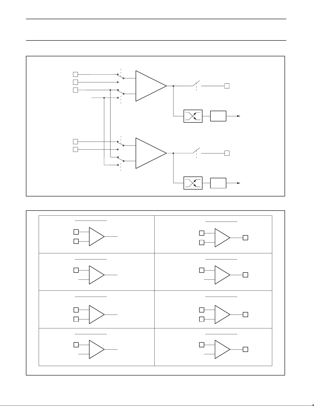
COMPARATOR 1
+
–
COMPARATOR 2
+
(P0.4) CIN1A
(P0.3) CIN1B
(P0.5) CMPREF
(P0.2) CIN2A
(P0.1) CIN2B
CP1
V
ref
CN1
CP2
–
CN2
CO1
CO2
OE1
CHANGE DETECT
OE2
CHANGE DETECT
CMF1
87LPC764
CMP1 (P0.6)
INTERRUPT
CMP2 (P0.0)
CINnA
CMPREF
CINnA
Vref (1.23V)
CINnB
CMPREF
CPn, CNn, OEn = 0 0 0
+
–
CPn, CNn, OEn = 0 1 0
+
–
CPn, CNn, OEn = 1 0 0
+
–
Figure 3. Comparator Input and Output Connections
COn
COn
COn
CINnA
CMPREF
CINnA
V
(1.23V)
ref
CINnB
CMPREF
CMF2
CPn, CNn, OEn = 0 0 1
+
COn
–
CPn, CNn, OEn = 0 1 1
+
COn
–
CPn, CNn, OEn = 1 0 1
+
COn
–
INTERRUPT
SU01153
CMPn
CMPn
CMPn
2000 Apr 14
CPn, CNn, OEn = 1 1 0
CINnB
V
(1.23V) V
ref
+
COn
–
Figure 4. Comparator Configurations
9
CINnB
(1.23V)
ref
CPn, CNn, OEn = 1 1 1
+
COn
–
CMPn
SU01154

Philips Semiconductors Objective specification
Low power, low price, low pin count (20 pin)
microcontroller with 4 kB OTP
Internal Reference Voltage
An internal reference voltage generator may supply a default
reference when a single comparator input pin is used. The value of
the internal reference voltage, referred to as V
Comparator Interrupt
Each comparator has an interrupt flag CMFn contained in its
configuration register . This flag is set whenever the comparator
output changes state. The flag may be polled by software or may be
used to generate an interrupt. The interrupt will be generated when
the corresponding enable bit ECn in the IEN1 register is set and the
interrupt system is enabled via the EA bit in the IEN0 register.
Comparators and Power Reduction Modes
Either or both comparators may remain enabled when Power Down
or Idle mode is activated. The comparators will continue to function
in the power reduction mode. If a comparator interrupt is enabled, a
change of the comparator output state will generate an interrupt and
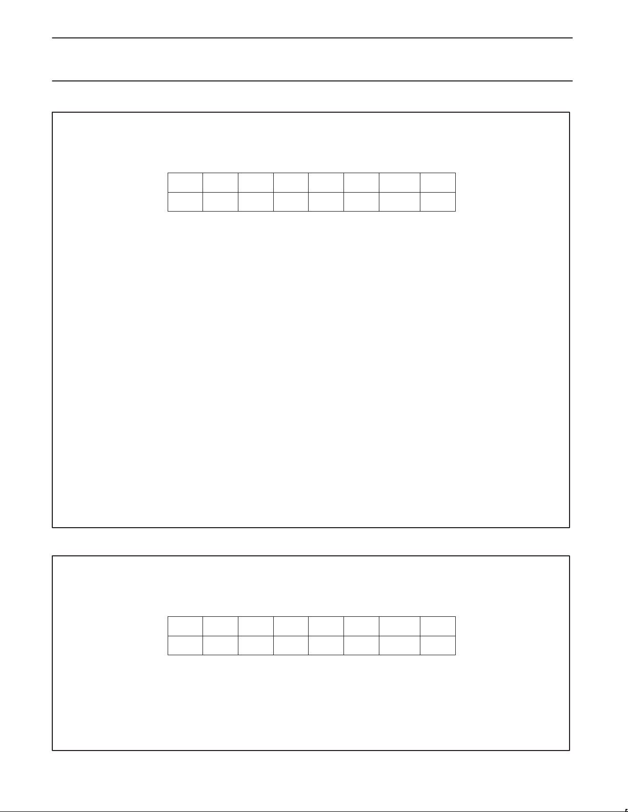
CmpInit:
mov PT0AD,#30h ; Disable digital inputs on pins that are used
anl P0M2,#0cfh ; Disable digital outputs on pins that are used
orl P0M1,#30h ; for analog functions: CIN1A, CMPREF.
mov CMP1,#24h ; Turn on comparator 1 and set up for:
call delay10us ; The comparator has to start up for at
anl CMP1,#0feh ; Clear comparator 1 interrupt flag.
setb EC1 ; Enable the comparator 1 interrupt. The
setb EA ; Enable the interrupt system (if needed).
ret ; Return to caller.
, is 1.28 V ±10%.
ref
; for analog functions: CIN1A, CMPREF.
; – Positive input on CIN1A.
; – Negative input from CMPREF pin.
; – Output to CMP1 pin enabled.
; least 10 microseconds before use.
; priority is left at the current value.
Figure 5.
87LPC764
wake up the processor. If the comparator output to a pin is enabled,
the pin should be configured in the push-pull mode in order to obtain
fast switching times while in power down mode. The reason is that
with the oscillator stopped, the temporary strong pull-up that
normally occurs during switching on a quasi-bidirectional port pin
does not take place.
Comparators consume power in Power Down and Idle modes, as
well as in the normal operating mode. This fact should be taken into
account when system power consumption is an issue.
Comparator Configuration Example
The code shown in Figure 5 is an example of initializing one
comparator. Comparator 1 is configured to use the CIN1A and
CMPREF inputs, outputs the comparator result to the CMP1 pin,
and generates an interrupt when the comparator output changes.
The interrupt routine used for the comparator must clear the
interrupt flag (CMF1 in this case) before returning.
SU01189
2000 Apr 14
10

Philips Semiconductors Objective specification
Low power, low price, low pin count (20 pin)
microcontroller with 4 kB OTP
I2C Serial Interface
The I2C bus uses two wires (SDA and SCL) to transfer information
between devices connected to the bus. The main features of the
bus are:
•Bidirectional data transfer between masters and slaves.
•Serial addressing of slaves (no added wiring).
•Acknowledgment after each transferred byte.
•Multimaster bus.
•Arbitration between simultaneously transmitting masters without
corruption of serial data on bus.
The I2C subsystem includes hardware to simplify the software required
to drive the I
addition to including the necessary arbitration and framing error
checks, includes clock stretching and a bus timeout timer. The
interface is synchronized to software either through polled loops
or interrupts.
Refer to the application note AN422, entitled “Using the 8XC751
Microcontroller as an I
the 8xC76x I
The 87LPC764 I2C implementation duplicates that of the 87C751
and 87C752 except for the following details:
•The interrupt vector addresses for both the I
Timer I interrupt.
•The I
•The location of the I
SFR it is located within (EI2 is Bit 0 in IEN1).
•The location of the Timer I interrupt enable bit and the name of the
SFR it is located within (ETI is Bit 7 in IEN1).
•The I
Timer I is used to both control the timing of the I
detect a “bus locked” condition, by causing an interrupt when
nothing happens on the I
time while a transmission is in progress. If this interrupt occurs, the
program has the opportunity to attempt to correct the fault and
resume I
Six time spans are important in I
•The MINIMUM HIGH time for SCL when this device is the master.
•The MINIMUM LOW time for SCL when this device is a master.
This is not very important for a single-bit hardware interface like
this one, because the SCL low time is stretched until the software
responds to the I2C flags. The software response time normally
meets or exceeds the MIN LO time. In cases where the software
responds within MIN HI + MIN LO) time, timer I will ensure that
the minimum time is met.
•The MINIMUM SCL HIGH TO SDA HIGH time in a stop condition.
•The MINIMUM SDA HIGH TO SDA LOW time between I
and start conditions (4.7ms, see I
•The MINIMUM SDA LOW TO SCL LOW time in a start condition.
•The MAXIMUM SCL CHANGE time while an I
progress. A frame is in progress between a start condition and the
following stop condition. This time span serves to detect a lack of
software response on this device as well as external I2C
2
C bus. The hardware is a single bit interface which in
2
2
C interface and sample driver routines.
2
C SFR addresses (I2CON, !2CFG, I2DAT).
2
C and Timer I interrupts have a settable priority.
2
C operation.
C Bus Master” for additional discussion of
2
C interrupt and the
2
C interrupt enable bit and the name of the
2
C bus and also to
2
C bus for an inordinately long period of
2
C operation and are insured by timer I:
2
C specification).
2
C frame is in
2
C stop
87LPC764
problems. SCL “stuck low” indicates a faulty master or slave. SCL
“stuck high” may mean a faulty device, or that noise induced onto
2
the I
C bus caused all masters to withdraw from I2C arbitration.
The first five of these times are 4.7 ms (see I
are covered by the low order three bits of timer I. Timer I is clocked
by the 87LPC764 CPU clock. Timer I can be pre-loaded with one of
four values to optimize timing for different oscillator frequencies. At
lower frequencies, software response time is increased and will
degrade maximum performance of the I
register I2CFG description for prescale values (CT0, CT1).
The MAXIMUM SCL CHANGE time is important, but its exact span
is not critical. The complete 10 bits of timer I are used to count out
the maximum time. When I
cleared by transitions on the SCL pin. The timer does not run
between I2C frames (i.e., whenever reset or stop occurred more
recently than the last start). When this counter is running, it will carry
out after 1020 to 1023 machine cycles have elapsed since a change
on SCL. A carry out causes a hardware reset of the I
and generates an interrupt if the Timer I interrupt is enabled. In
cases where the bus hang-up is due to a lack of software response
by this device, the reset releases SCL and allows I
among other devices to continue.
Timer I is enabled to run, and will reset the I
overflow, if the TIRUN bit in the I2CFG register is set. The Timer I
interrupt may be enabled via the ETI bit in IEN1, and its priority set
by the PTIH and PTI bits in the Ip1H and IP1 registers respectively.
2
I
C Interrupts
2
C interrupts are enabled (EA and EI2 are both set to 1), an I2C
If I
interrupt will occur whenever the ATN flag is set by a start, stop,
arbitration loss, or data ready condition (refer to the description of ATN
following). In practice, it is not efficient to operate the I
this fashion because the I
have to distinguish between hundreds of possible conditions. Also,
2
sinc e I
C can operate at a fairly high rate, the software may execute
faster if the code simply waits for the I
Typically, the I
condition at an idle slave device, or a stop condition at an idle master
device (if it is waiting to use the I2C bus). This is accomplished by
enabling the I
Reading I2CON
RDAT The data from SDA is captured into “Receive DATa”
ATN “ATteNtion” is 1 when one or more of DRDY, ARL, STR, or
DRDY “Data ReaDY” (and thus ATN) is set when a rising edge
2
C interrupt should only be used to indicate a start
2
C interrupt only during the aforementioned conditions.
whenever a rising edge occurs on SCL. RDAT is also
available (with seven low-order zeros) in the I2DAT
register. The difference between reading it here and
there is that reading I2DAT clears DRDY, allowing the
2
I
C to proceed on to another bit. Typically, the first
seven bits of a received byte are read from
I2DAT, while the 8th is read here. Then I2DAT can be
written to send the Acknowledge bit and clear DRDY.
STP is 1. Thus, ATN comprises a single bit that can be
tested to release the I
occurs on SCL, except at idle slave. DRDY is cleared
by writing CDR = 1, or by writing or reading the I2DAT
register. The following low period on SCL is stretched
until the program responds by clearing DRDY.
2
C operation is enabled, this counter is
2
C interrupt service routine would somehow
2
C service routine from a “wait loop.”
2
C specification) and
2
C bus. See special function
2
C interface
2
C operation
2
C interface upon
2
C interface in
2
C interface.
2000 Apr 14
11
Philips Semiconductors Objective specification
Low power, low price, low pin count (20 pin)
microcontroller with 4 kB OTP
I2CON
Address: D8h
Bit Addressable*
READ
WRITE
BIT SYMBOL FUNCTION
I2CON.7 RDAT Read: the most recently received data bit.
“ CXA Write: clears the transmit active flag.
I2CON.6 ATN Read: ATN = 1 if any of the flags DRDY, ARL, STP, or STP = 1.
2
“ IDLE Write: in the I
is needed again.
I2CON.5 DRDY Read: Data Ready flag, set when there is a rising edge on SCL.
“ CDR Write: writing a 1 to this bit clears the DRDY flag.
I2CON.4 ARL Read: Arbitration Loss flag, set when arbitration is lost while in the transmit mode.
“ CARL Write: writing a 1 to this bit clears the CARL flag.
I2CON.3 STR Read: Start flag, set when a start condition is detected at a master or non-idle slave.
“ CSTR Write: writing a 1 to this bit clears the STR flag.
I2CON.2 STP Read: Stop flag, set when a stop condition is detected at a master or non-idle slave.
“ CSTP Write: writing a 1 to this bit clears the STP flag.
I2CON.1 MASTER Read: indicates whether this device is currently as bus master.
“ XSTR Write: writing a 1 to this bit causes a repeated start condition to be generated.
I2CON.0 — Read: undefined.
“ XSTP Write: writing a 1 to this bit causes a stop condition to be generated.
C slave mode, writing a 1 to this bit causes the I2C hardware to ignore the bus until it
MASTERSTPSTRARLDRDYATNRDAT
87LPC764
Reset Value: 81h
01234567
—
XSTPXSTRCSTPCSTRCARLCDRIDLECXA
* Due to the manner in which bit addressing is implemented in the 80C51 family, the I2CON register should never be altered by
use of the SETB, CLR, CPL, MOV (bit), or JBC instructions. This is due to the fact that read and write functions of this register
are different. Testing of I2CON bits via the JB and JNB instructions is supported.
2
Figure 6. I
I2DAT
Address: D9h
Not Bit Addressable
READ
WRITE
BIT SYMBOL FUNCTION
I2DAT.7 RDAT Read: the most recently received data bit, captured from SDA at every rising edge of SCL. Reading
I2DAT also clears DRDY and the Transmit Active state.
“ XDAT Write: sets the data for the next transmitted bit. Writing I2DAT also clears DRDY and sets the
Transmit Active state.
I2DAT.6–0 – Unused.
Figure 7. I2C Data Register (I2DAT)
C Control Register (I2CON)
Reset Value: xxh
01234567
——————RDAT
—
———————XDAT
SU01155
SU01156
2000 Apr 14
12

Philips Semiconductors Objective specification
Low power, low price, low pin count (20 pin)
microcontroller with 4 kB OTP
Checking ATN and DRDY
When a program detects ATN = 1, it should next check DRDY. If
DRDY = 1, then if it receives the last bit, it should capture the data
from RDAT (in I2DAT or I2CON). Next, if the next bit is to be sent, it
should be written to I2DAT. One way or another, it should clear
DRDY and then return to monitoring ATN. Note that if any of ARL,
STR, or STP is set, clearing DRDY will not release SCL to high, so
that the I
ATN = 1, and DRDY = 0, it should go on to examine ARL, STR,
and STP.
ARL “Arbitration Loss” is 1 when transmit Active was set, but
STR “STaRt” is set to a 1 when an I
STP “SToP” is set to 1 when an I
MASTER “MASTER” is 1 if this device is currently a master on
Writing I2CON
Typically, for each bit in an I
ATN = 1. Based on DRDY, ARL, STR, and STP, and on the current
2
C will not go on to the next bit. If a program detects
this device lost arbitration to another transmitter.
Transmit Active is cleared when ARL is 1. There are
four separate cases in which ARL is set.
1. If the program sent a 1 or repeated start, but another
device sent a 0, or a stop, so that SDA is 0 at the rising
edge of SCL. (If the other device sent a stop, the setting
of ARL will be followed shortly by STP being set.)
2. If the program sent a 1, but another device sent a
repeated start, and it drove SDA low before SCL
could be driven low. (This type of ARL is always
accompanied by STR = 1.)
3. In master mode, if the program sent a repeated start,
but another device sent a 1, and it drove SCL low
before this device could drive SDA low.
4. In master mode, if the program sent stop, but it could
not be sent because another device sent a 0.
2
C start condition is
detected at a non-idle slave or at a master. (STR is not
set when an idle slave becomes active due to a start
bit; the slave has nothing useful to do until the rising
edge of SCL sets DRDY.)
2
C stop condition is
detected at a non-idle slave or at a master. (STP is not
set for a stop condition at an idle slave.)
2
the I
C. MASTER is set when MASTRQ is 1 and the
bus is not busy (i.e., if a start bit hasn’t been
received since reset or a “Timer I” time-out, or if a stop
has been received since the last start). MASTER is
cleared when ARL is set, or after the software writes
MASTRQ = 0 and then XSTP = 1.
2
C message, a service routine waits for
87LPC764
bit position in the message, it may then write I2CON with one or
more of the following bits, or it may read or write the I2DAT register.
CXA Writing a 1 to “Clear Xmit Active” clears the Transmit
Active state. (Reading the I2DAT register also does this.)
Regarding Transmit Active
Transmit Active is set by writing the I2DAT register, or by writing
I2CON with XSTR = 1 or XSTP = 1. The I
the SDA line low when Transmit Active is set, and the ARL bit will
only be set to 1 when Transmit Active is set. Transmit Active is
cleared by reading the I2DAT register, or by writing I2CON with CXA
= 1. Transmit Active is automatically cleared when ARL is 1.
IDLE Writing 1 to “IDLE” causes a slave’s I
ignore the I
2
C until the next start condition (but if
MASTRQ is 1, then a stop condition will cause this
device to become a master).
CDR Writing a 1 to “Clear Data Ready” clears DRDY.
(Reading or writing the I2DAT register also does this.)
CARL Writing a 1 to “Clear Arbitration Loss” clears the ARL bit.
CSTR Writing a 1 to “Clear STaRt” clears the STR bit.
CSTP Writing a 1 to “Clear SToP” clears the STP bit. Note that
if one or more of DRDY, ARL, STR, or STP is 1, the low
time of SCL is stretched until the service routine
responds by clearing them.
XSTR Writing 1s to “Xmit repeated STaRt” and CDR tells the
2
I
C hardware to send a repeated start condition. This
should only be at a master. Note that XSTR need not
and should not be used to send an “initial”
(non-repeated) start; it is sent automatically by the I
hardware. Writing XSTR = 1 includes the effect of
writing I2DA T with XDAT = 1; it sets Transmit Active
and releases SDA to high during the SCL low time.
After SCL goes high, the I
suitable minimum time and then drives SDA low to
make the start condition.
XSTP Writing 1s to “Xmit SToP” and CDR tells the I
hardware to send a stop condition. This should only be
done at a master. If there are no more messages to
initiate, the service routine should clear the MASTRQ
bit in I2CFG to 0 before writing XSTP with 1. Writing
XSTP = 1 includes the effect of writing I2DAT with
XDAT = 0; it sets Transmit Active and drives SDA low
during the SCL low time. After SCL goes high, the I
hardware waits for the suitable minimum time and then
releases SDA to high to make the stop condition.
2
C interface will only drive
2
C hardware to
2
C hardware waits for the
2
C
2
C
2
C
2000 Apr 14
13
Philips Semiconductors Objective specification
Low power, low price, low pin count (20 pin)
microcontroller with 4 kB OTP
I2CFG
Address: C8h
Reset Value: 00h
Not Bit Addressable
01234567
CT1——TIRUNCLRTIMASTRQSLAVEN
CT0
BIT SYMBOL FUNCTION
2
I2CFG.7 SLAVEN Slave Enable. Writing a 1 this bit enables the slave functions of the I
MASTRQ are 0, the I
2
C hardware is disabled. This bit is cleared to 0 by reset and by an I2C
C subsystem. If SLAVEN and
time-out.
I2CFG.6 MASTRQ Master Request. Writing a 1 to this bit requests mastership of the I2C bus. If a transmission is in
progress when this bit is changed from 0 to 1, action is delayed until a stop condition is detected. A
start condition is sent and DRDY is set (thus making ATN = 1 and generating an I
When a master wishes to release mastership status of the I
MASTRQ is cleared by an I
2
C time-out.
2
C, it writes a 1 to XSTP in I2CON.
2
C interrupt).
I2CFG.5 CLRTI Writing a 1 to this bit clears the T imer I overflow flag. This bit position always reads as a 0.
I2CFG.4 TIRUN Writing a 1 to this bit lets Timer I run; a zero stops and clears it. Together with SLAVEN, MASTRQ,
and MASTER, this bit determines operational modes as shown in Table 1.
I2CFG.2, 3 — Reserved for future use. Should not be set to 1 by user programs.
I2CFG.1, 0 CT1, CT0 These two bits are programmed as a function of the CPU clock rate, to optimize the MIN HI and LO
time of SCL when this device is a master on the I
2
C. The time value determined by these bits
controls both of these parameters, and also the timing for stop and start conditions.
87LPC764
2
Figure 8. I
Regarding Software Response Time
Because the 87LPC764 can run at 20 MHz, and because the I
interface is optimized for high-speed operation, it is quite likely that
2
an I
C service routine will sometimes respond to DRDY (which is set
C Configuration Register (I2CFG)
2
C
at a rising edge of SCL) and write I2DAT before SCL has gone low
again. If XDAT were applied directly to SDA, this situation would
produce an I
2
C protocol violation. The programmer need not worry
about this possibility because XDAT is applied to SDA only when
SCL is low.
Conversely, a program that includes an I
a long time to respond to DRDY. Typically, an I
2
C service routine may take
2
C routine operates
on a flag-polling basis during a message, with interrupts from other
peripheral functions enabled. If an interrupt occurs, it will delay the
response of the I
about this very much either, because the I
2
C service routine. The programmer need not worry
2
C hardware stretches the
SCL low time until the service routine responds. The only constraint
on the response is that it must not exceed the Timer I time-out.
Values to be used in the CT1 and CT0 bits are shown in Table 2. To
allow the I
2
C bus to run at the maximum rate for a particular
oscillator frequency , compare the actual oscillator rate to the f OSC
max column in the table. The value for CT1 and CT0 is found in the
SU01157
first line of the table where CPU clock max is greater than or equal
to the actual frequency.
Table 2 also shows the machine cycle count for various settings of
CT1/CT0. This allows calculation of the actual minimum high and
low times for SCL as follows:
SCL min highńlow time (in microseconds) +
6 * Min Time Count
CPU clock (in MHz)
For instance, at an 8 MHz frequency, with CT1/CT0 set to 1 0, the
minimum SCL high and low times will be 5.25 µs.
Table 2 also shows the Timer I timeout period (given in machine
cycles) for each CT1/CT0 combination. The timeout period varies
because of the way in which minimum SCL high and low times are
measured. When the I
2
C interface is operating, Timer I is pre-loaded
at every SCL transition with a value dependent upon CT1/CT0. The
pre-load value is chosen such that a minimum SCL high or low time
has elapsed when Timer I reaches a count of 008 (the actual value
pre-loaded into Timer I is 8 minus the machine cycle count).
2000 Apr 14
14
 Loading...