

Philips P87C592EFA-02, P80C592FHA-00, P80C592FFA-00, P87C592EFL-02, P87C592EFA-A2 Datasheet

DATA SH EET
Product specification
Supersedes data of January 1995
File under Integrated Circuits, IC18
1996 Jun 27
INTEGRATED CIRCUITS
P8xC592
8-bit microcontroller
with on-chip CAN

1996 Jun 27 2
Philips Semiconductors Product specification
8-bit microcontroller with on-chip CAN P8xC592
CONTENTS
1 FEATURES
2 GENERAL DESCRIPTION
3 ORDERING INFORMATION
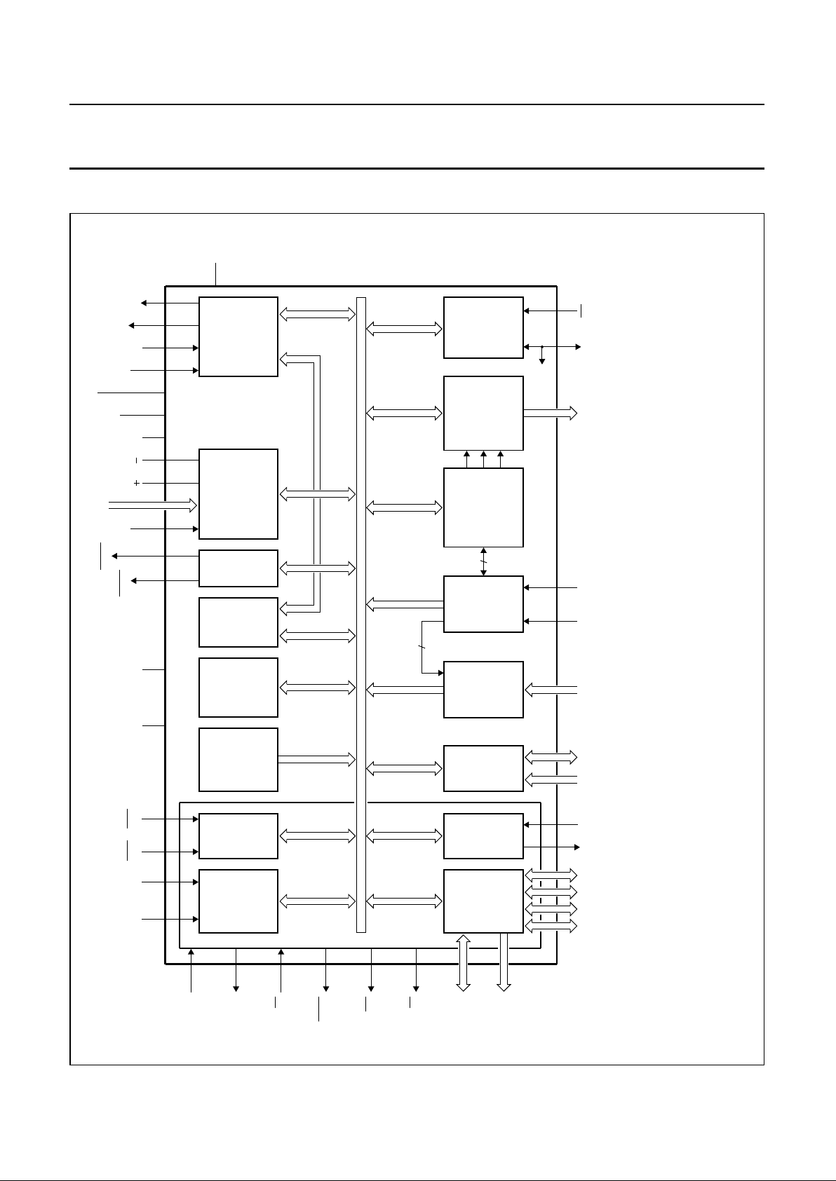
4 BLOCK DIAGRAM
5 PINNING
6 FUNCTIONAL DESCRIPTION
7 MEMORY ORGANIZATION
7.1 Program Memory
7.2 Internal Data Memory
7.3 External Data Memory
8 I/O PORT STRUCTURE
9 PULSE WIDTH MODULATED OUTPUTS
(PWM)
9.1 Prescaler frequency control register (PWMP)
9.2 Pulse Width Register 0 (PWM0)
9.3 Pulse Width Register 1 (PWM1)
10 ANALOG-TO-DIGITAL CONVERTER (ADC)
10.1 ADC Control register (ADCON)
11 TIMERS/COUNTERS
11.1 Timer 0 and Timer 1
11.2 Timer T2 Capture and Compare Logic
11.3 Watchdog Timer (T3)
12 SERIAL I/O PORT: SIO0 (UART)
13 SERIAL I/O PORT: SIO1 (CAN)
13.1 On-chip CAN-controller
13.2 CAN Features
13.3 Interface between CPU and CAN
13.4 Hardware blocks of the CAN-controller
13.5 Control Segment and Message Buffer
description
13.6 CAN 2.0A Protocol description
14 INTERRUPT SYSTEM
14.1 Interrupt Enable and Priority Registers
14.2 Interrupt Vectors
14.3 Interrupt Priority
15 POWER REDUCTION MODES
15.1 Power Control Register (PCON)
15.2 CAN Sleep Mode
15.3 Idle Mode
15.4 Power-down Mode
16 OSCILLATOR CIRCUITRY
17 RESET CIRCUITRY
17.1 Power-on Reset
18 INSTRUCTION SET
18.1 Addressing Modes
18.2 Instruction Set
19 ABSOLUTE MAXIMUM RATINGS (note 1)
20 DC CHARACTERISTICS
21 AC CHARACTERISTICS
22 CAN APPLICATION INFORMATION
22.1 Latency time requirements
22.2 Connecting a P8xC592 to a bus line
(physical layer)
23 PACKAGE OUTLINES
24 SOLDERING
24.1 Introduction
24.2 Reflow soldering
24.3 Wave soldering
24.4 Repairing soldered joints
25 DEFINITIONS
26 LIFE SUPPORT APPLICATIONS

1996 Jun 27 3
Philips Semiconductors Product specification
8-bit microcontroller with on-chip CAN P8xC592
1 FEATURES
• 80C51 central processing unit (CPU)
• 16 kbytes on-chip ROM,
externally expandible to 64 kbytes
• 2 × 256 bytes on-chip RAM,
externally expandible to 64 kbytes
• Two standard 16-bit timers/counters
• One additional 16-bit timer/counter coupled to four
capture and three compare registers
• 10-bit ADC with 8 multiplexed analog inputs
• Two 8-bit resolution Pulse Width Modulated outputs
• 15 interrupt sources with 2 priority levels
(2 to 6 external interrupt sources possible)
• Five 8-bit I/O ports, plus one 8-bit input port shared
with analog inputs
• CAN-controller (CAN = Controller Area Network)
with DMA data transfer facility to internal RAM
• 1 Mbit/s CAN-controller with bus failure
management facility
•1⁄2AVDD reference voltage
• Full-duplex UART compatible with the standard 80C51
• On-chip Watchdog Timer (WDT)
• 1.2 to 16 MHz clock frequency.
2 GENERAL DESCRIPTION
The P8xC592 is a single-chip 8-bit high-performance
microcontroller with on-chip CAN-controller, derived from
the 80C51 microcontroller family.
It uses the powerful 80C51 instruction set.
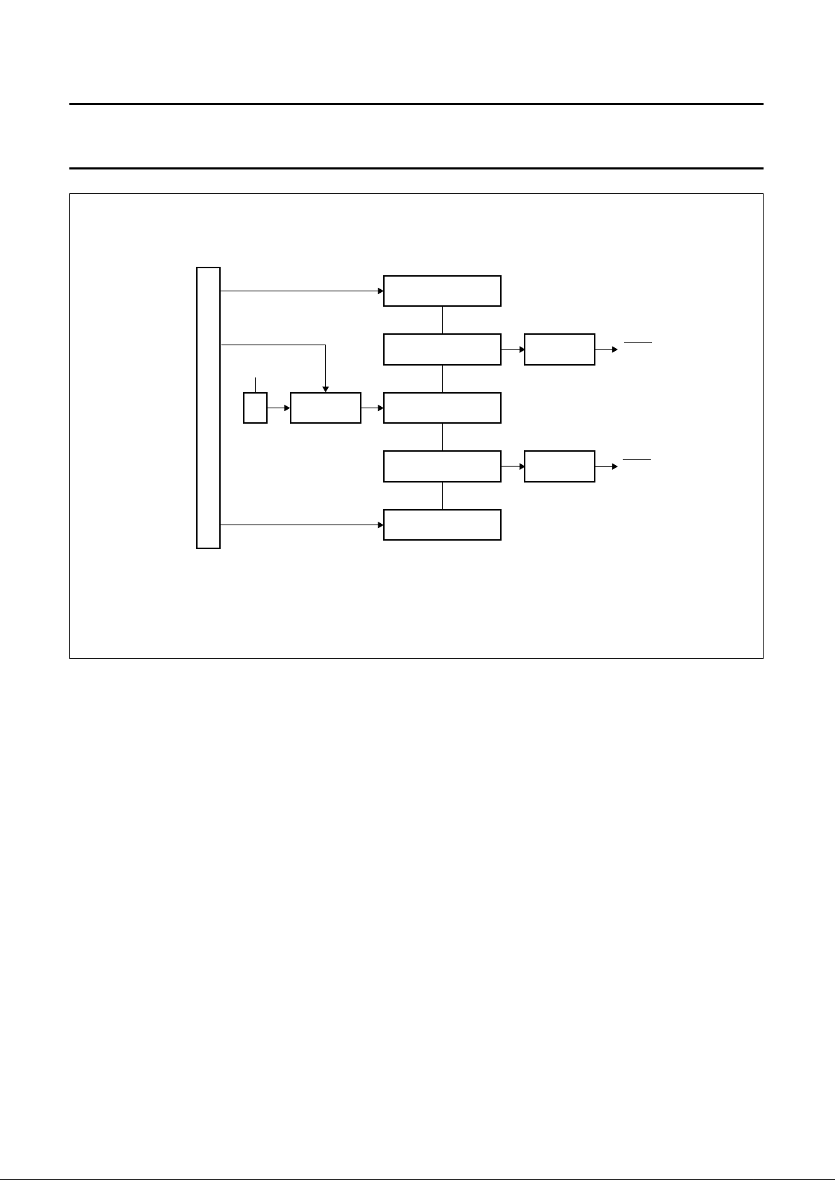
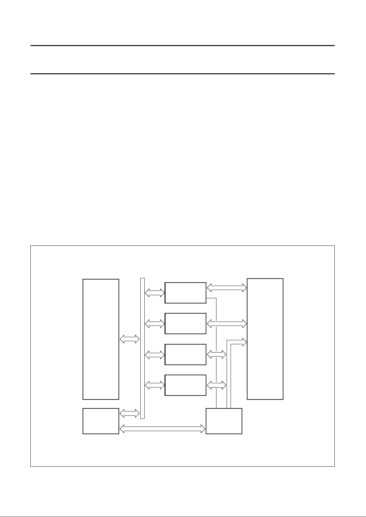
Figure 1 shows a block diagram of the P8xC592.
The P8xC592 is manufactured in an advanced CMOS
process, and is designed for use in automotive and
general industrial applications. In addition to the 80C51
standard features, the device provides a number of
dedicated hardware functions for these applications.
Two versions of the P8xC592 will be offered:
• P80C592 (without ROM)
• P83C592 (with ROM).
Hereafter these versions will be referred to as P8xC592.
The temperature range includes (max. f
CLK
= 16 MHz):
•−40 to +85 °C version, for general applications
•−40 to +125 °C version for automotive applications.
The P8xC592 combines the functions of the P8xC552
(microcontroller) and the PCA82C200 (Philips
CAN-controller) with the following enhanced features:
• 16 kbytes Program Memory
• 2 × 256 bytes Data Memory
• DMA between CAN Transmit/Receive Buffer and
internal RAM.
The main differences between P8xC592 and P8xC552
are:
• 16 kbytes programmable ROM (P8xC552 has 8 kbytes)
• Additional 256 bytes RAM
• A CAN-controller instead of the I2C-serial interface.
3 ORDERING INFORMATION
TYPE
NUMBER
PACKAGE
TEMPERATURE
RANGE (°C)
FREQ.
(MHz)
NAME DESCRIPTION VERSION
Without ROM
P80C592FFA
PLCC68 plastic leaded chip carrier; 68 leads SOT188-2
−40 to +85
1.2 to 16
P80C592FHA −40 to +125
With ROM
P83C592FFA
PLCC68 plastic leaded chip carrier; 68 leads SOT188-2
−40 to +85
1.2 to 16
P83C592FHA −40 to +125
1996 Jun 27 4
Philips Semiconductors Product specification
8-bit microcontroller with on-chip CAN P8xC592
4 BLOCK DIAGRAM
handbook, full pagewidth
handbook, full pagewidth
MGA146
RD
WR
PSEN
XTAL2
XTAL1
A8 to A15
AD0 to AD7
ADC0 to ADC7
EA
CTX1
CTX0CRX0
CRX1
STADC
AV
ref
AV
SS
AV
DD
RST EWCMSR0 to CMSR5
CMT0, CMT1
RT2
T2
P4P5RXDTXDP3P2P1P0
T0
T1 INT0 INT1
V
DD
V
SS
CV
SS
THREE
16-BIT
COMPARATORS
WITH
REGISTERS
PARALLEL
I/O PORTS
&
EXT. BUS
SERIAL
UART
PORT
8-BIT
I/O
PORTS
FOUR
16-BIT
CAPTURE
LATCHES
T2
16-BIT
TIMER/
EVENT
COUNTER
16
16
COMPARATOR
OUTPUT
SELECTION
T3
WATCHDOG
TIMER
T0, T1
TWO 16 - BIT
TIMER/
EVENT
COUNTERS
80C51
core
excluding
ROM/RAM
CPU
PROGRAM
MEMORY
AUXILIARY
MEMORY
DATA
MEMORY
DUAL
PWM
CAN
ADC
DMA - BUS
INTERNAL BUS
P8xC592
REF
16K x 8
ROM
PWM0
PWM1
1/2AV
DD
256 x 8
RAM
256 x 8
RAM
CT0I/INT2 to
CT3I/INT5
(4)
(4) (4) (2) (2) (2) (5)
(6)
(7)
(4)(4)(4)(4) (2) (2)
(4)
(1)
(3)
Fig.1 Block diagram.
(1) Alternative function of Port 0.
(2) Alternative function of Port 1.
(3) Alternative function of Port 2.
(4) Alternative function of Port 3.
(5) Alternative function of Port 4.
(6) Alternative function of Port 5.
(7) Not present in P80C592.
1996 Jun 27 5
Philips Semiconductors Product specification
8-bit microcontroller with on-chip CAN P8xC592
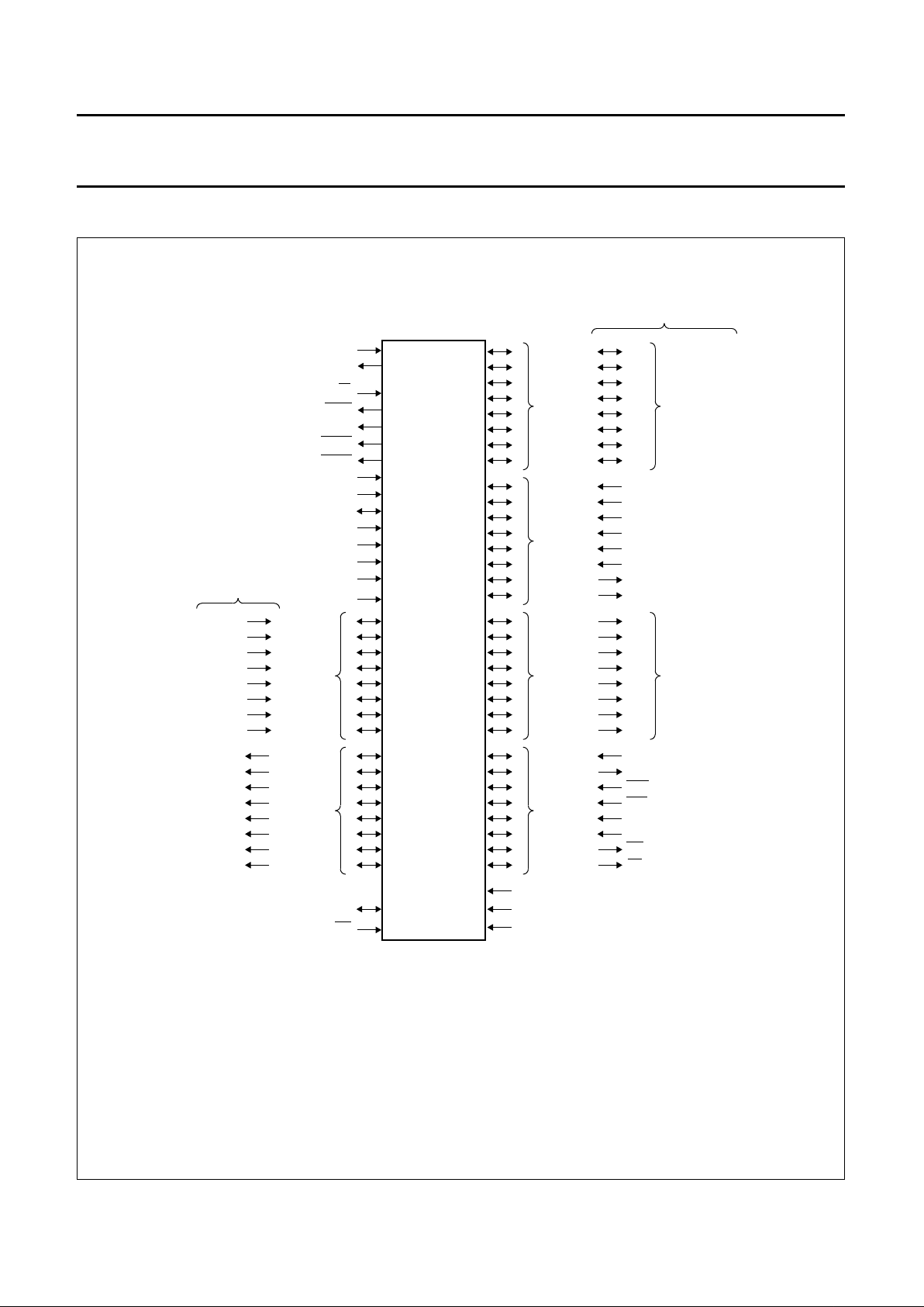
5 PINNING
Fig.2 Pin functions.
handbook, full pagewidth
MGA147 - 2
P8xC592
0
1
2
3
4
5
6
7
PORT 0
CV
SS
SS
V
DD
V
0
1
2
3
4
5
6
7
PORT 1
0
1
2
3
4
5
6
7
PORT 3
AD0
AD1
AD2
AD3
AD4
AD5
AD6
AD7
LOW ORDER
ADDRESS
AND
DATA BUS
alternative function
0
1
2
3
4
5
6
7
PORT 2
A8
A9
A10
A11
A12
A13
A14
A15
HIGH ORDER
ADDRESS
BUS
CT0I/INT2
CT1I/INT3
CT2I/INT4
CT3I/INT5
T2
RT2
CTX0
CTX1
0
1
2
3
4
5
6
7
PORT 5
0
1
2
3
4
5
6
7
PORT 4
RST
EW
alternative function
ADC0
CMSR0
ADC1
ADC2
ADC3
ADC4
ADC5
ADC6
ADC7
CMSR1
CMSR2
CMSR3
CMSR4
CMSR5
CMT0
CMT1
AV
SS
AV
ref+
AV
ref –
STADC
DD
AV
PSEN
CRX0
CRX1
PWM0
PWM1
XTAL1
XTAL2
RXD/DATA
TXD/CLOCK
T0
T1
RD
WR
INT1
INT0
ALE
EA
REF
1996 Jun 27 6
Philips Semiconductors Product specification
8-bit microcontroller with on-chip CAN P8xC592
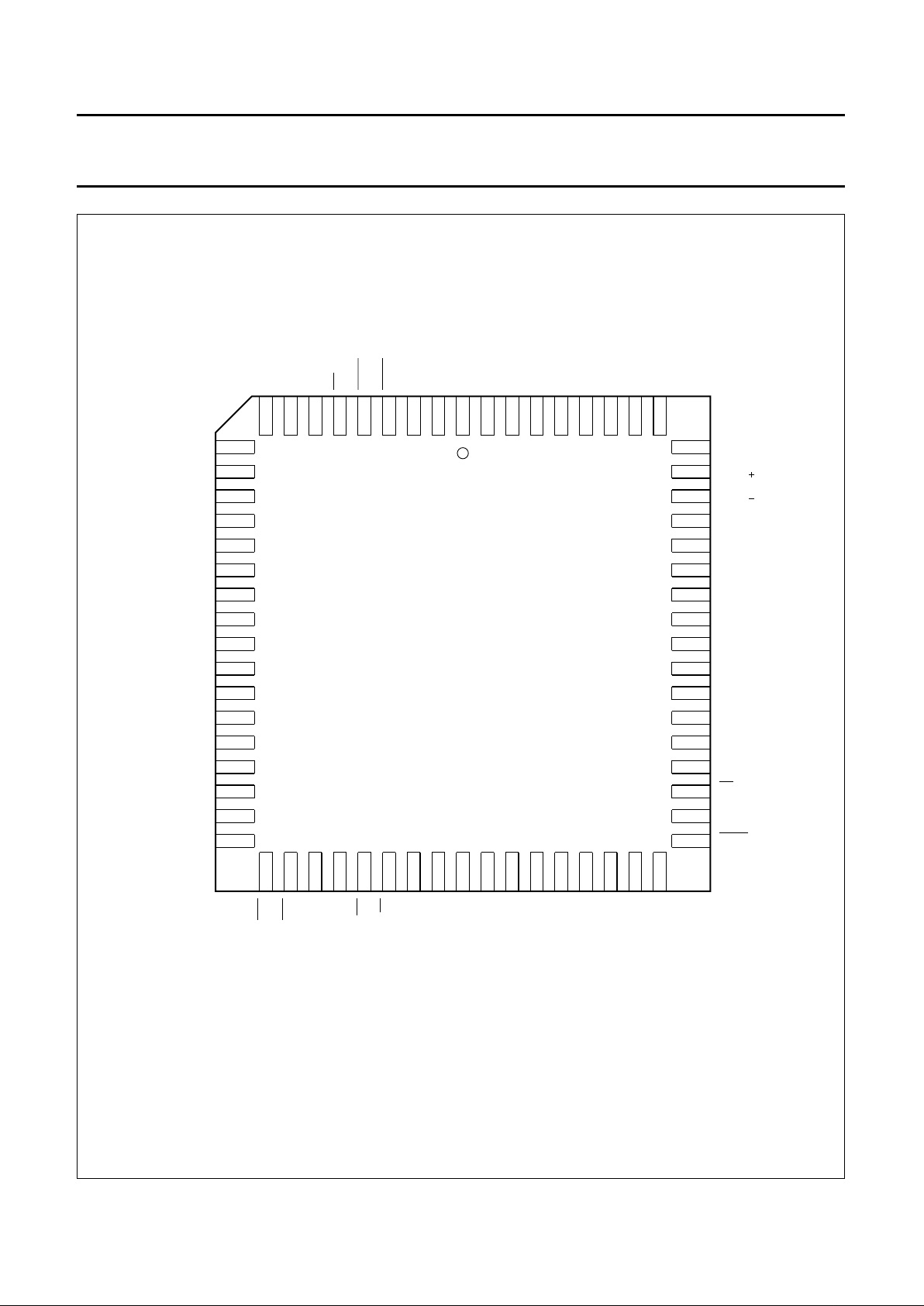
Fig.3 Pin configuration PLCC68/SOT188-2 version (P8xC592FFA; FHA;).
andbook, full pagewidth
P4.3/CMSR3
P4.4/CMSR4
P4.5/CMSR5
P4.6/CMT0
P4.7/CMT1
RST
P1.0/CT0I/INT2
P1.1/CT1I/INT3
P1.2/CT2I/INT4
P1.3/CT3I/INT5
P1.4/T2
P1.5/RT2
CV
SS
P1.6/CTX0
P1.7/CTX1
P3.0/RXD
P3.1/TXD
27
28
29
30
31
32
33
34
35
36
37
38
39
40
41
42
43
9
8
7
6
5
4
3
2
1
68
67
66
65
64
63
62
61
10
11
12
13
14
15
16
17
18
19
20
21
22
23
24
25
26
60
59
58
57
56
55
54
53
52
51
50
49
48
47
46
45
44
P4.2/CMSR2
P4.1/CMSR1
P4.0/CMSR0
EW
PWM1
PWM0
STADC
V
DD
P5.0/ADC0
P5.1/ADC1
P5.2/ADC2
P5.3/ADC3
P5.4/ADC4
P5.5/ADC5
P5.6/ADC6
P5.7/ADC7
AV
DD
P8xC592
MGA148 - 1
AV
SS
CRX0
CRX1
REF
P0.0/AD00
P0.1/AD01
P0.2/AD02
P0.3/AD03
P0.4/AD04
P0.5/AD05
P0.6/AD06
P0.7/AD07
ALE
PSEN
AV
ref
AV
ref
EA
P3.7/RD
XTAL1
P2.3/A11
P3.2/INT0
P3.3/INT1
P3.4/T0
P3.5/T1
P3.6/WR
XTAL2
P2.0/A08
P2.1/A09
P2.2/A10
P2.4/A12
P2.5/A13
P2.6/A14
P2.7/A15
V
SS

1996 Jun 27 7
Philips Semiconductors Product specification
8-bit microcontroller with on-chip CAN P8xC592
Table 1 Pin description for single function pins (SOT188-2; see note 1)
Notes
1. To avoid a ‘latch up’ effect at power-on: VSS− 0.5 V < ‘voltage on any pin at any time’ < VDD+ 0.5 V.
2. Triggered by a rising edge. ADC operation can also be started by software.
3. RST also provides a reset pulse as output when timer T3 overflows or after a CAN wake-up from Power-down.
4. ALE is activated every six oscillator periods. During an external data memory access one ALE pulse is skipped.
5. See Section 7.1, Table 3 for EA operation. For P83Cxxx microcontrollers specified with the option ‘ROM-code
protection’, the EA pin is latched during reset and is ‘don't care’ after reset, regardless of whether the ROM-code
protection is selected or not.
SYMBOL PIN DESCRIPTION
V
DD
2 Power supply, digital part (+5 V). For normal operation and power reduced modes.
STADC 3 Start ADC operation. Input starting analog-to-digital conversion (note 2). This pin must not float.
PWM0 4 Pulse width modulation output 0.
PMW1 5 Pulse width modulation output 1.
EW 6 Enable Watchdog Timer (WDT): enable for T3 Watchdog Timer and disable Power-down mode.
This pin must not float.
RST 15 Reset: input to reset the P8xC592 (note 3).
CV
SS
22 CAN ground potential for the CAN transmitter outputs.
XTAL2 33 Crystal pin 2: output of the inverting amplifier that forms the oscillator.
When an external clock oscillator is used this pin is left open-circuit.
XTAL1 34 Crystal pin 1: input to the inverting amplifier that forms the oscillator, and input to the internal clock
generator. Receives the external clock oscillator signal, when an external oscillator is used.
V
SS
35 Ground, digital part.
PSEN 44 Program Store Enable: Read strobe to external Program Memory (active LOW).
Drive: 8 × LSTTL inputs.
ALE 45 Address Latch Enable: latches the Low-byte of the address during accesses to external memory
(note 4). Drive: 8 × LSTTL inputs; handles CMOS inputs without an external pull-up.
EA 46 External Access input. See note 5.
REF 55
1
⁄2AVDD reference voltage output respectively input (note 6).
CRX1 56 Inputs from the CAN-bus line to the differential input comparator of the on-chip CAN-controller
(note 7).
CRX0 57
AV
REF−
58 Low-end of ADC (analog-to-digital) conversion reference resistor.
AV
REF+
59 High-end of ADC (analog-to-digital) conversion reference resistor (note 8).
AV
SS
60 Ground, analog part. For ADC, CAN receiver and reference voltage.
AV
DD
61 Power supply, analog part (+5 V). For ADC, CAN receiver and reference voltage.
1996 Jun 27 8
Philips Semiconductors Product specification
8-bit microcontroller with on-chip CAN P8xC592
6. Pin 55, REF:
a) Selection of input resp. output dependent of CAN Control Register bit 5 (CR.5; see Section 13.5.3 Table 32).
b) If the internal reference is used, then REF should be connected to AVSS via a capacitor with a value of ≥10 nF.
c) After an external reset (RST = HIGH) the internal1⁄2AVDD source is activated and, REF is a reference output.
d) If the CAN-controller is in the reset state, e.g. after an external reset, then the1⁄2AVDD source is switched off
during Power-down mode.
7. CAN-bus line:
a) CRX0 level > CRX1 level is interpreted as a logic 1 (recessive).
b) CRX0 level < CRX1 level is interpreted as a logic 0 (dominant).
8. The level of AV
REF+
must be higher than that of AV
REF−
.
Table 2 Pin description for pins with alternative functions (SOT188-2 and NO330; see note 1)
SYMBOL
PIN DESCRIPTION
DEFAULT ALTERNATIVE
Port 4
P4.0 to P4.7 7 to 14 8-bit quasi-bidirectional I/O port.
CMSR0 7 Compare and Set/Reset outputs for Timer T2.
CMSR1 8
CMSR2 9
CMSR3 10
CMSR4 11
CMSR5 12
CMT0 13 Compare and toggle outputs for Timer T2.
CMT1 14
Port 1
P1.0 to P1.7 16 to 21, 23, 24 8-bit quasi-bidirectional I/O port.
CT0I/INT2 16 Capture timer inputs for Timer T2,
or
External interrupt inputs.
CT1I/INT3 17
CT2I/INT4 18
CT3I/INT5 19
T2 20 T2 event input (rising edge triggered).
RT2 21 T2 timer reset input (rising edge triggered).
CTX0 23 CAN transmitter output 0 (note 2).
CTX1 24 CAN transmitter output 1 (note 2).
1996 Jun 27 9
Philips Semiconductors Product specification
8-bit microcontroller with on-chip CAN P8xC592
Notes
1. To avoid a ‘latch up’ effect at power-on: VSS− 0.5 V < ‘voltage on any pin at any time’ < VDD+ 0.5 V.
2. If the CAN-controller is in the reset state (e.g. after a power-up reset; CAN Control Register bit CR.0; see
Section 13.5.3 Table 32), the CAN transmitter outputs are floating and the pins P1.6 and P1.7 can be used as
open-drain port pins. After a power-up reset the port data is HIGH, leaving the pins P1.6 and P1.7 floating.
Port 3
P3.0 to P3.7 25 to 32 8-bit quasi-bidirectional I/O port.
RXD 25 Serial Input Port.
TXD 26 Serial Output Port.
INT0 27 External interrupt inputs.
INT1 28
T0 29 Timer 0 external input.
T1 30 Timer 1 external input.
WR 31 External Data Memory Write strobe.
RD 32 External Data Memory Read strobe.
Port 2 (Sink/source: 1 × TTL = 4 × LSTTL inputs)
P2.0 to P2.7 36 to 43 8-bit quasi-bidirectional I/O port.
A08 to A15 High-order address byte for external memory.
Port 0 (Sink/source: 8 × LSTTL inputs)
P0.7 to P0.0 47 to 54 8-bit open drain bidirectional I/O port.
AD7 to AD0 Multiplexed Low-order address and
Data bus for external memory.
Port 5
P5.7 to P5.0 62 to 68, 1 8-bit input port.
ADC7 to ADC0 8 input channels to ADC.
SYMBOL
PIN DESCRIPTION
DEFAULT ALTERNATIVE

1996 Jun 27 10
Philips Semiconductors Product specification
8-bit microcontroller with on-chip CAN P8xC592
6 FUNCTIONAL DESCRIPTION
The P8xC592 functions will be described as shown in the
following overview:
• Memory organization
• I/O Port structure
• Pulse Width Modulated outputs
• Analog-to-digital Converter
• Timers/Counters
• Serial I/O Ports
• Interrupt system
• Power reduction modes
• Oscillator circuitry
• Reset circuitry
• Instruction Set.
7 MEMORY ORGANIZATION
The Central Processing Unit (CPU) manipulates operands
in three memory spaces (see Fig.4) as follows:
• 16 kbytes internal resp. 64 kbytes external Program
Memory
• 512 bytes internal Data Memory MAIN- and AUXILIARY
RAM
• up to 64 kbytes external Data Memory
(with 256 bytes residing in the internal AUXILIARY
RAM).
handbook, full pagewidth
MGA149
INDIRECT ONLY
DIRECT AND
INDIRECT
AUXILIARY
RAM
SFRs
255
127
0
EXTERNAL
(EA = 0)
INTERNAL
(EA = 1)
MAIN RAM
INTERNAL DATA MEMORY
EXTERNAL
DATA MEMORY
PROGRAM MEMORY
EXTERNAL
64K
64K
16384
16383
0
OVERLAPPED SPACE
256
Fig.4 Memory map.
1996 Jun 27 11
Philips Semiconductors Product specification
8-bit microcontroller with on-chip CAN P8xC592
7.1 Program Memory
The Program Memory of the P8xC592 consists of 16 kbytes ROM on-chip, externally expandible up to 64 kbytes.
Table 3 Instruction fetch controlled by
EA
Notes
1. This implementation prevents reading of the internal program code by switching from external Program Memory
during a MOVC instruction.
2. By setting a security bit the internal Program Memory content is protected, which means it cannot be read out.
If the security bit has been set to LOW there are no restrictions for the MOVC instruction.
7.2 Internal Data Memory
The internal Data Memory is physically built-up and accessible as shown in Table 4 (see Fig.5).
Table 4 Internal Data Memory size and address mode
Notes
1. MAIN RAM can be addressed directly and indirectly as in the 80C51.
2. AUXILIARY RAM (0 to 255):
a) Is indirectly addressable in the same way as the external Data Memory with MOVX instructions.
b) Access will not affect the ports P0, P2, P3.6 and P3.7 during internal program execution.
3. SFRs = Special Function Registers.
PIN EA (note 1)
INSTRUCTIONS FETCHED FROM:
ADDRESS
LOCATION
DURING RESET
LATCHED TO:
AFTER RESET
H − internal Program Memory (note 2) 0000H → 3FFFH
H − external Program Memory 4000H → FFFFH
L − 0000H → FFFFH
− ‘don’t care’ −−
INTERNAL
DATA MEMORY
SIZE LOCATION
ADDRESS MODE
POINTERS
DIRECT INDIRECT
MAIN RAM
(note 1)
256 bytes 0 to 127 X X address pointers are R0 and R1 of the
selected register bank
128 to 255 − X
AUXILIARY RAM
(note 2)
256 bytes 0 to 255 − X address pointers are R0 and R1 of the
selected register bank and the DPTR
SFRs (note 3) 128 bytes 128 to 255 X −−
1996 Jun 27 12
Philips Semiconductors Product specification
8-bit microcontroller with on-chip CAN P8xC592
7.2.1 MAIN RAM
Four 8-bit register banks occupy the lower RAM area,
• BANK 0: location 0 to 7
• BANK 1: location 8 to 15
• BANK 2: location 16 to 23
• BANK 4: location 24 to 31.
Only one of these banks may be enabled at the same time.
The next 16 bytes, locations 32 through 45, contains
128 directly addressable bit locations.
The stack can be located anywhere in the internal MAIN
RAM address space. The stack depth is only limited by the
internal RAM space available. All registers except the
program counter and the four 8-bit register banks reside in
the SFR address space.
MGA152
7F 7E 7D 7C 7B 7A 79 78
77 76 75 74 73 72 71 70
6F 6E 6D 6C 6B 6A 69 68
67 66 65 64 63 62 61 60
5F 5E 5D 5C 5B 5A 59 58
57 56 55 54 53 52 51 50
4F 4E 4D 4C 4B 4A 49 48
47 46 45 44 43 42 41 40
3F 3E 3D 3C 3B 3A 39 38
37 36 35 34 33 32 31 30
2F 2E 2D 2C 2B 2A 29 28
27 26 25 24 23 22 21 20
1F 1E 1D 1C 1B 1A 19 18
17 16 15 14 13 12 11 10
0F 0E 0D 0C 0B 0A 09 08
07 06 05 04 03 02 01 00
18H
17H
10H
0FH
08H
07H
00H
24
23
31
16
15
8
7
0
BANK 0
BANK 1
BANK 2
BANK 3
32
33
34
35
36
37
38
39
40
41
42
43
44
45
46
47
(MSB) (LSB)
127
7FH
2FH
2EH
2DH
2CH
2BH
2AH
29H
28H
27H
26H
25H
24H
23H
22H
21H
20H
1FH
Fig.5 Internal MAIN RAM bit addresses.
7.3 External Data Memory
An access to external Data Memory locations higher than
255 will be performed with the MOVX @DPTR instructions
in the same way as in the 80C51 structure,
i.e. with P0 and P2 as data/address bus and P3.6 and P3.7
as Write and Read strobe signals.
Note that these external Data Memory locations cannot be
accessed with R0 or R1 as address pointer.
1996 Jun 27 13
Philips Semiconductors Product specification
8-bit microcontroller with on-chip CAN P8xC592
Fig.6 Special Function Register memory map (a).
handbook, full pagewidth
MGA150
FEFF FD FC FB FA F9 F8
F6F7 F5 F4 F3 F2 F1 F0
EEEF ED EC EB EA E9 E8
E6E7 E5 E4 E3 E2 E1 E0
DEDF DD DC DB DA D9 D8
D6D7 D5 D4 D3 D2 D1 D0
CECF CD CC CB CA C9 C8
C6C7 C5 C4 C3 C2 C1 C0
BIT ADDRESS
REGISTER
MNEMONIC
FFH
DIRECT
BYTE
ADDRESS (HEX)
FEH
FDH
FCH
F8H
F0H
EFH
EEH
EDH
ECH
EBH
EAH
E8H
E0H
DBH
DAH
D9H
D8H
D0H
CFH
CEH
CDH
CCH
CBH
CAH
C9H
C8H
C6H
C5H
C4H
C0H
SFRs containing
directly addressable
bits
T3
PWMP
PWM1
PWM0
IP1
B
RTE
STE
# TMH2
# TML2
CTCON
TM2CON
IEN1
ACC
CANADR
CANDAT
CANCON
CANSTA
PSW
# CTH3
# CTH2
# CTH1
# CTH0
CMH2
CMH1
CMH0
TM2IR
# ADCH
ADCON
# P5
P4
# denotes read-only registers
1996 Jun 27 14
Philips Semiconductors Product specification
8-bit microcontroller with on-chip CAN P8xC592
Fig.7 Special Function Register memory map (b).
handbook, full pagewidth
MGA151
BEBF BD BC BB BA B9 B8
B6B7 B5 B4 B3 B2 B1 B0
AEAF AD AC AB AA A9 A8
A6A7 A5 A4 A3 A2 A1 A0
9E9F 9D 9C 9B 9A 99 98
9697 95 94 93 92 91 90
8E8F 8D 8C 8B 8A 89 88
8687 85 84 83 82 81 80
BIT ADDRESS
REGISTER
MNEMONIC
DIRECT
BYTE
ADDRESS (HEX)
B8H
B0H
AFH
AEH
ADH
ACH
ABH
AAH
A8H
A0H
99H
98H
90H
8DH
8CH
8BH
8AH
89H
88H
87H
83H
82H
81H
80H
SFRs containing
directly addressable
bits
IP0
P3
# CTL3
P2
S0BUF
S0CON
P1
TH1
TH0
TL1
TL0
TMOD
PCON
DPH
DPL
SP
P0
# denotes read-only registers
# CTL2
# CTL1
# CTL0
CML2
CML1
CML0
IEN0
TCON
A9H
1996 Jun 27 15
Philips Semiconductors Product specification
8-bit microcontroller with on-chip CAN P8xC592
8 I/O PORT STRUCTURE
The P8xC592 has six 8-bit parallel ports: Port 0 to Port 5. In addition to the standard 8-bit parallel ports, the I/O facilities
also include a number of special I/O lines. The use of a Port 1, Port 3 or Port 4 pins as an alternative function is carried
out automatically provided the associated SFR bit is set HIGH.
Table 5 Default Port functions
Table 6 Alternative Port functions
PORT TYPE FUNCTION REMARKS
Port 0 I/O The same as in the 80C51 Except for the additional functions of P1.6 and
P1.7.
Port 1 I/O
Port 2 I/O
Port 3 I/O
Port 4 I/O Parallel l/O port Parallel I/O function is identical to Port1, 2 and 3.
Port 5 I Parallel input port with an input function only May be used as normal inputs if the ADC function
is inoperative.
PORT TYPE FUNCTION REMARKS
Port 0 I/O Multiplexed Low-order address and
Data bus for external memory (AD7 to AD0)
Provides the multiplexed Low-order address and
data bus used for expanding the P8xC592 with
standard memories and peripherals.
Port 1 I/O Capture timer inputs for Timer T2
(CT0I to CT3I), or
External interrupt request inputs
(INT2 to INT5)
External interrupt request inputs, if capture
information is not utilized.
T2 event input (T2) External counter input.
T2 timer reset input (RT2) External counter reset input.
CAN transmitter output 0 (CTX0) CTX0 and CTX1 outputs of the CAN interface
(note 1).
CAN transmitter output 1 (CTX1)
Port 2 I/O High-order address byte for external memory
(A08 to A15)
Port 2 provides the High-order address bus when
the P8xC592 is expanded with external Program
Memory and/or external Data Memory.
Port 3 I/O Serial Input Port (RXD) Receiver input of serial port SIO0 (UART).
Serial Output Port (TXD) Transmitter output of serial port SIO0 (UART).
External interrupt (
INT0) External interrupt request inputs.
External interrupt (
INT1)
Timer 0 external input (T0) Counter inputs.
Timer 1 external input (T1)
External data memory Write strobe (
WR) Control signal to write to external Data Memory.
External data memory Read strobe (
RD) Control signal to read from external Data Memory.
Port 4 I/O Compare and Set/Reset outputs
(CMSR0 to CMSR5)
Can be configured to provide signals indicating a
match between Timer counter T2 and its compare
registers.
Compare and toggle outputs (CMT0, CMT1)
Port 5 I Input channels to ADC (ADC7 to ADC0) Port 5 may be used in conjunction with the ADC
interface (note 2).
1996 Jun 27 16
Philips Semiconductors Product specification
8-bit microcontroller with on-chip CAN P8xC592
Notes to the alternative Port functions
1. Port lines P1.6 and P1.7 may be selected as CTX0 and CTX1 outputs of the serial port SIO1 (CAN).
After reset P1.6 and P1.7 may be used as normal I/O ports, if the CAN interface is not used.
2. Unused analog inputs can be used as digital inputs. As Port 5 lines may be used as inputs to the ADC, these digital
inputs have an inherent hysteresis to prevent the input logic from drawing too much current from the power lines
when driven by analog signals.
Channel-to-channel crosstalk should be taken into consideration when both digital and analog signals are
simultaneously input to Port 5 (see Chapter 20).
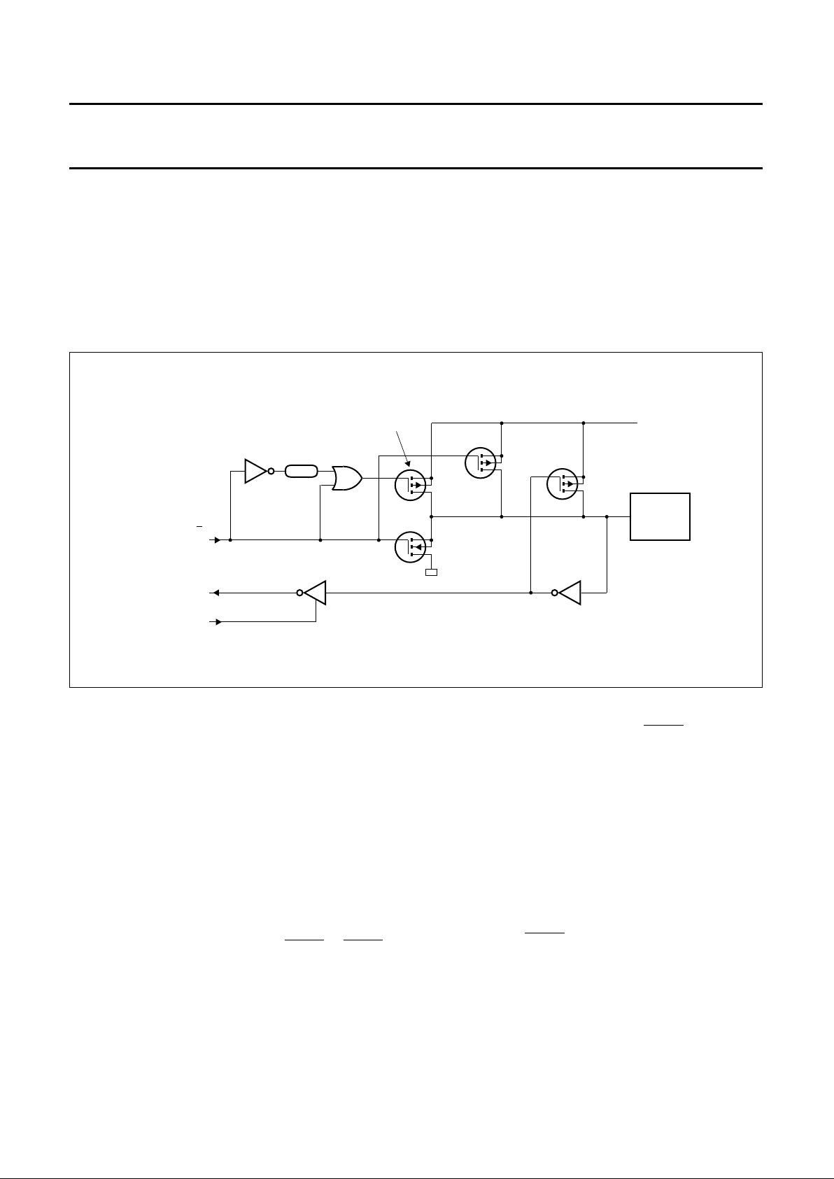
Fig.8 I/O buffers in the P8xC592 (P1.0 to P1.5, Ports 2, 3, and 4).
handbook, full pagewidth
MGA153
p1
p2
p3
input data
read port pin
2 oscillator
periods
n
strong pull-up
I/O PIN
PORT
1, 2, 3 or 4
+5 V
I1
Q
from port latch
INPUT
BUFFER
9 PULSE WIDTH MODULATED OUTPUTS (PWM)
Two Pulse Width Modulated (PWM) output channels are
available with the P8xC592. These channels provide
output pulses of programmable length and interval.
The repetition frequency is defined by an 8-bit prescaler
PWMP which generates the clock for the counter.
Both the prescaler and counter are common to both PWM
channels. The 8-bit counter counts modulo 255 i.e. from
0 to 254 inclusive. The value of the 8-bit counter is
compared to the contents of two registers:
PWM0 and PWM1.
Provided the contents of either of these registers is greater
than the counter value, the output of PWM0 or PWM1 is
set LOW. If the contents of these register are equal to, or
less than the counter value, the output will be HIGH. The
pulse-width-ratio is therefore defined by the contents of the
register PWM0 and PWM1. The pulse-width-ratio is in the
range of 0 to
255
⁄
255
and may be programmed in
increments of1⁄
255
.
The repetition frequency f
PWM
, at the PWMn outputs is
given by:
When using an oscillator frequency of 16 MHz, for
example, the above formula would give a repetition
frequency range of 123 Hz to 31.4 kHz.
By loading the PWM registers with either 00H or FFH, the
PWM outputs can be retained at a constant HIGH or LOW
level respectively. When loading FFH to the PWM
registers, the 8-bit counter will never actually reach this
(FFH) value.
Both output pins
PWMn are driven by push-pull drivers,
and are not shared with any other function.
f
PWM
f
CLK
2 PWMP 1+()× 255×
--------------------------------------------------------------
=
1996 Jun 27 17
Philips Semiconductors Product specification
8-bit microcontroller with on-chip CAN P8xC592
9.1 Prescaler frequency control register (PWMP)
Table 7 Prescaler frequency control register (address FEH)
Table 8 Description of PWMP bits
9.2 Pulse Width Register 0 (PWM0)
Table 9 Pulse Width Register (address FCH)
Table 10 Description of PWM0 bits
9.3 Pulse Width Register 1 (PWM1)
Table 11 Pulse width register (address FDH)
Table 12 Description of PWM1 bits
76543210
PWMP.7 PWMP.6 PWMP.5 PWMP.4 PWMP.3 PWMP.2 PWMP.1 PWMP.0
BIT SYMBOL FUNCTION
7
to
0
PWMP.7
to
PWMP.0
Prescaler division factor.
The Prescaler division factor = (PWMP) + 1.
76543210
PWM0.7 PWM0.6 PWM0.5 PWM0.4 PWM0.3 PWM0.2 PWM0.1 PWM0.0
BIT SYMBOL FUNCTION
7
to
0
PWM0.7
to
PWM0.0
Pulse width ratio.
76543210
PWM1.7 PWM1.6 PWM1.5 PWM1.4 PWM1.3 PWM1.2 PWM1.1 PWM1.0
BIT SYMBOL FUNCTION
7
to
0
PWM1.7
to
PWM1.0
Pulse width ratio.
LOW/HIGH ratio of PWMn signals
PWMn()
255 PWMn()–
----------------------------------------- -
=
LOW/HIGH ratio of PWMn signals
PWMn()
255 PWMn()–
----------------------------------------- -
=
1996 Jun 27 18
Philips Semiconductors Product specification
8-bit microcontroller with on-chip CAN P8xC592
Fig.9 Functional diagram of Pulse Width Modulated outputs.
handbook, full pagewidth
MGA154
I
N
T
E
R
N
A
L
B
U
S
f
clk
PWMP
PWM1
PRESCALER
8-BIT COUNTER1/2
PWM0
8-BIT COMPARATOR
8-BIT COMPARATOR
OUTPUT
BUFFER
PWM1
OUTPUT
BUFFER
PWM0
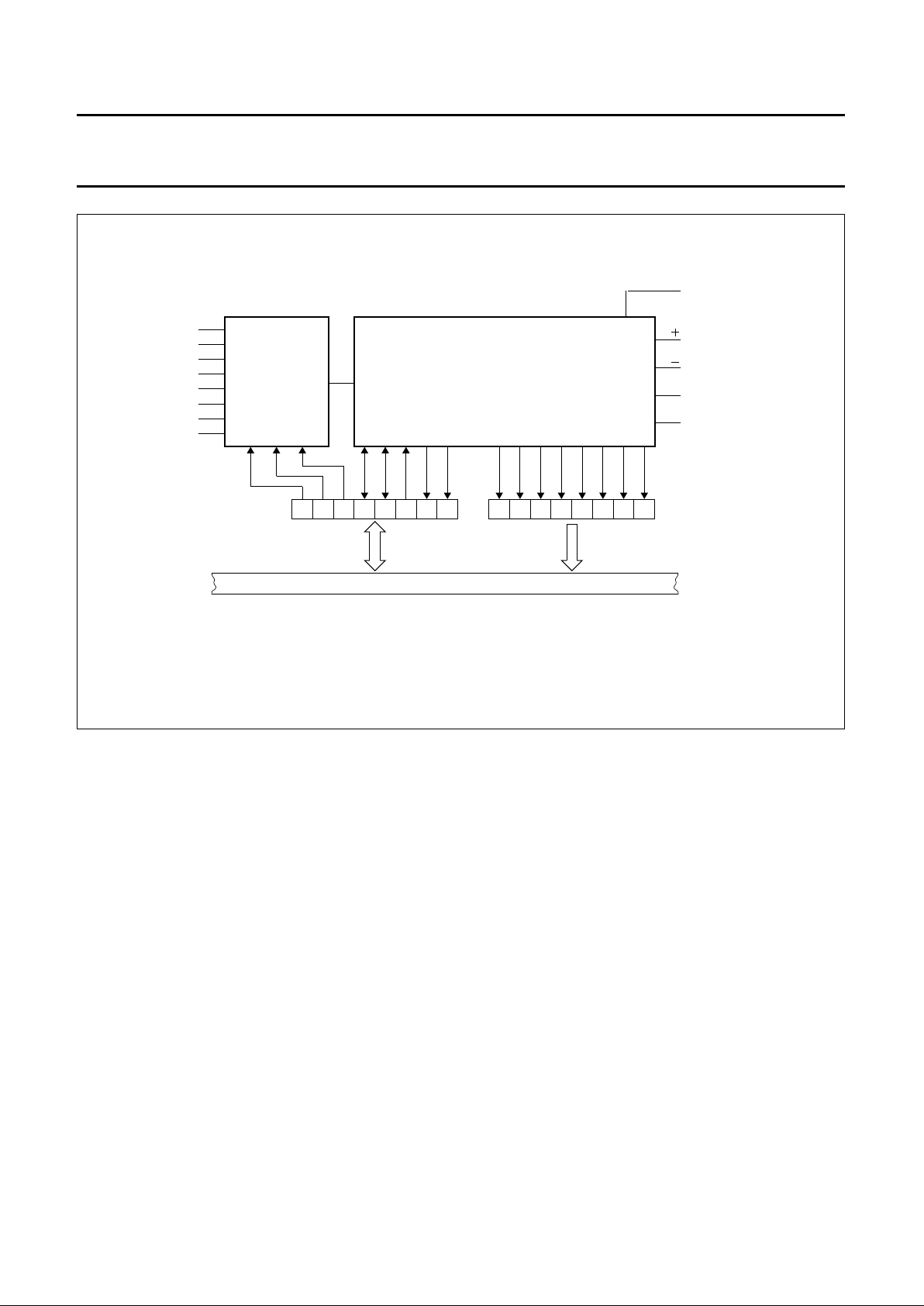
10 ANALOG-TO-DIGITAL CONVERTER (ADC)
The analog input circuitry consists of an 8-input analog
multiplexer and an ADC with 10-bit resolution. The analog
reference voltage and analog power supplies are
connected via separate input pins. The conversion takes
50 machine cycles i.e. 37.5 µs at 16 MHz oscillator
frequency. The input voltage swing is from 0 V to AVDD.
The ADC is controlled using the ADCON control register.
Register bits ADCON.0 to ADCON.2 select the input
channels of the analog multiplexer (see Fig.10).
The completion of the 10-bit analog-to-digital conversion is
flagged by ADCI in the ADCON register and the result is
stored in the SFR ADCH (upper 8-bits) and the 2 lower bits
(ADC.1 and ADC.0) in register ADCON.
An analog-to-digital conversion in progress is unaffected
by an external or software ADC start. The result of a
completed conversion remains unchanged provided
ADCI = HIGH. While ADCI or ADCS are HIGH, a new ADC
START will be blocked and consequently lost. An
analog-to-digital conversion already in progress is aborted
when the Idle or Power-down mode is entered.
The result of a completed conversion (ADCI = HIGH)
remains unaffected during the Idle mode.
The LOW-to-HIGH transition of STADC is recognized at
the end of a machine cycle and the conversion
commences at the beginning of the next cycle. When a
conversion is initiated by software, the conversion starts at
the beginning of the machine cycle following the
instruction that sets ADCS.
The next two machine cycles are used to initiate the
converter. At the end of this first cycle, the ADCS status
flag is set to HIGH while the conversion is in progress.
Sampling of the analog input commences at the end of the
second cycle.
During the next eight machine cycles, the voltage at the
previously selected pin of Port 5 is sampled and this input
voltage should be stable in order to obtain a useful sample.
In any case, the input voltage slew rate must be less than
10 V/ms (5 V conversion range) in order to prevent an
undefined result. The conversion takes four machine
cycles per bit.
1996 Jun 27 19
Philips Semiconductors Product specification
8-bit microcontroller with on-chip CAN P8xC592
10.1 ADC Control register (ADCON)
Table 13 ADC Control register (address C5H)
Table 14 Description of the ADCON bits
Table 15 ADCI and ADCS operating modes
If ADCI is cleared by software while ADCS is set at the same time a new analog-to-digital conversion with the same
channel-number may be started. It is recommended to reset ADCI before ADCS is set.
Note
1. Start of a new conversion requires ADCI = 0.
76543210
ADC.1 ADC.0 ADEX ADCI ADCS AADR2 AADR1 AADR0
BIT SYMBOL FUNCTION
7 ADC.1 Bit 1 of ADC converted value.
6 ADC.0 Bit 0 of ADC converted value.
5 ADEX Enable external start of conversion by STADC. If ADEX is:
LOW, then conversion cannot be started externally by STADC (only by software by setting ADCS)
HIGH, then conversion can be started externally by a rising edge on STADC or externally.
4 ADCI ADC interrupt flag. This flag is set when an analog-to-digital conversion result is ready to be read.
If enabled, an interrupt is invoked. The flag must be cleared by software.
It cannot be set by software (see Table 15).
3 ADCS ADC start and status. Setting this bit starts an analog-to-digital conversion. It may be set by
software or by the external signal STADC. The ADC logic ensures that this signal is HIGH while the
ADC is busy. On completion of the conversion, ADCS is reset at the same time the interrupt flag
ADCI is set. ADCS can not be reset by software (see Table 15).
2 AADR2 Analog input select. This binary coded address selects one of the eight analog port pins of P5 to be
input to the converter. It can only be changed when ADCI and ADCS are both LOW. AADR2 is the
MSB. (e.g. 100B selects the analog input channel ADC4)
1 AADR1
0 AADR0
ADCI ADCS OPERATION
0 0 ADC not busy, a conversion can be started.
0 1 ADC busy, start of a new conversion is blocked.
1 X (don’t care) Conversion completed; see note 1.
1996 Jun 27 20
Philips Semiconductors Product specification
8-bit microcontroller with on-chip CAN P8xC592
andbook, full pagewidth
MGA155
ADC0
ANALOG INPUT
MULTIPLEXER
10-BIT A/D
CONVERTER
ADCON
1234567012345670
STADC
analog reference
supply (analog part)
ground (analog part)
ADCH
INTERNAL BUS
ADC1
ADC2
ADC3
ADC4
ADC5
ADC6
ADC7
Fig.10 Functional diagram of analog input.

1996 Jun 27 21
Philips Semiconductors Product specification
8-bit microcontroller with on-chip CAN P8xC592
11 TIMERS/COUNTERS
The P8xC592 contains:
• Three 16-bit timer/event counters:
Timer 0, Timer 1 and Timer T2
• One 8-bit timer, T3 (Watchdog WDT).
11.1 Timer 0 and Timer 1
Timer 0 and Timer 1 may be programmed to carry out the
following functions:
• Measure time intervals and pulse durations
• Count events
• Generate interrupt requests.
Timer 0 and Timer 1 can be programmed independently to
operate in 3 modes:
Mode 0 8-bit timer or 8-bit counter each with divide-by-32
prescaler.
Mode 1 16-bit timer-interval or event counter.
Mode 2 8-bit timer-interval or event counter with
automatic reload upon overflow.
Timer 0 can be programmed to operate in an additional
mode as follows:
Mode 3 one 8-bit time-interval or event counter and one
8-bit timer-interval counter.
When Timer 0 is in Mode 3, Timer 1 can be programmed
to operate in Modes 0, 1 or 2 but cannot set an interrupt
flag or generate an interrupt. However, the overflow from
Timer 1 can be used to pulse the Serial Port baud-rate
generator.
The frequency handling range of these counters with a
16 MHz crystal is as follows:
• In the timer function, the timer is incremented at a
frequency of 1.33 MHz (
1
⁄12 of the oscillator frequency)
• 0 Hz to an upper limit of 0.66 MHz (1⁄24 of the oscillator
frequency) when programmed for external inputs.
Both internal and external inputs can be gated to the
counter by a second external source for directly measuring
pulse durations. When configured as a counter, the
register is incremented on every falling edge on the
corresponding input pin, T0 or T1.
The earliest moment, when the incremented register value
can be read is during the second machine cycle following
the machine cycle within which the incrementing pulse
occurred.The counters are started and stopped under
software control. Each one sets its interrupt request flag
when it overflows from all HIGHs to all LOWs
(or automatic reload value), with the exception of Mode 3
as previously described.
11.2 Timer T2 Capture and Compare Logic
Timer T2 is a 16-bit timer/counter which has capture and
compare facilities (see Fig.11).
The 16-bit timer/counter is clocked via a prescaler with a
programmable division factor of 1, 2, 4 or 8. The input of
the prescaler is clocked with
1
⁄12 of the oscillator
frequency, or by an external source connected to the T2
input, or it is switched off. The maximum repetition rate of
the external clock source is1⁄12f
CLK
, twice that of Timer 0
and Timer 1. The prescaler is incremented on a rising
edge. It is cleared if its division factor or its input source is
changed, or if the timer/counter is reset.
T2 is readable ‘on the fly’, without any extra read latches;
this means that software precautions have to be taken
against misinterpretation at overflow from least to most
significant byte while T2 is being read. T2 is not loadable
and is reset by the RST signal or at the positive edge of the
input signal RT2, if enabled. In the Idle mode the
timer/counter and prescaler are reset and halted.
T2 is connected to four 16-bit Capture Registers: CT0,
CT1, CT2 and CT3. A rising or falling edge on the inputs
CT0I, CT1I, CT2I or CT3I (alternative function of Port 1)
results in loading the contents of T2 into the respective
Capture Registers and an interrupt request.
Using the Capture Register CTCON, these inputs may
invoke capture and interrupt request on a positive edge, a
negative edge or on both edges. If neither a positive nor a
negative edge is selected for capture input, no capture or
interrupt request can be generated by this input.
The contents of the Compare Registers CM0, CM1 and
CM2 are continually compared with the counter value of
Timer T2. When a match occurs, an interrupt may be
invoked. A match of CM0 sets the bits 0 to 5 of Port 4, a
CM1 match resets these bits and a CM2 match toggles bits
6 and 7 of Port 4, provided these functions are enabled by
the STE/RTE registers. A match of CM0 and CM1 at the
same time results in resetting bits 0 to 5 of Port 4. CM0,
CM1 and CM2 are reset by the RST signal.
Port 4 can be read and written by software without
affecting the toggle, set and reset signals. At a byte
overflow of the least significant byte, or at a 16-bit overflow
of the timer/counter, an interrupt sharing the same
interrupt vector is requested. Either one or both of these
overflows can be programmed to request an interrupt.
All interrupt flags must be reset by software.
1996 Jun 27 22
Philips Semiconductors Product specification
8-bit microcontroller with on-chip CAN P8xC592
handbook, full pagewidth
MGA156
STE
R
RTE
I/O port 4
= set
= reset
= toggle
= toggle status
S
R
T
TG
T2 SFR address: TML2 = lower 8 bits
TMH2 = higher 8 bits
INT
COMP
CM0 (S)
INT
COMP
CM1 (R)
INT
COMP
CM2 (T)
CT3I INT
CTI3
CT3
off
f
CLK
T2
RT2
T2ER
external reset
enable
PRESCALER
1/12
T2 COUNTER
8-bit overflow interrupt
16-bit overflow interrupt
CT2I INT
CTI2
CT2
CT1I INT
CTI1
CT1
CT0I INT
CTI0
CT0
R
R
R
R
R
T
T
P4.0
P4.1
P4.2
P4.3
P4.4
P4.5
P4.6
P4.7
S
S
S
S
S
S
TG
TG
Fig.11 Block diagram of Timer T2 configuration.
1996 Jun 27 23
Philips Semiconductors Product specification
8-bit microcontroller with on-chip CAN P8xC592
11.2.1 COUNTER CONTROL REGISTER (TM2CON)
Table 16 Counter Control register (address EAH)
Table 17 Description of the TM2CON bits
76543210
T2IS1 T2IS0 T2ER T2B0 T2P1 T2P0 T2MS1 T2MS0
BIT SYMBOL FUNCTION
7 T2IS1 Timer 2 16-bit overflow interrupt select.
6 T2IS0 Timer 2 byte overflow interrupt select.
5 T2ER Timer 2 external reset enable.
4 T2B0 Timer 2 byte overflow interrupt flag.
3 T2P1 Timer 2 prescaler select (see Table 18).
2 T2P0
1 T2MS1 Timer 2 mode select (see Table 19).
0 T2MS0
Table 18 Timer 2 prescaler select
T2P1 T2P0 T2 CLOCK
0 0 Clock source
01
1
⁄
2
Clock source
10
1
⁄
4
Clock source
11
1
⁄
8
Clock source
Table 19 Timer 2 mode select
T2MS1 T2MS0 MODE
0 0 Timer T2 is halted
0 1 T2 clock source =
1
⁄12f
CLK
.
1 0 Test mode; do not use
1 1 T2 clock source = pin T2
11.2.2 CAPTURE CONTROL REGISTER (CTCON)
Table 20 Capture Control register (address EBH)
Table 21 Description of the CTCON bits
76543210
CTN3 CTP3 CTN2 CTP2 CTN1 CTP1 CTN0 CTP0
BIT SYMBOL
FUNCTION
CAPTURE INTERRUPT ON
7 CTN3 CT3I negative edge
6 CTP3 CT3I positive edge
5 CTN2 CT2I negative edge
4 CTP2 CT2I positive edge
3 CTN1 CT1I negative edge
2 CTP1 CT1I positive edge
1 CTN0 CT0I negative edge
0 CTP0 CT0I positive edge
1996 Jun 27 24
Philips Semiconductors Product specification
8-bit microcontroller with on-chip CAN P8xC592
11.2.3 TIMER INTERRUPT FLAG REGISTER (TM2IR)
Table 22 Timer Interrupt Flag register (address C8H)
Table 23 Description of the TM2IR bits (see notes 1 and 2)
Notes
1. Interrupt Enable IEN1 is used to enable/disable Timer 2 interrupts (see Section 14.1.2).
2. Interrupt Priority Register IP1 is used to determine the Timer 2 interrupt priority (see Section 14.1.4).
11.2.4 S
ET ENABLE REGISTER (STE)
Table 24 Set Enable register (address EEH)
Table 25 Description of the STE bits (see notes 1 and 2)
Notes
1. If STE.n is LOW then P4.n is not affected by a match of CM0 and T2 (n = 0, 1, 2, 3, 4, 5).
2. STE.6 and STE.7 are read only.
76543210
T2OV CMI2 CMI1 CMI0 CTI3 CTI2 CTI1 CTI0
BIT SYMBOL FUNCTION
7 T2OV T2: 16-bit overflow interrupt flag
6 CMI2 CM2: interrupt flag
5 CMI1 CM1: interrupt flag
4 CMI0 CM0: interrupt flag
3 CTI3 CT3: interrupt flag
2 CTI2 CT2: interrupt flag
1 CTI1 CT1: interrupt flag
0 CTI0 CT0: interrupt flag
76543210
TG47 TG46 SP45 SP44 SP43 SP42 SP41 SP40
BIT SYMBOL FUNCTION
7 TG47 if HIGH then P4.7 is reset on the next toggle, if LOW P4.7 is set on the next toggle
6 TG46 if HIGH then P4.6 is reset on the next toggle, if LOW P4.6 is set on the next toggle
5 SP45 if HIGH then P4.5 is set on a match of CM0 and T2
4 SP44 if HIGH then P4.4 is set on a match of CM0 and T2
3 SP43 if HIGH then P4.3 is set on a match of CM0 and T2
2 SP42 if HIGH then P4.2 is set on a match of CM0 and T2
1 SP41 if HIGH then P4.1 is set on a match of CM0 and T2
0 SP40 if HIGH then P4.0 is set on a match of CM0 and T2
1996 Jun 27 25
Philips Semiconductors Product specification
8-bit microcontroller with on-chip CAN P8xC592
11.2.5 RESET/TOGGLE ENABLE REGISTER (RTE)
Table 26 Reset/Toggle Enable register (address EFH)
Table 27 Description of the RTE bits (note 1)
Note
1. If RTE.n is LOW then P4.n is not affected by a match of CM1 and T2 or CM2 and T2.
For more information, refer to the 8051-based
“8-bit Microcontrollers Data Handbook IC20”
.
76543210
TP47 TP46 RP45 RP44 RP43 RP42 RP41 RP40
BIT SYMBOL FUNCTION
7 TP47 if HIGH then P4.7 toggles on a match of CM2 and T2
6 TP46 if HIGH then P4.6 toggles on a match of CM2 and T2
5 RP45 if HIGH then P4.5 is reset on a match of CM1 and T2
4 RP44 if HIGH then P4.4 is reset on a match of CM1 and T2
3 RP43 if HIGH then P4.3 is reset on a match of CM1 and T2
2 RP42 if HIGH then P4.2 is reset on a match of CM1 and T2
1 RP41 if HIGH then P4.1 is reset on a match of CM1 and T2
0 RP40 if HIGH then P4.0 is reset on a match of CM1 and T2
1996 Jun 27 26
Philips Semiconductors Product specification
8-bit microcontroller with on-chip CAN P8xC592
11.3 Watchdog Timer (T3)
In addition to Timer T2 and the standard timers (Timer 0
and Timer 1), a Watchdog Timer (WDT) comprising an
11-bit prescaler and an 8-bit timer (T3) is also provided
(see Fig.12).
The timer T3 is incremented every 1.5 ms, derived from
the oscillator frequency of 16 MHz by the following
formula:
When a timer T3 overflow occurs, the microcontroller is
reset and a reset-output-pulse is generated at pin RST.
This short output pulse (3 machine cycles) may be
suppressed if the RST pin is connected to a capacitor.
To prevent a system reset (by an overflow of the WDT), the
user program has to reload T3 within periods that are
shorter than the programmed Watchdog time interval.
If the processor suffers a hardware/software malfunction,
the software will fail to reload the timer. This failure will
produce a reset upon overflow thus preventing the
processor running out of control.
f
timer
f
CLK
12 2048×
------------------------- -
=
The Watchdog Timer can only be reloaded if the condition
flag WLE = PCON.4 has been previously set by software.
At the moment the counter is loaded the condition flag is
automatically cleared.
The timer interval between the timer's reloading and the
occurrence of a reset depends on the reloaded value. For
example, this may range from 1.5 ms to 0.375 s when
using an oscillator frequency of 16 MHz.
In the Idle state the Watchdog Timer and reset circuitry
remain active.
The Watchdog Timer (WDT) is controlled by the Enable
Watchdog pin (
EW) (see Table 28).
Table 28
EW controlling WDT and Power-down mode
PIN EW WDT POWER-DOWN MODE
LOW enabled disabled
HIGH disabled enabled
Fig.12 Functional diagram of T3 Watchdog Timer.
andbook, full pagewidth
MGA157
INTERNAL BUS
1/12 f
CLK
write
T3
PRESCALER
11-BIT
TIMER T3 (8-BIT)
LOADCLEAR
overflow
internal
reset
LOADEN
EW
LOADEN
PCON.4
PCON.1
CLEAR
WLE PD
R
RST
RST
P
V
DD
INTERNAL BUS

1996 Jun 27 27
Philips Semiconductors Product specification
8-bit microcontroller with on-chip CAN P8xC592
12 SERIAL I/O PORT: SIO0 (UART)
The Serial Port SIO0 is a full duplex (UART) serial I/O port
i.e. it can transmit and receive simultaneously. This Serial
Port is also receive-buffered. It can commence reception
of a second byte before the previously received byte has
been read from the receive register. However, if the first
byte has still not been read by the time reception of the
second byte is complete, one of these (first or second)
bytes will be lost. The SIO0 receive and transmit registers
are both accessed via the S0BUF SFR. Writing to S0BUF
loads the transmit register, and reading S0BUF accesses
to a physically separate receive register. SIO0 can operate
in 4 modes:
Mode 0 Serial data is transmitted and received through
RXD. TXD outputs the shift clock. 8 data bits are
transmitted/received (LSB first). The baud rate is
fixed at1⁄12 of the oscillator frequency.
Mode 1 10 bits are transmitted via TXD or received
through RXD: a start bit (0), 8 data bits (LSB first),
and a stop bit (1). On receive, the stop bit is put
into RB8 of the S0CON SFR. The baud rate is
variable.
Mode 2 11 bits are transmitted through TXD or received
through RXD: a start bit (0), 8 data bits (LSB first),
a programmable 9th data bit, and a stop bit (1).
On transmit, the 9th data bit (TB8 in S0CON) can
be assigned the value of 0 or 1. With nominal
software, TB8 can be the parity bit (P in PSW).
During a receive, the 9th data bit is stored in RB8
(S0CON), and the stop bit is ignored. The baud
rate is programmable to either1⁄32 or1⁄64 of the
oscillator frequency.
Mode 3 11 bits are transmitted through TXD or received
through RXD: a start bit (0), 8 data bits (LSB first),
a programmable 9th data bit, and a stop bit (1).
Mode 3 is the same as Mode 2 except for the
baud rate which is variable in Mode 3.
In all four modes, transmission is initiated by any
instruction that writes to the S0BUF SFR.
Reception is initiated in Mode 0 when RI = 0 and REN = 1.
In the other three modes, reception is initiated by the
incoming start bit provided that REN = 1.
Modes 2 and 3 are provided for multiprocessor
communications. In these modes, 9 data bits are received
with the 9th bit written to RB8 (S0CON). The 9th bit is
followed by the stop bit. The port can be programmed so
that with receiving the stop bit, the Serial Port interrupt will
be activated if, and only if RB8 = 1.
This feature is enabled by setting bit SM2 in S0CON. This
feature may be used in multiprocessor systems.
For more information about how to use the UART in
combination with the registers S0CON, PCON, IE, SBUF
and the Timer register, refer to the 8051-based
“8-bit Microcontrollers Data Handbook IC20”
.
13 SERIAL I/O PORT: SIO1 (CAN)
SIO1 (CAN) provides the CAN (Controller Area Network)
serial-bus data communication interface. SIO1 (CAN)
replaces the SIO1 (I
2
C) serial interface as provided in the
microcontroller derivative P8xC552.
13.1 On-chip CAN-controller
CAN is the definition of a high performance
communication protocol for serial data communication.
The P8xC592 on-chip CAN-controller is a full
implementation of the CAN 2.0A protocol. With the
P8xC592 powerful local networks can be built, both for
automotive and general industrial environments. This
results in a much reduced wiring harness and enhanced
diagnostic and supervisory capabilities.
13.2 CAN Features
• Multi-master architecture
• Bus access priority determined by the message
identifier
• 2032 message identifier (2
11
standard frame CAN 2.0A)
• Guaranteed latency time for high priority messages
• Powerful error handling capability
• Data length from 0 up to 8 bytes
• Multicast and broadcast message facility
• Non destructive bit-wise arbitration
• Non-return-to-zero (NRZ) coding/decoding with
bit-stuffing
• Programmable transfer rate (up to 1 Mbit/s)
• Programmable output driver configuration
• Suitable for use in a wide range of networks including
the SAE's network classes A, B and C
• DMA providing high-speed on-chip data exchange
• Bus failure management facility
•1⁄2AVDD reference voltage.
1996 Jun 27 28
Philips Semiconductors Product specification
8-bit microcontroller with on-chip CAN P8xC592
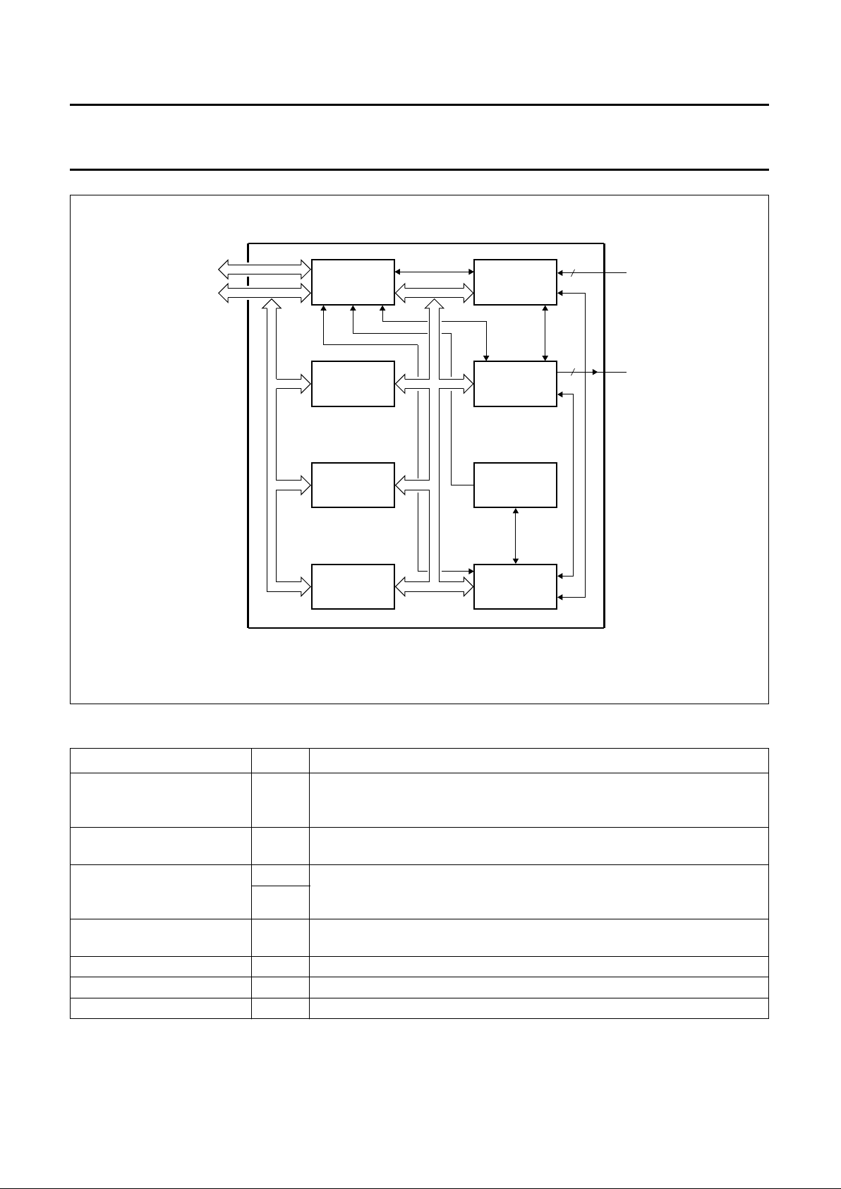
13.3 Interface between CPU and CAN
The internal interface between the P8xC592's CPU and
on-chip CAN-controller is achieved via the following four
SFRs (see Fig.13):
• CANADR, to point to a register of the CAN-controller
• CANDAT, to read or write data
• CANCON, to read interrupt flags and to write commands
• CANSTA, to read status information and to write DMA
pointer.
Additionally, the DMA-logic allows a high-speed data
exchange between the CAN-controller and the CPU's
on-chip MAIN RAM. For more information, see
Section 13.5.15 “Handling of the CPU-CAN interface”.
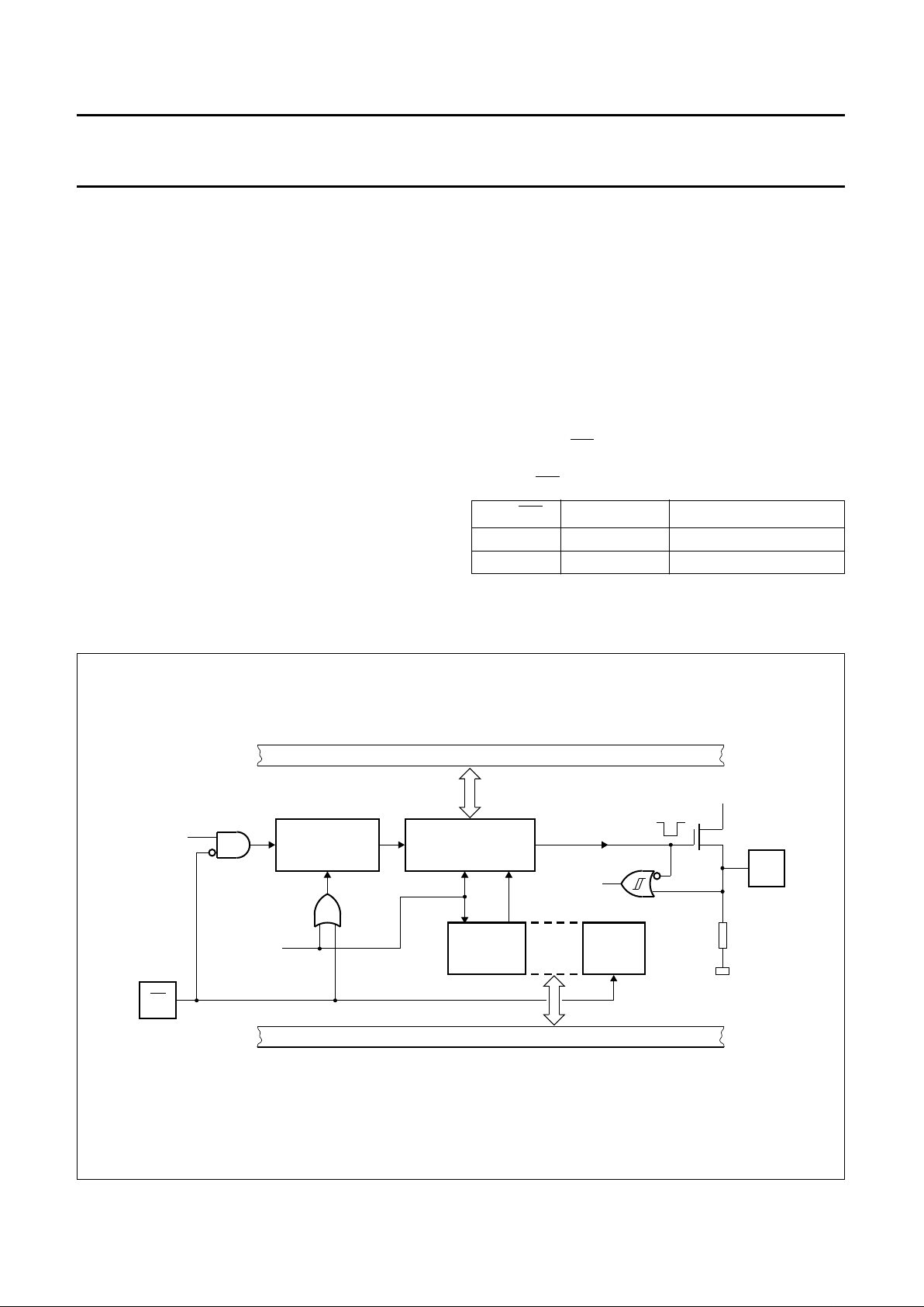
13.4 Hardware blocks of the CAN-controller
The P8xC592 CAN-controller contains all necessary
hardware for high performance serial network
communications (see Fig.14 and Table 29).
It controls the communication flow through the area
network using the CAN-protocol. The CAN-controller
meets the following automotive requirements:
• Short message length
• Bus access priority, determined by the message
identifier
• Powerful error handling capability
• Configuration flexibility to allow area network expansion
• Guaranteed latency time for urgent messages;
– The latency time defines the period between the
initiation (Transmission Request) and the start of the
transmission on the bus. The latency time strongly
depends on a large variety of bus-related conditions.
In the case of a message being transmitted on the
bus and one distortion, the latency time can be up to
149 bit times (worst case). For more information see
Chapter 22 “CAN application information”.
handbook, full pagewidth
CANADR
DBH
CANDAT
DAH
CANCON
D9H
CANSTA
D8H
ADDRESS
DATA
CAN
CONTROLLER
MAIN
RAM
CPU
DMA
LOGIC
internal
bus
4 special function
registers
MGA158
DMA bus
Fig.13 Interface between CPU and CAN-controller.
1996 Jun 27 29
Philips Semiconductors Product specification
8-bit microcontroller with on-chip CAN P8xC592
Table 29 Hardware blocks of the CAN-controller (see Fig.14)
NAME BLOCK DESCRIPTION
Interface Management Logic IML Interprets commands from the CPU, allocates the message buffers
(TBF, RBF0 and RBF1) and provides interrupts and status information to the
microcontroller.
Transmit Buffer TBF 10 bytes memory into which the CPU writes messages which are to be
transmitted over the CAN network.
Receive Buffers (0 and 1) RBF0 RBF0 and RBF1 are each 10 bytes memories which are alternatively used to
store messages received from the CAN network.
The CPU can process one message while another is being received.
RBF1
Bit Stream Processor BSP Is a sequencer, controlling the data stream between the Transmit Buffer,
Receive Buffers (parallel data) and the CAN-bus (serial data).
Bit Timing Logic BTL Synchronizes the CAN-controller to the bitstream on the CAN-bus.
Transceiver Control Logic TCL Controls the output driver.
Error Management Logic EML Performs the error confinement according to the CAN-protocol.
Fig.14 Block diagram of the P8xC592 on-chip CAN-controller.
handbook, full pagewidth
MGA159
INTERFACE
MANAGEMENT
LOGIC
TRANSCEIVER
LOGIC
TRANSMIT
BUFFER
BIT TIMING
LOGIC
2
2
ON - CHIP
CAN
CONTROLLER
RECEIVE
BUFFER 0
RECEIVE
BUFFER 1
BIT STREAM
PROCESSOR
ERROR
MANAGEMENT
LOGIC
address
data
CRX0
and
CRX1
CTX0
and
CTX1
1996 Jun 27 30
Philips Semiconductors Product specification
8-bit microcontroller with on-chip CAN P8xC592
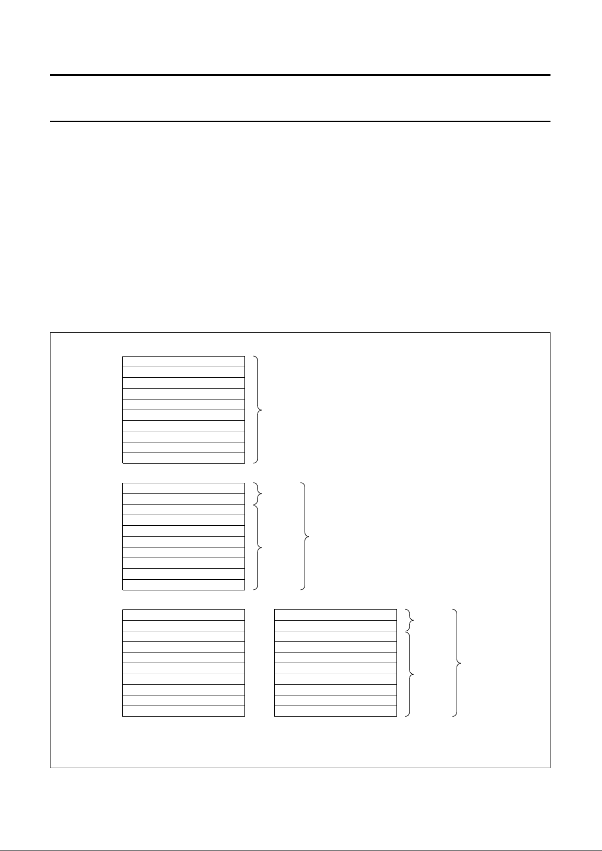
13.5 Control Segment and Message Buffer
description
The CAN-controller appears to the CPU as a
memory-mapped peripheral, guaranteeing the
independent operation of both parts.
13.5.1 A
DDRESS ALLOCATION
The address area of the CAN-controller consists of the
Control Segment and the message buffers. The Control
Segment is programmed during an initialization down-load
in order to configure communication parameters (e.g. bit
timing). The communication over the CAN-bus is also
controlled via this segment by the CPU. A message which
is to be transmitted, must be written to the Transmit Buffer.
After a successful reception the CPU may read the
message from the Receive Buffer and then release it for
further use.
13.5.2 CONTROL SEGMENT LAYOUT
The exchange of status, control and command signals
between the CPU and the CAN-controller is performed in
the control segment. The layout of this segment is shown
in Fig.15. After an initial down-load, the contents of the
registers Acceptance Code, Acceptance Mask,
Bus Timing 0, Bus Timing 1 and Output Control should not
be changed. These registers may only be accessed when
the Reset Request bit in the Control Register is set HIGH
(see Tables 30, 31 and 32).
handbook, full pagewidth
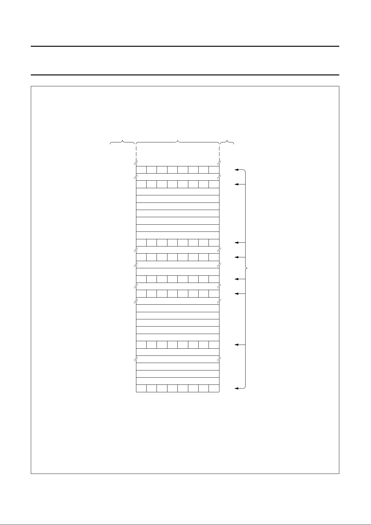
ADDRESS
0
control segment
MGA160 - 1
CONTROL
descriptor
data field
transmit buffer
descriptor
data field
receive buffer 0 or 1
1 COMMAND
2 STATUS
3 INTERRUPT
4 ACCEPTANCE CODE
5 ACCEPTANCE MASK
6 BUS TIMING 0
7 BUS TIMING 1
8 OUTPUT CONTROL
9 TEST
10 IDENTIFIER,
11 RTR BIT, DATA LENGTH CODE
12 BYTE 1
13 BYTE 2
14 BYTE 3
15 BYTE 4
16 BYTE 5
17 BYTE 6
18 BYTE 7
19 BYTE 8
2014H
15H
16H
11H
12H
13H
17H
18H
19H
1AH
1BH
1CH
1DH
IDENTIFIER,
21 RTR BIT, DATA LENGTH CODE
22 BYTE 1
23 BYTE 2
24 BYTE 3
25 BYTE 4
26 BYTE 5
27 BYTE 6
28 BYTE 7
29 BYTE 8
IDENTIFIER,
RTR BIT, DATA LENGTH CODE
BYTE 1
BYTE 2
BYTE 3
BYTE 4
BYTE 5
BYTE 6
BYTE 7
BYTE 8
00H
01H
02H
03H
04H
05H
06H
07H
08H
09H
0AH
0CH
0DH
0EH
0FH
10H
0BH
Fig.15 CAN-controller internal address allocation.
 Loading...