

Philips ne5517 DATASHEETS
Philips Semiconductors Linear Products Product specification
NE5517/5517ADual operational transconductance amplifier
92
August 31, 1994 853-0887 13721
DESCRIPTION
The NE5517 contains two current-controlled transconductance
amplifiers, each with a differential input and push-pull output. The
NE5517 offers significant design and performance advantages over
similar devices for all types of programmable gain applications.
Circuit performance is enhanced through the use of linearizing
diodes at the inputs which enable a 10dB signal-to-noise
improvement referenced to 0.5% THD. The NE5517 is suited for a
wide variety of industrial and consumer applications and is
recommended as the preferred circuit in the Dolby* HX (Headroom
Extension) system.
Constant impedance buffers on the chip allow general use of the
NE5517. These buffers are made of Darlington transistor and a
biasing network which changes bias current in dependence of I
ABC
.
Therefore, changes of output offset voltages are almost eliminated.
This is an advantage of the NE5517 compared to LM13600. With
the LM13600, a burst in the bias current I
ABC
guides to an audible
offset voltage change at the output. With the constant impedance
buffers of the NE5517 this effect can be avoided and makes this
circuit preferable for high quality audio applications.
FEATURES
•Constant impedance buffers
•∆VBE of buffer is constant with amplifier IBIAS change
•Pin compatible with LM13600
•Excellent matching between amplifiers
•Linearizing diodes
•High output signal-to-noise ratio
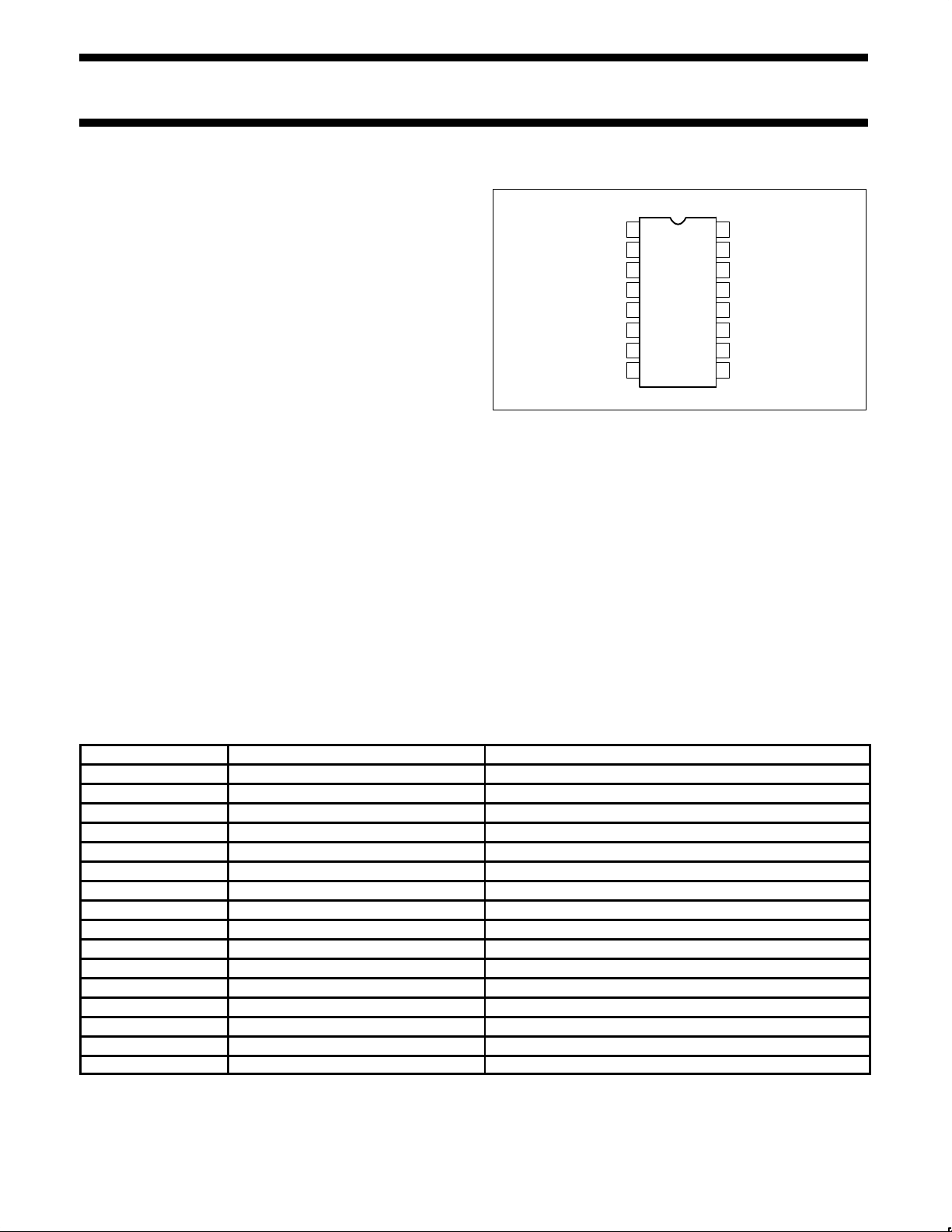
PIN CONFIGURATION
1
2
3
4
5
6
7
8
9
10
11
12
13
14
16
15
I
ABCa
D
a
+IN
a
-IN
a
VO
a
V-
INBUFFER
a
VO
BUFFERa
I
ABCb
D
b
+IN
b
-IN
b
VO
b
V+
IN
BUFFERb
VO
BUFFERb
N, D Packages
Top View
APPLICATIONS
•Multiplexers
•Timers
•Electronic music synthesizers
•Dolby HX Systems
•Current-controlled amplifiers, filters
•Current-controlled oscillators, impedances
Dolby is a registered trademark of Dolby Laboratories Inc., San Francisco, Calif.
PIN DESIGNATION
PIN NO. SYMBOL NAME AND FUNCTION
1 I
ABC
Amplifier bias input A
2 D Diode bias A
3 +IN Non-inverting input A
4 -IN Inverting input A
5 V
O
Output A
6 V- Negative supply
7 IN
BUFFER
Buffer input A
8 VO
BUFFER
Buffer output A
9 VO
BUFFER
Buffer output B
10 IN
BUFFER
Buffer input B
11 V+ Positive supply
12 V
O
Output B
13 -IN Inverting input B
14 +IN Non-inverting input B
15 D Diode bias B
16 I
ABC
Amplifier bias input B
Philips Semiconductors Linear Products Product specification
NE5517/5517ADual operational transconductance amplifier
August 31, 1994
93
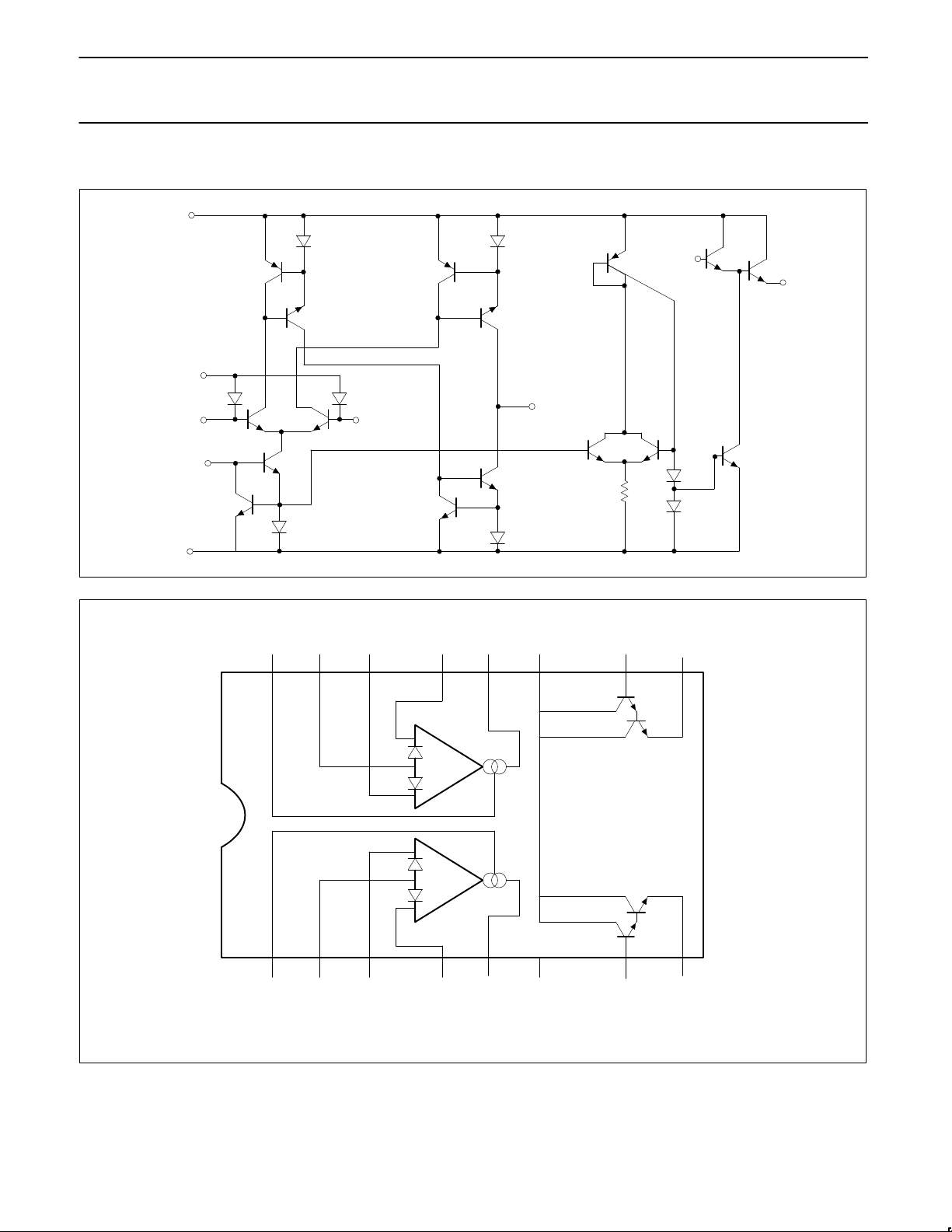
CIRCUIT SCHEMATIC
V+
11
D4
Q6
Q7
2,15
D2
Q4
Q5
D3
–INPUT
4,13
+INPUT
3,14
AMP BIAS
INPUT
1,16
Q2
Q1
D1
V–
6
Q10
D6
Q11
V
OUTPUT
5,12
Q9
Q8
D5
Q14
Q15 Q16
R1
D7
D8
Q3
7,10
Q12
Q13
8,9
CONNECTION DIAGRAM
NOTE:
1. V+ of output buffers and amplifiers are internally connected.
B
AMP
BIAS
INPUT
B
DIODE
BIAS
B
INPUT
(+)
B
INPUT
(–)
B
OUTPUT
V+ (1)
B
BUFFER
INPUT
B
BUFFER
OUTPUT
AMP
BIAS
INPUT
DIODE
BIAS
INPUT
(+)
INPUT
(–)
OUTPUT
V–
BUFFER
INPUT
BUFFER
OUTPUT
A
A A
A
A
A
A
1 2 3 4 5 6 7 8
16 15 14 13 12 11 10 9
–
+
B
+
–
A
Philips Semiconductors Linear Products Product specification
NE5517/5517ADual operational transconductance amplifier
August 31, 1994
94
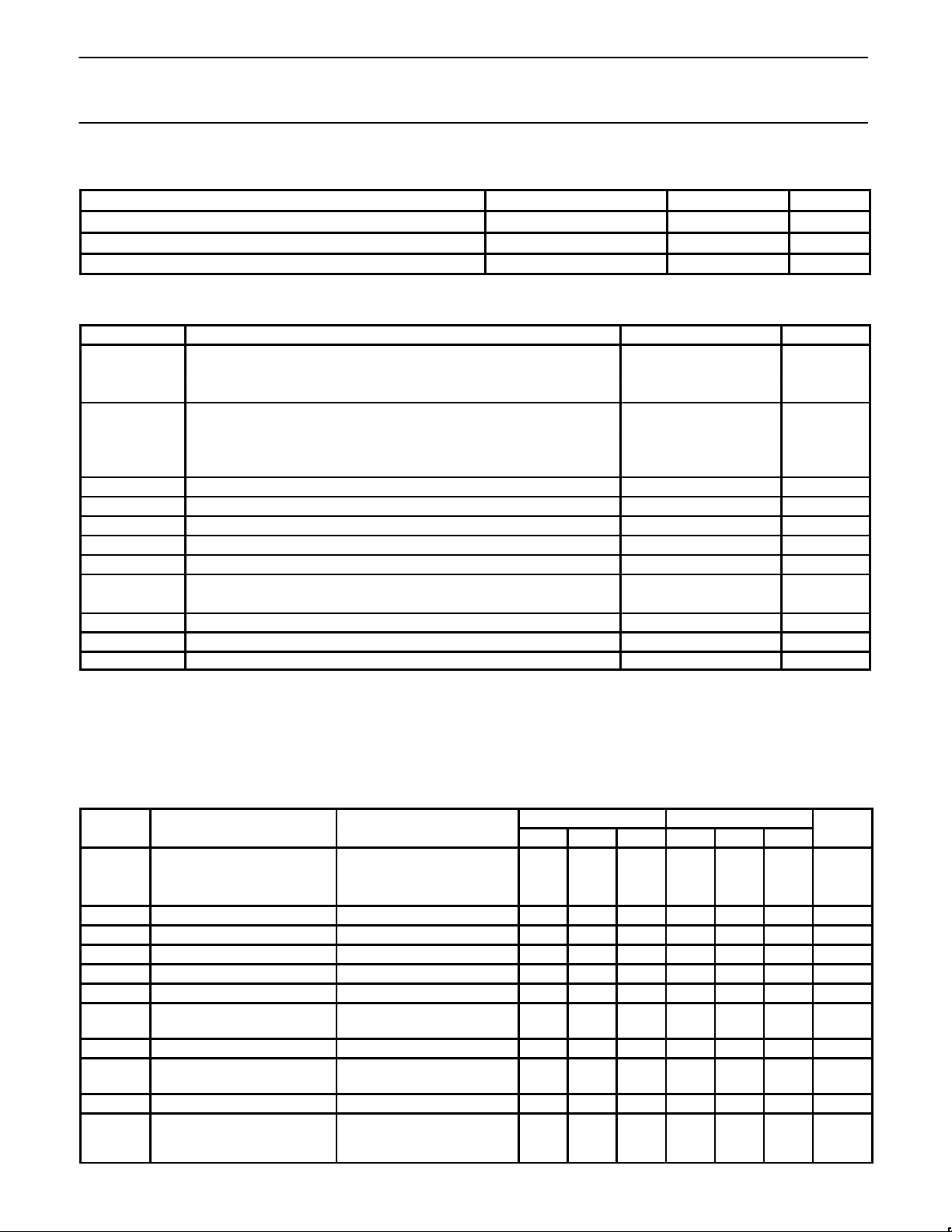
ORDERING INFORMATION
DESCRIPTION TEMPERATURE RANGE ORDER CODE DWG #
16-Pin Plastic Dual In-Line Package (DIP) 0 to +70°C NE5517N 0406C
16-Pin Plastic Dual In-Line Package (DIP) 0 to +70°C NE5517AN 0406C
16-Pin Small Outline (SO) Package 0 to +70°C NE5517D 0005D
ABSOLUTE MAXIMUM RATINGS
SYMBOL PARAMETER RATING UNIT
V
S
Supply voltage
1
NE5517 36 VDC or ±18 V
NE5517A 44 VDC or ±22 V
P
D
Power dissipation,
T
A
=25°C (still air)
2
NE5517N, NE5517AN 1500 mW
NE5517D 1125 mW
V
IN
Differential input voltage ±5 V
I
D
Diode bias current 2 mA
I
ABC
Amplifier bias current 2 mA
I
SC
Output short-circuit duration Indefinite
I
OUT
Buffer output current
3
20 mA
T
A
Operating temperature range
NE5517N, NE5517AN 0°C to +70 °C
V
DC
DC input voltage +VS to -V
S
T
STG
Storage temperature range -65°C to +150°C °C
T
SOLD
Lead soldering temperature (10sec max) 300 °C
NOTES:
1. For selections to a supply voltage above ±22V, contact factory
2. The following derating factors should be applied above 25°C
N package at 12.0mW/°C
D package at 9.0mW/°C
3. Buffer output current should be limited so as to not exceed package dissipation.
DC ELECTRICAL CHARACTERISTICS
1
NE5517 NE5517A
SYMBOL
PARAMETER
TEST CONDITIONS
Min Typ Max Min Typ Max
UNIT
0.4 5 0.4 2 mV
V
OS
Input offset voltage Over temperature range 5 mV
I
ABC
5µA 0.3 5 0.3 2 mV
∆VOS/∆T Avg. TC of input offset voltage 7 7 µV/°C
VOS including diodes Diode bias current (ID)=500µA 0.5 5 0.5 2 mV
V
OS
Input offset change 5µA ≤ I
ABC
≤ 500µA 0.1 0.1 3 mV
I
OS
Input offset current 0.1 0.6 0.1 0.6 µA
∆IOS/∆T Avg. TC of input offset current 0.001 0.001 µA/°C
I
BIAS
Input bias current
Over temperature range
0.4
1
5
8
0.4
1
5
7
µA
µA
∆IB/∆T Avg. TC of input current 0.01 0.01 µA/°C
g
M
Forward transconductance
Over temperature range
6700
5400
9600 13000 7700
4000
9600 12000 µmho
µmho
gM tracking 0.3 0.3 dB
I
OUT
Peak output current
RL=0, I
ABC
=5µA
R
L
=0, I
ABC
=500µA
R
L
=0,
350
300
5
500
650
3
350
300
5
5007650
µA
µA
µA
Philips Semiconductors Linear Products Product specification
NE5517/5517ADual operational transconductance amplifier
August 31, 1994
95
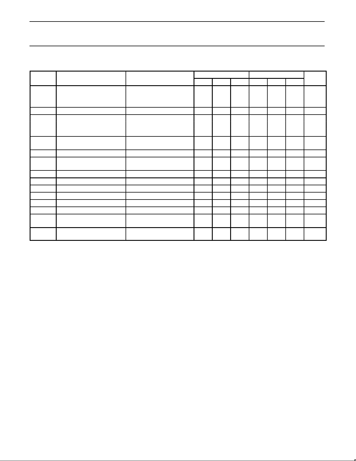
DC ELECTRICAL CHARACTERISTICS1 (continued)
NE5517 NE5517A
SYMBOL
PARAMETER
TEST CONDITIONS
Min Typ Max Min Typ Max
UNIT
V
OUT
Peak output voltage
Positive RL=∞, 5µA≤I
ABC
≤500µA +12 +14.2 +12 +14.2 V
Negative RL=∞, 5µA≤I
ABC
≤500µA -12 -14.4 -12 -14.4 V
I
CC
Supply current I
ABC
=500µA, both channels 2.6 4 2.6 4 mA
VOS sensitivity
Positive ∆ VOS/∆ V+ 20 150 20 150 µV/V
Negative ∆ VOS/∆ V- 20 150 20 150 µV/V
CMRR
Common-mode rejection
ration
80 110 80 110 dB
Common-mode range ±12 ±13.5 ±12 ±13.5 V
Crosstalk
Referred to input2
20Hz<f<20kHz
100 100 dB
I
IN
Differential input current I
ABC
=0, input=±4V 0.02 100 0.02 10 nA
Leakage current I
ABC
=0 (Refer to test circuit) 0.2 100 0.2 5 nA
R
IN
Input resistance 10 26 10 26 kΩ
B
W
Open-loop bandwidth 2 2 MHz
SR Slew rate Unity gain compensated 50 50 V/µs
IN
BUFFER
Buff. input current 5 0.4 5 0.4 5 µA
VO-
BUFFER
Peak buffer output voltage 5 10 10 V
∆VBE of buffer
Refer to Buffer VBE test3
circuit
0.5 5 0.5 5 mV
NOTES:
1. These specifications apply for VS=±15V, TA=25°C, amplifier bias current (I
ABC
)=500µA, Pins 2 and 15 open unless otherwise specified. The
inputs to the buffers are grounded and outputs are open.
2. These specifications apply for V
S
=±15V, I
ABC
=500µA, R
OUT
=5kΩ connected from the buffer output to -VS and the input of the buffer is
connected to the transconductance amplifier output.
3. V
S
=±15, R
OUT
=5kΩ connected from Buffer output to -VS and 5µA ≤I
ABC
≤500µA.
 Loading...