

Page 1
Philips Semiconductors Linear Products Product specification
NE/SE5514Quad high-performance operational amplifier
82
August 31, 1994 853-1175 13721
DESCRIPTION
The NE/SE5514 family of quad operational amplifiers sets new
standards in bipolar quad amplifier performance. The amplifiers
feature low input bias current and low offset voltages. Pinout is
identical to LM324/LM348 which facilitates direct product
substitution for improved system performance in dual supply
applications. Output characteristics are similar to a µA741 with
improved slew and drive capability.
FEATURES
•Low input bias current: < ±3nA
•Low input offset current: < ±3nA
•Low input offset voltage:<1mV
•Low supply current: 1.5mA/A
•1V/µs slew rate
•High input impedance: 100MΩ
•High common-mode impedance: 10GΩ
•Internal compensation for unity gain
•600Ω drive capability (7V
RMS
)
APPLICATIONS
•AC amplifiers
•RC active filters
•Transducer amplifiers
•DC gain block
•Instrumentation amplifier
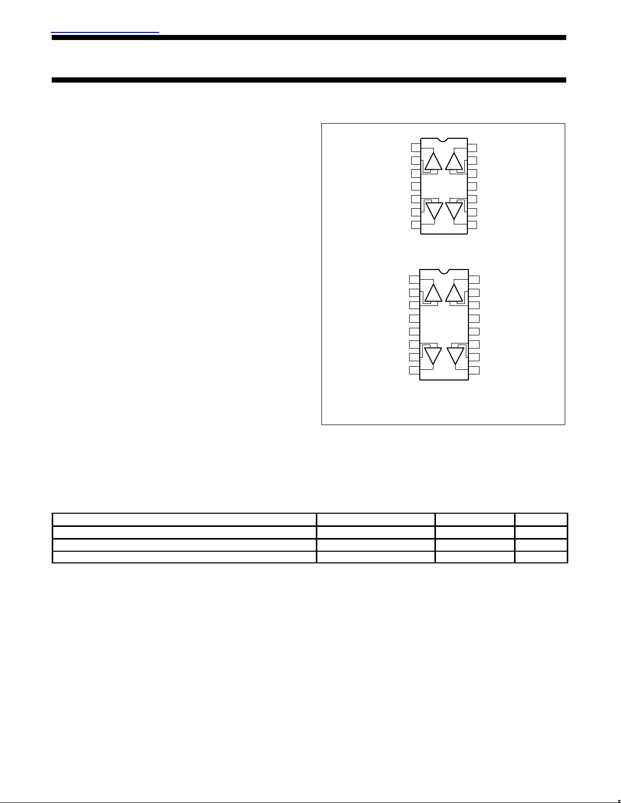
PIN CONFIGURATIONS
N Packages
D Package
1
NOTE:
1. SOL - Released in 16-lead large SO package
only. Pinout is different than N package.
1
2
3
4
5
6
7 8
14
13
12
11
10
9
1
2
3
4
5
6
7
8
9
10
11
12
13
14
16
15
OUTPUT 1
–INPUT 1
V+
+INPUT 2
OUTPUT 2
+INPUT 1
–INPUT 2
OUTPUT 1
–INPUT 1
V–
+INPUT 2
OUTPUT 2
+INPUT 1
–INPUT 2
OUTPUT 1
–INPUT 1
V+
+INPUT 2
OUTPUT 2
+INPUT 1
–INPUT 2
OUTPUT 1
–INPUT 1
V–
+INPUT 2
OUTPUT 2
+INPUT 1
–INPUT 2
NC NC
1
2
3 4
1
2
3 4
ORDERING INFORMATION
DESCRIPTION TEMPERATURE RANGE ORDER CODE DWG #
16-Pin Plastic Small Outline Large (SOL) package 0 to +70°C NE5514D 0171B
14-Pin Plastic Dual In-Line Package (DIP) 0 to +70°C NE5514N 0405B
14-Pin Plastic Dual In-Line Package (DIP) -55 to +125°C SE5514N 0405B
查询NE5514D供应商
Page 2

Philips Semiconductors Linear Products Product specification
NE/SE5514Quad high-performance operational amplifier
August 31, 1994
83
EQUIVALENT SCHEMATIC
–V
IN
+V
IN
(ONE OP AMP)
V+
OUTPUT
–V
ABSOLUTE MAXIMUM RATINGS
SYMBOL PARAMETER RATING UNIT
V
CC
Supply voltage ±16 V
V
DIFF
Differential input voltage 32 V
V
IN
Input voltage 0 to 32 V
Output short to ground Continuous
T
STG
Storage temperature range -65 to +150 °C
T
SOLD
Lead soldering temperature (10sec max) 300 °C
T
A
Operating ambient temperature range
NE5514 0 to 70 °C
SE5514 -55 to +125 °C
P
MAX
Maximum power dissipation
TA=25°C (still-air)
1
N package 1420 mW
D package 1250 mW
NOTES:
1. The following derating factors should be applied above 25°C
N package at 11.4mW/°C
D package at 10.0mW/°C
Page 3

Philips Semiconductors Linear Products Product specification
NE/SE5514Quad high-performance operational amplifier
August 31, 1994
84
ELECTRICAL CHARACTERISTICS
V
CC
= ±15V, T
A
= 25°C unless otherwise specified.
SE5514 NE5514
SYMBOL
PARAMETER
TEST CONDITIONS
Min Typ Max Min Typ Max
UNIT
V
OS
Input offset voltage
RS=100Ω, TA=+25°C
Over temp.
0.7
1
2
3
1
1.5
5
6
mV
∆V
OS
Over temp. 4 5 µV/°C
I
OS
Input offset current
RS=100kΩ, TA=+25°C
Over temp.
3
4
10
20
6
8
20
30
nA
∆I
OS
Over temp. 30 40 pA/°C
I
BIAS
Input bias current
RS=100kΩ, TA=+25°C
Over temp.
3
4
10
20
6
8
20
30
nA
∆I
BIAS
Over temp. 30 40 pA/°C
R
IN
Input resistance differential TA=25°C 100 100 MΩ
V
CM
Input common mode range
TA=25°C
Over temp.
±13.5
±13
±13.7
±13.2
±13.5
±13
±13.7
±13.2
V
VCC=±15V,
CMRR
Input common-mode rejection
ratio
VIN=±13.5V @ TA=25°C 70 100 70 100 dB
VIN=±13V @ Over temp.
A
V
Large-signal voltage gain
RL=2kΩ, TA=25°C
V
O
= ±10V, Over temp.
5025200 5025200
V/mV
SR Slew rate TA=25°C 0.6 1 0.6 1 V/µs
GBW
Small-signal unity gain bandwidth
TA=25°C 3 3 MHz
θ
M
Phase margin TA=25°C 45 45 Deg
V
OUT
Output voltage swing
RL=2kΩ, TA=25°C
Over temp.
±13
±12.5
±13.5
±13
±13
±12.5
±13.5
±13
V
V
OUT
Output voltage swing
RL=600Ω1, TA=25°C
Over temp.
±10
±7.5
±11.5
± 9
±10
± 8
±11.5
± 9
V
I
CC
Power supply current
RL=Open, TA=25°C
Over temp.
6
7
10
12
6
7
10
12
mA
PSRR Power supply rejection ratio
±5V ≤ VCC ≤ ±15V
Over temp.
80 110 80 110 dB
AA Amplifier to amplifier coupling f=1kHz to 20kHz, TA=25°C -120 -120 dB
THD Total harmonic distortion
f=10kHz, TA=25°C
V
O
=7V
RMS
0.01 0.01 %
V
NOISE
Input noise voltage f=1kHz, TA=25°C 30 30 nV/√Hz
I
SC
Short-circuit current TA=25°C 10 40 60 10 40 60 mA
NOTES:
1. Not to exceed maximum power dissipation.
Page 4

Copyright © Each Manufacturing Company.
All Datasheets cannot be modified without permission.
This datasheet has been download from :
www.AllDataSheet.com
100% Free DataSheet Search Site.
Free Download.
No Register.
Fast Search System.
www.AllDataSheet.com
 Loading...