

Philips ne5410, se5410 DATASHEETS
Philips Semiconductors Linear Products Product specification
NE/SE541010-Bit high-speed multiplying D/A converter
767
August 31, 1994 853-0945 13721
DESCRIPTION
The NE5410/SE5410 are 10-bit Multiplying Digital-to-Analog
Converters pin- and function-compatible with the industry-standard
MC3410, but with improved performance. These are capable of
high-speed performance, and are used as general-purpose building
blocks in cost effective D/A systems.
The NE/SE5410 provides complete 10-bit accuracy and differential
non-linearity over temperature, and a wide compliance voltage
range. Segmented current sources, in conjunction with an R/2R
DAC, provide the binary weighted currents. The output buffer
amplifier and voltage reference have been omitted to allow greater
speed, lower cost, and maximum user flexibility.
FEATURES
•Pin- and function-compatible with MC3410
•10-bit resolution and accuracy (±0.05%)
•Guaranteed differential non-linearity over temperature
•Wide compliance voltage range—-2.5 to +2.5V
•Fast settling time—250ns typical
•Digital inputs are TTL- and CMOS-compatible
•High-speed multiplying input slew rate—20mA/µs
•Reference amplifier internally-compensated
•Standard supply voltages +5V and -15V
APPLICATIONS
•Successive approximation A/D converters
•High-speed, automatic test equipment
•High-speed modems
•Waveform generators
•CRT displays
•Strip CHART and X-Y plotters
•Programmable power supplies
•Programmable gain and attenuation
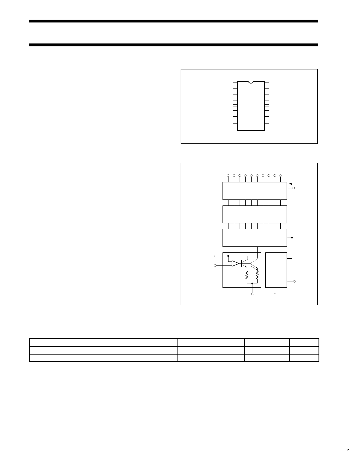
PIN CONFIGURATION
1
2
3
4
5
6
7
8
9
10
11
12
13
14
16
15
F Package
TOP VIEW
V
EE
GND
OUTPUT
D
1
(MSB)
D
2
D
3
D
4
D
5
V
REF
+
D
10
(LSB)
D
9
D
8
D
7
D
6
V
REF
–
V
CC
BLOCK DIAGRAM
MSB LSB
4 5 6 7 8 9 10 11 12 13
3
CURRENT SWITCHES
LADDER TERMINATORS
R-2R LADDER
BIAS
CIRCUITRY
REFERENCE
CURRENT
AMPLIFIER
GND
1 2
14
16
15
D
1D2D3D4D5D6D7D8D9
D
10
V
REF(+)
V
REF(–)
V
CC
I
O
V
EE
ORDERING INFORMATION
DESCRIPTION TEMPERATURE RANGE ORDER CODE DWG #
16-Pin Ceramic Dual In-Line Package (CERDIP) 0 to +70°C NE5410F 0582B
16-Pin Ceramic Dual In-Line Package (CERDIP) -55 to +125°C SE5410F 0582B
Philips Semiconductors Linear Products Product specification
NE/SE541010-Bit high-speed multiplying D/A converter
August 31, 1994
768
ABSOLUTE MAXIMUM RATINGS
TA=+25°C, unless otherwise specified.
SYMBOL
PARAMETER RATING UNIT
V
CC
Power supply +7.0 V
DC
V
EE
-18 V
DC
V
I
Digital input voltage +15 V
DC
V
O
Applied output voltage +4, -5.0 V
DC
I
REF(16)
Reference current 2.5 mA
V
REF
Reference amplifier inputs VCC, V
EE
V
DC
V
REF(D)
Reference amplifier differential inputs 0.7 V
DC
T
A
Operating temperature range
SE5410 -55 to +125 °C
NE5410 0 to +70 °C
T
J
Junction temperature
Ceramic package +150 °C
T
STG
Storage temperature -65 to +150 °C
P
D
Maximum power dissipation
T
A
=25°C (still-air)
1
1190 mW
NOTES:
1. Derate above 25°C at the following rate:
F package at 9.5mW/°C
DC ELECTRICAL CHARACTERISTICS (Continued)
VCC=+5.0VDC, VEE=-15VDC, I
REF
=2.0mA, all digital inputs at high logic level. SE5410: TA=-55°C to +125°C, NE5410 Series: TA=0°C to +70°C,
unless otherwise noted.
LIMITS
SYMBOL
PARAMETER
TEST CONDITIONS
Min Typ Max
UNIT
Relative accuracy Over Temperature ±0.025 ±0.05 %
∈
R
(Error relative to full scale IO) ±1/4 ±1/2 LSB
Differential non-linearity Over temperature ±0.025 ±0.05 %
±1/4 ±1/2 LSB
t
S
Settling time to within ±1/2 LSB
(all bits low to high)
TA = 25°C 250 ns
t
PLH
t
PHL
Propagation delay time TA = 25°C
35
20
ns
TCI
O
Output full-scale current drift 20 40 ppm/°C
V
IH
Digital input logic levels (all bits)
High level, Logic “1”
Low level, Logic “0”
2.0
0.8
V
DC
I
IH
I
IL
Digital input current (all bits)
High level, V
IH
= 5.5V
Low level, V
IL
= 0.8V
20
–20
µA
I
REF(15)
Reference input bias current (Pin 15) –1.0 –5.0 µA
I
OH
Output current (all bits high) V
REF
= 2.000V, R16 = 1000Ω 3.937 3.996 4.054 mA
I
OL
Output currents (all bits low) TA = 25°C 0 0.4 µA
V
O
Output voltage compliance
TA = 25°C
∈
R
< 0.050%
relative to full-scale
–2.5
+2.5
V
DC
SR I
REF
Reference amplifier slew rate 20 mA/µs
ST I
REF
Reference amplifier settling time 0 to 4.0mA, ±0.1% 2.0 µs
PSRR(–) Output current power supply sensitivity 0.003 0.01 %/%
C
O
Output capacitance VO = 0 25 pF

Philips Semiconductors Linear Products Product specification
NE/SE541010-Bit high-speed multiplying D/A converter
August 31, 1994
769
DC ELECTRICAL CHARACTERISTICS
VCC=+5.0VDC, VEE=-15VDC, I
REF
=2.0mA, all digital inputs at high logic level. SE5410: TA=-55°C to +125°C, NE5410 Series: TA=0°C to +70°C,
unless otherwise noted.
LIMITS
SYMBOL
PARAMETER
TEST CONDITIONS
Min Typ Max
UNIT
C
I
Digital input capacitance (all bits high) 4.0 pF
I
CC
I
EE
Power supply current (all bits low)
+2
–12
+4
–18
mA
V
CC
V
EE
Power supply voltage range
TA = 25°C
V
O
= 0
+4.75
–14.25
+5.0
–15
+5.25
–15.75
V
DC
Power consumption 190 300 mW
COMPLIANCE VOLTAGE (VOLT)
Figure 1. Output Current vs Output Compliance Voltage
OUTPUT CURRENT (mA)
4.0
3.0
2.0
1.0
0
–1.0
–5 –3 –1 0 1 3 5
+VCC = +5V
–VEE = –15V
I
REF
= 2mA
TA = 25°C
OUTPUT COMPLIANCE VOLTAGE (VOLTS)
Figure 2. Maximum Output Compliance Voltage
vs Temperature
4.0
3.0
2.0
1.0
0
–1.0
–2.0
–3.0
–4.0
–75 –50 –25 0 25 50 75 100 125
T
A
(°C)
+VCC = +5V
–VEE = –15V
I
REF
= 2mA
CIRCUIT DESCRIPTION
The NE5410 consists of four segment current sources which
generate the 2 Most Significant Bits (MSBs), and an R/2R DAC
implemented with ion-implanted resistors for scaling the remaining 8
Least Significant Bits (LSBs) (see Figure 5). This approach provides
complete 10-bit accuracy without trimming.
The individual bit currents are switched ON or OFF by
fully-differential current switches. The switches use current steering
for speed.
Figure 3. Power Supply Currents vs Temperature
POWER SUPPLY CURRENT (mA)
13
12
11
10
4
3
2
1
0
–75 –50 –25 0 25 50 75 100 125
T
A
(°C)
+VCC = +5V
–VEE = –15V
I
REF
= 2mA
I
EE
+I
CC
II
CC EE
Figure 4. Reference Amplifier Frequency Response
An on-chip high slew reference current amplifier drives the R/2R
ladder and segment decoder. The currents are scaled in such a way
that, with all bits on, the maximum output current is two times
1023/1024 of the reference amplifier current, or nominally 3.996mA
for a 2.000mA reference input current. The reference amplifier
allows the user to provide a voltage input: out-board resistor R16
(see Figure 6) converts this voltage to a usable current. A current
mirror doubles this reference current and feeds it to the segment
decoder and resistor ladder. Thus, for a reference voltage of 2.0V
and a 1kΩ resistor tied to Pin 16, the full-scale current is
 Loading...