

Philips NE5230N, NE5230D, SA5230D, SA5230FE, SA5230N Datasheet

INTEGRATED CIRCUITS
NE/SA5230
Low voltage operational amplifier
Product specification 1994 Aug 31
Philips Semiconductors Product specification
NE/SA5230Low voltage operational amplifier
DESCRIPTION
The NE5230 is a very low voltage operational amplifier that can
perform with a voltage supply as low as 1.8V or as high as 15V. In
addition, split or single supplies can be used, and the output will
swing to ground when applying the latter. There is a bias adjusting
pin which controls the supply current required by the device and
thereby controls its power consumption. If the part is operated at
±0.9V supply voltages, the current required is only 110µA when the
current control pin is left open. Even with this low power
consumption, the device obtains a typical unity gain bandwidth of
180kHz. When the bias adjusting pin is connected to the negative
supply, the unity gain bandwidth is typically 600kHz while the supply
current is increased to 600µA. In this mode, the part will supply full
power output beyond the audio range.
The NE5230 also has a unique input stage that allows the
common-mode input range to go above the positive and below the
negative supply voltages by 250mV . This provides for the largest
possible input voltages for low voltage applications. The part is also
internally-compensated to reduce external component count.
The NE5230 has a low input bias current of typically ±40nA, and a
large open-loop gain of 125dB. These two specifications are
beneficial when using the device in transducer applications. The
large open-loop gain gives very accurate signal processing because
of the large “excess” loop gain in a closed-loop system.
The output stage is a class AB type that can swing to within 100mV
of the supply voltages for the largest dynamic range that is needed
in many applications. The NE5230 is ideal for portable audio
equipment and remote transducers because of its low power
consumption, unity gain bandwidth, and 30nV/√Hz
specification.
noise
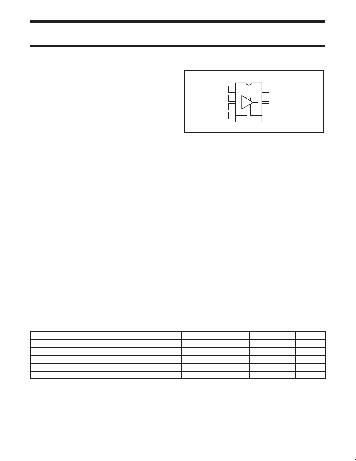
PIN CONFIGURATION
N, D, FE Packages
1
NC
2
–IN
+IN
V
EE
Figure 1. Pin Configuration
–
+
3
45
8
7
6
NC
V
CC
OUTPUT
BIAS ADJ.
SP00250
APPLICATIONS
•Portable precision instruments
•Remote transducer amplifier
•Portable audio equipment
•Rail-to-rail comparators
•Half-wave rectification without diodes
•Remote temperature transducer with 4 to 20mA output
transmission
FEATURES
•Works down to 1.8V supply voltages
•Adjustable supply current
•Low noise
•Common-mode includes both rails
•V
within 100mV of both rails
OUT
ORDERING INFORMATION
DESCRIPTION TEMPERATURE RANGE ORDER CODE DWG #
8-Pin Plastic Small Outline (SO) Package 0 to +70°C NE5230D SOT96-1
8-Pin Plastic Dual In-Line Package (DIP) 0 to +70°C NE5230N SOT97-1
8-Pin Plastic Small Outline (SO) Package -40°C to +85°C SA5230D SOT96-1
8-Pin Ceramic Dual In-Line Package (CERDIP) -40°C to +85°C SA5230FE 0580A
8-Pin Plastic Dual In-Line Package (DIP) -40°C to +85°C SA5230N SOT97-1
1994 Aug 31 853-0942 13721
2
Philips Semiconductors Product specification
NE/SA5230Low voltage operational amplifier
ABSOLUTE MAXIMUM RATINGS
SYMBOL PARAMETER RATING UNIT
V
CC
V
S
V
IN
V
CM
V
CM
P
D
T
J
T
STG
T
SOLD
NOTES:
1. Can exceed the supply voltages when V
2. The maximum operating junction temperature is 150°C. At elevated temperatures, devices must be derated according to the package thermal resistance and device mounting conditions. Derate above 25°C at the following rates:
FE package at 6.7mW/°C
N package at 9.5mW/°C
D package at 6.25mW/°C
3. Momentary shorts to either supply are permitted in accordance to transient thermal impedance limitations determined by the package and
device mounting conditions.
Single supply voltage 18 V
Dual supply voltage ±9 V
Input voltage
Differential input voltage
1
1
±9 (18) V
±V
S
Common-mode voltage (positive) VCC+0.5 V
Common-mode voltage (negative) VEE-0.5 V
Power dissipation
Operating junction temperature
80Output short-circuit duration to either power supply pin
2
2
2, 3
500 mW
150 °C
Indefinite s
Storage temperature -65 to 150 °C
Lead soldering temperature (10sec max) 300 °C
≤±7.5V (15V).
S
V
RECOMMENDED OPERATING CONDITIONS
PARAMETER RATING UNIT
Single supply voltage 1.8 to 15 V
Dual supply voltage ±0.9 to ±7.5 V
Common-mode voltage (positive) VCC+0.25 V
Common-mode voltage (negative) VEE-0.25 V
Temperature
NE grade 0 to 70 °C
SA grade -40 to 85 °C
1994 Aug 31
3

Philips Semiconductors Product specification
SYMBOL
PARAMETER
TEST CONDITIONS
BIAS
UNIT
VOSOffset voltage
mV
IOSOffset current
nA
IOSDrift
nA/°C
IBBias current
nA
IBDrift
nA/°C
V
9V
A
ISSupply current
V
5V
A
VCMCommon-mode input range
V
j
S
PSRR
Power supply rejection ratio
dB
ILLoad current
mA
A
Large-signal open-loop gain
V
5V
NE/SA5230Low voltage operational amplifier
DC AND AC ELECTRICAL CHARACTERISTICS
Unless otherwise specified, ±0.9V ≤ V
temperature range.
V
OS
Drift Any 2 5 µV/°C
pp
CMRR Common-mode rejection ratio VS=±7.5V
pp
VOL
p
≤ +7.5V or equivalent single supply, RL=10kΩ, full input common-mode range, over full operating
S
NE/SA5230
Min Typ Max
TA=25°C Any 0.4 3
TA=25°C Any 3 4
TA=25°C High 3 50
TA=25°C Low 3 30
High 100
Low 60
High 0.5 1.4
Low 0.3 1.4
TA=25°C High 40 150
TA=25°C Low 20 60
High 200
Low 150
High 2 4
Low 2 4
TA=25°C Low 110 160
S
=±0.
TA=25°C High 600 750
Low 250
High 800
TA=25°C Low 320 550
S
=±7.
TA=25°C High 1.1 1.6
Low 600
High 1.7
p
VOS≤6mV, TA=25°C Any V–-0.25 V++0.25
–
RS=10kΩ, VCM=±7.5V,
T
=25°C
A
Any V
Any 85 95
RS=10kΩ, VCM=±7.5V Any 80
TA=25°C High 90 105
TA=25°C Low 85 95
High 75
Low 80
source VS=±7.5V Any 4 10
sink VS=±7.5V Any 5 15
source VS=±7.5V Any 1 5
sink VS=±7.5V Any 2 6
source VS=±0.9V, TA=25°C High 4 6
sink VS=±0.9V, TA=25°C High 5 7
source VS=±7.5V, TA=25°C High 16
sink VS=±7.5V, TA=25°C High 32
RL=10kΩ, TA=25°C High 120 2000 V/mV
p
S
=±7.
RL=10kΩ, TA=25°C Low 60 750
High 100 V/mV
Low 50
°
°
µ
µ
+
V
dB
1994 Aug 31
4
Philips Semiconductors Product specification
SYMBOL
PARAMETER
TEST CONDITIONS
BIAS
UNIT
V
9V
mV
V
Output voltage swing
V
SR
Slew rate
V/µs
BW
Inverting unity gain bandwidth
MH
tSSettling time
s
V
Input noise
nV/√H
THD
Total Harmonic Distortion
%
NE/SA5230Low voltage operational amplifier
DC AND AC ELECTRICAL CHARACTERISTICS (Continued)
NE/SA5230
Min Typ Max
TA=25°C +SW Any 750 800
TA=25°C -SW Any 750 800
+SW Any 700
-SW Any 700
TA=25°C +SW Any 7.30 7.35
+SW Any 7.25 7.30
-SW Any -7.30 -7.35
TA=25°C High 0.25
TA=25°C Low 0.09
RS=0Ω, f=1kHz High 30
RS=0Ω, f=1kHz Low 60
VS=±7.5V
VS=±0.9V
High 0.003
High 0.002
z
µ
z
θ
OUT
M
INN
=±0.
S
p
VS=±7.5V TA=25°C -SW Any -7.32 -7.35
CL=100pF, TA=25°C High 0.6
CL=100pF, TA=25°C Low 0.25
Phase margin CL=100pF, TA=25°C Any 70 Deg.
CL=100pF, 0.1% High 2
CL=100pF, 0.1% Low 5
p
A
=1, VIN=500mV, f=1kHz
V
A
=1, VIN=500mV, f=1kHz
V
1994 Aug 31
5
Philips Semiconductors Product specification
NE/SA5230Low voltage operational amplifier
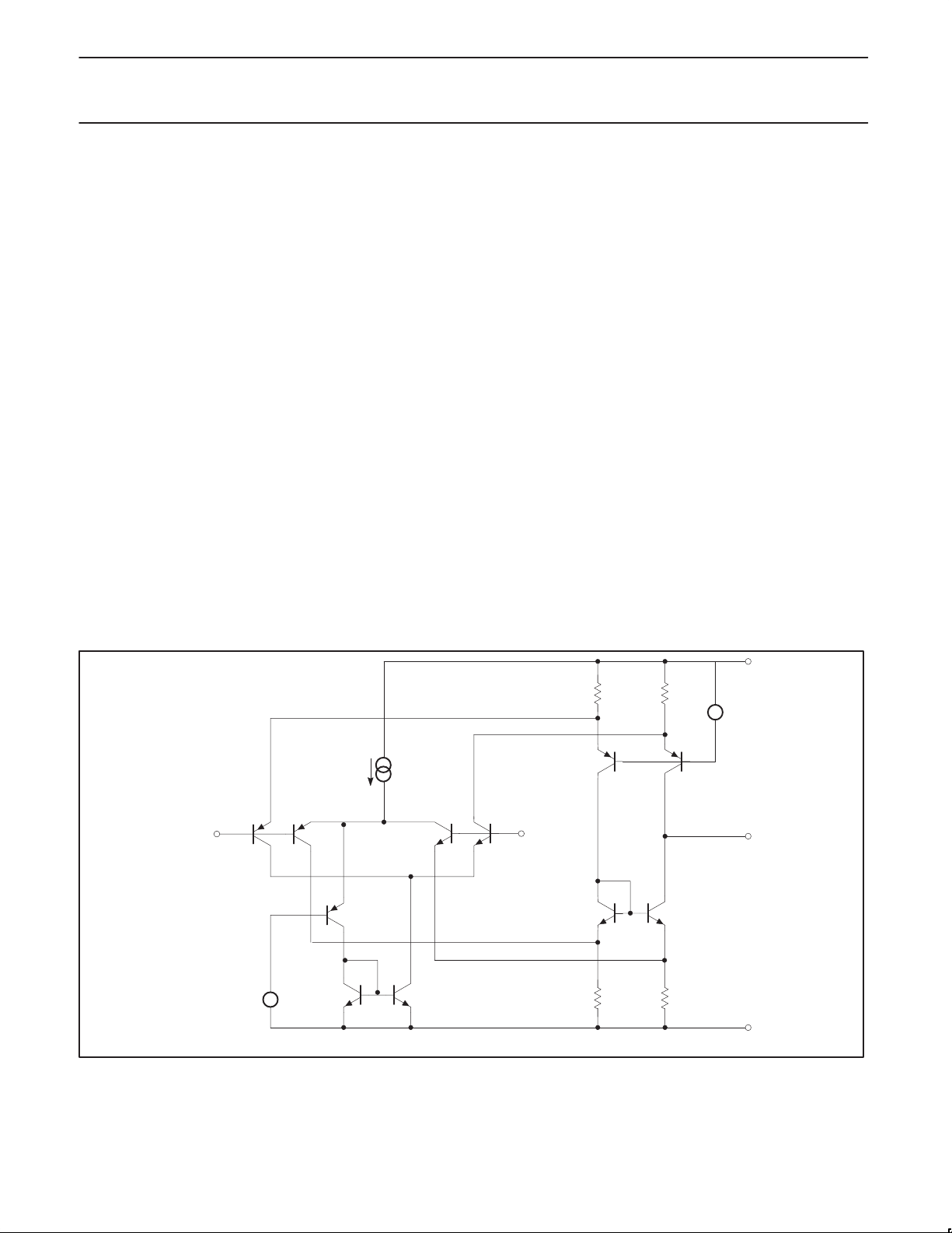
THEORY OF OPERATION
Input Stage
Operational amplifiers which are able to function at minimum supply
voltages should have input and output stage swings capable of
reaching both supply voltages within a few millivolts in order to
achieve ease of quiescent biasing and to have maximum
input/output signal handling capability. The input stage of the
NE5230 has a common-mode voltage range that not only includes
the entire supply voltage range, but also allows either supply to be
exceeded by 250mV without increasing the input offset voltage by
more than 6mV . This is unequalled by any other operational
amplifier today.
In order to accomplish the feat of rail-to-rail input common-mode
range, two emitter-coupled differential pairs are placed in parallel so
that the common-mode voltage of one can reach the positive supply
rail and the other can reach the negative supply rail. The simplified
schematic of Figure 2 shows how the complementary
emitter-coupler transistors are configured to form the basic input
stage cell. Common-mode input signal voltages in the range from
0.8V above V
and Q4, while common-mode input signal voltages in the range of
V
to 0.8V above VEE are processed only by the PNP pair, Q1 and
EE
Q2. The intermediate range of input voltages requires that both the
NPN and PNP pairs are operating. The collector currents of the
input transistors are summed by the current combiner circuit
composed of transistors Q8 through Q11 into one output current.
Transistor Q8 is connected as a diode to ensure that the outputs of
Q2 and Q4 are properly subtracted from those of Q1 and Q3.
to VCC are handled completely by the NPN pair, Q3
EE
The input stage was designed to overcome two important problems
for rail-to-rail capability . As the common-mode voltage moves from
the range where only the NPN pair was operating to where both of
the input pairs were operating, the effective transconductance would
change by a factor of two. Frequency compensation for the ranges
where one input pair was operating would, of course, not be optimal
for the range where both pairs were operating. Secondly, fast
changes in the common-mode voltage would abruptly saturate and
restore the emitter current sources, causing transient distortion.
These problems were overcome by assuring that only the input
transistor pair which is able to function properly is active. The NPN
pair is normally activated by the current source I
through Q5 and
B1
the current mirror Q6 and Q7, assuming the PNP pair is
non-conducting. When the common-mode input voltage passes
below the reference voltage, V
=0.8V at the base of Q5, the
B1
emitter current is gradually steered toward the PNP pair, away from
the NPN pair. The transfer of the emitter currents between the
complementary input pairs occurs in a voltage range of about
120mV around the reference voltage VB1. In this way the sum of the
emitter currents for each of the NPN and PNP transistor pairs is kept
constant; this ensures that the transconductance of the parallel
combination will be constant, since the transconductance of bipolar
transistors is proportional to their emitter currents.
An essential requirement of this kind of input stage is to minimize
the changes in input offset voltage between that of the NPN and
PNP transistor pair which occurs when the input common-mode
voltage crosses the internal reference voltage, V
layout with a cross-coupled quad for each input pair has yielded a
. Careful circuit
B1
typical input offset voltage of less than 0.3mV and a change in the
input offset voltage of less than 0.1mV.
V
CC
Q11
Q9
R11
V
+
V
b2
SL00251
I
OUT
V
EE
R10
I
b1
Q3
V
IN–
Q1
Q5
+
V
b1
V
Q6
Q7
Q2
Q4
V
IN+
Q10
Q8
R8 R9
Figure 2. Input Stage
1994 Aug 31
6
 Loading...