

Philips N74F676D Datasheet

INTEGRATED CIRCUITS
74F676
16-bit serial/parallel-in, serial-out shift
register (3-State)
Product specification
IC15 Data Handbook
1989 Apr 18
Philips Semiconductors Product specification
74F67616-bit serial/parallel-in, serial-out shift register (3-State)
FEA TURES
•16-bit parallel-to-serial conversion
•16-bit serial-in, serial-out
•Chip select control
•Power supply current 48mA typical
•Shift frequency 110MHz tyical
•Available in 300mil-wide 24-pin Slim DIP package
DESCRIPTION
The 74F676 contains 16 flip-flops with provision for synchronous
parallel or serial entry and serial output. When the mode (M) input is
High, information present on the parallel data (D0–D15) inputs is
entered on the falling edge of the clock pulse (CP
When M is Low, data is shifted out of the most significant bit position
while information present on the serial (SI) input shifts into the least
significant bit position. A High signal on the chip select (CS
prevents both parallel and serial operations.
The 16 bit shift register operates in one of three modes, as indicated
in the shift register Function Table.
Hold: A High signal on the Chip Select (CS
and data is stored in the 16 registers.
Serial load: Data present on the SI pin shifts into the register on the
falling edge of CP
. Data enters the Q0 position and shifts toward
Q15 on successive clocks finally appearing on the SO pin.
Parallel load: Data present on D0–D15 is entered into the register
on the falling edge of CP
. The SO output represents the Q15 register
output.
To prevent false clocking, CP
transition of CS
.
must be Low during a Low-to-High
) input signal.
) input
) input prevents clocking
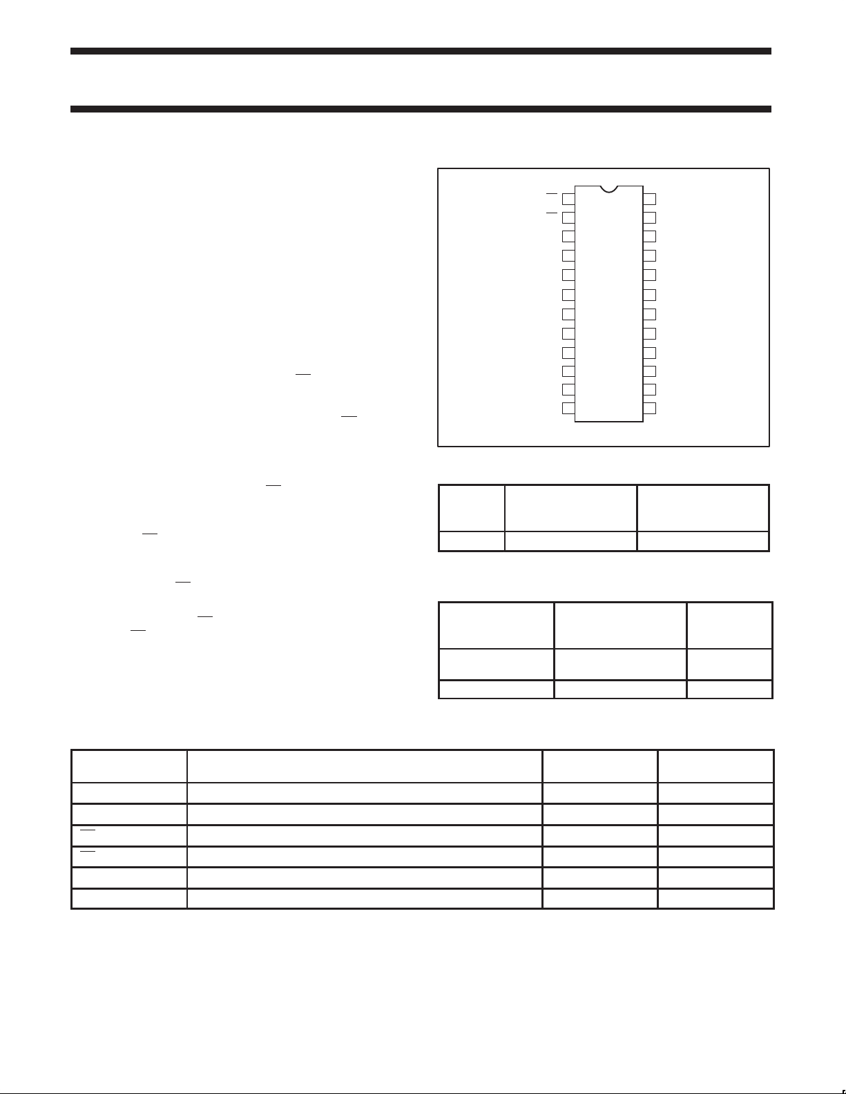
PIN CONFIGURATION
CS
CP
2 D15
3
NC
4
SI
5
M
SO
6
7
D0
D1
8
D2
9
D3
10 15
D4
11
GND
12 13
TYPE TYPICAL f
MAX
74F676 110MHz 48mA
V
241
CC
23
22
D14
21
D13
20
D12
19
D11
18
D10
17
D9
16
D8
D7
14
D6
D5
SF01209
TYPICAL SUPPL Y
CURRENT
(TOTAL)
ORDERING INFORMATION
COMMERCIAL RANGE
DESCRIPTION
24-Pin Plastic Slim
DIP (300mil)
24-Pin Plastic SOL N74F676D SOT137-1
VCC = 5V ±10%,
T
= 0°C to +70°C
amb
N74F676N SOT222-1
PKG DWG #
INPUT AND OUTPUT LOADING AND FAN-OUT TABLE
PINS DESCRIPTION
74F(U.L.)
HIGH/LOW
D0–D15 Parallel data inputs 1.0/1.0 20µA/0.6mA
SI Serial data input 1.0/1.0 20µA/0.6mA
CS Chip Select input (active Low) 1.0/1.0 20µA/0.6mA
CP Clock Pulse input (active falling edge) 1.0/1.0 20µA/0.6mA
M Mode select input 1.0/1.0 20µA/0.6mA
SO Serial data output 50/33 1mA/20mA
NOTE: One (1.0) FAST Unit Load is defined as: 20µA in the High state and 0.6mA in the Low state.
1990 Apr 18 853–0284 99394
2
LOAD VALUE
HIGH/LOW

Philips Semiconductors Product specification
OPERATING MODE
74F67616-bit serial/parallel-in, serial-out shift register (3-State)
LOGIC SYMBOL
4
SI
1
CS
2
CP
5
M
= Pin 24
V
CC
GND = Pin 12
8910
D0 D1 D4 D5 D6 D7D3D2
11 13 147 16 17 18
LOGIC SYMBOL (IEEE/IEC)
SRG16
5
1
2
7
8
9
10
11
13
14
15
16
17
18
19
20
21
22
23
4
0
1
2, 3D
2, 3D
1, 3D
0
M
2
&
C3/1
D8 D9 D12 D13 D14 D15D11D10
SO
6
19 20 21 2215 23
SF01210
6
SF01211
LOGIC DIAGRAM
2
CP
1
CS
5
M
4
SI
7
D0
8
D1
9
D2
10
D3
11
D4
13
D5
14
D6
15
D7
16
D8
17
D9
18
D10
19
D11
CP
Q
D
CP
Q
D
CP
Q
D
CP
Q
D
CP
Q
D
CP
Q
D
CP
Q
D
CP
Q
D
CP
Q
D
CP
Q
D
CP
Q
D
CP
Q
D
FUNCTION TABLE
CONTROL INPUTS
CS M CP
H X X Hold
L L ↓ Shift/Serial load
L H ↓ Parallel load
H = High voltage level
L = Low voltage level
X = Don’t care
↓ = High-to-Low transition of clock input
1990 Apr 18
3
20
D12
21
D13
22
D14
23
D15
VCC = Pin 24
GND = Pin 12
CP
Q
D
CP
Q
D
CP
Q
D
CP
D
6
Q
SO
SF01212
 Loading...