

Philips N74F646D, N74F646N, N74F646AN, N74F648AD, N74F646AD Datasheet
...
INTEGRATED CIRCUITS
74F646, 74F646A
Octal transceiver/register, non-inverting
(3-State)
74F648, 74F648A
Octal transceiver/register, inverting
(3-State)
Product specification
IC15 Data Handbook
1990 Sep 25
Philips Semiconductors Product specification
74F646/A/74F648/AT ransceivers/registers
FEA TURES
•Combines 74F245 and two 74F374 type functions in one chip
•High impedance base inputs for reduced loading (70µA in high
and low states)
•Independent registers for A and B buses
•Multiplexed real-time and stored data
•Choice of non-inverting and inverting data paths
•Controlled ramp outputs for 74F646A/74F648A
•3-state outputs
•300 mil wide 24-pin slim dip package
TYPE
74F646/74F648 115MHz 140mA
74F646A/74F648A 185MHz 105mA
DESCRIPTION
The 74F646/74F646A and 74F648/74F648A transceivers/registers
consist of bus transceiver circuits with 3–state outputs, D–type
flip–flops, and control circuitry arranged for multiplexed transmission
of data directly from the input bus or the internal registers. Data on
the A or B bus will be clocked into the registers as the appropriate
clock pin goes high. Output enable (OE
to control the transceiver function. In the transceiver mode, data
present at the high impedance port may be stored in either the A or
B register or both.
The select (SAB, SBA) pins determine whether data is stored or
transferred through the device in real–time. The DIR determines
which bus will receive data when the OE
isolation mode (OE
register and/or data from bus B may be stored in the A register.
When an output function is disabled, the input function is still
enabled and may be used to store and transmit data. Only one of
the two buses, A or B may be driven at a time.
TYPICAL f
max
= high), data from bus A may be stored in the B
TYPICAL SUPPLY CURRENT ( TOTAL)
) and DIR pins are provided
is active low. In the
ORDERING INFORMATION
ORDER CODE
DESCRIPTION COMMERCIAL RANGE PKG DWG #
VCC = 5V ±10%, T
24–pin plastic slim DIP
(300mil)
24–pin plastic SOL N74F646D, N74F646AD, N74F648D, N74F648AD SOT137-1
N74F646N, N74F646AN, N74F648N, N74F648AN SOT222-1
= 0°C to +70°C
amb
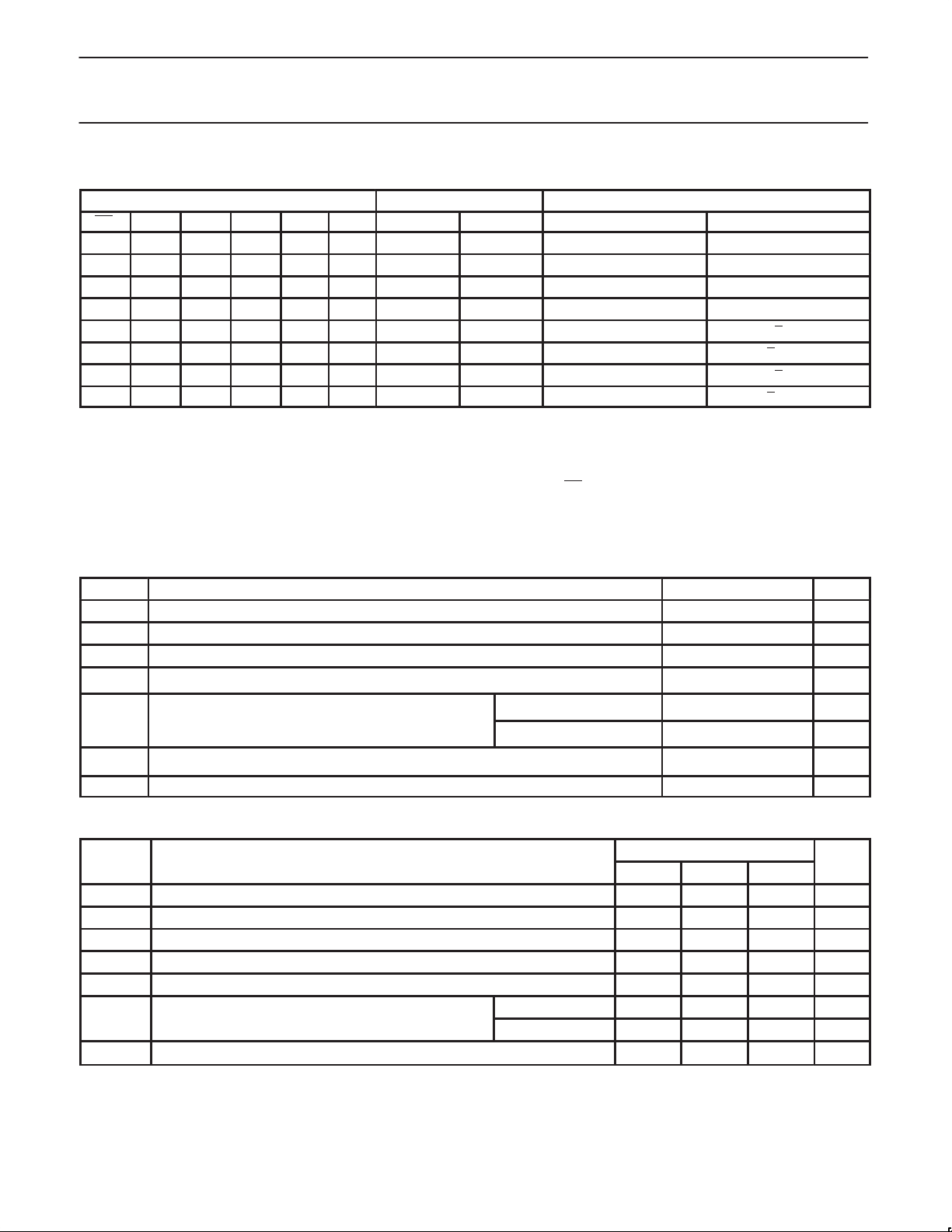
INPUT AND OUTPUT LOADING AND FAN OUT TABLE
PINS DESCRIPTION
A0 – A7, B0 – B7 A and B inputs 3.5/0.1 16 70µA/70µA
CPAB A–to–B clock input 1.0/0.033 20µA/20µA
CPBA B–to–A clock input 1.0/0.033 20µA/20µA
SAB A–to–B select input 1.0/0.033 20µA/20µA
SBA B–to–A select input 1.0/0.033 20µA/20µA
DIR Data flow directional control enable input 1.0/0.033 20µA/20µA
OE Output enable input 1.0/0.033 20µA/20µA
A0 – A7, B0 – B7 A, B outputs for N74F646A/N74F648A 750/80 15mA/48mA
A0 – A7, B0 – B7 A, B outputs for N74F646/N74F648 750/106.7 15mA/64mA
NOTE: One (1.0) FAST unit load is defined as: 20µA in the high state and 0.6mA in the low state.
1990 Sep 25 853-1 124 00515
2
74F (U.L.) HIGH/
LOW
LOAD VALUE HIGH/
LOW
Philips Semiconductors Product specification
74F646/A/74F648/ATransceivers/registers
PIN CONFIGURATION
1
CPAB
2
SAB
3
DIR
4
A0
5
A1
6
A2
7
A3
8
A4
9
A5
10
A6
11
A7
GND
LOGIC SYMBOL
4567891011
A0 A1 A2 A3 A4 A5 A6 A7
CPAB
1
SAB
2
DIR
3
CPBA
23
SBA
22
OE
21
B0 B1 B2 B3 B4 B5 B6 B7
74F646/646A
74F646/646A
24
V
CC
23
CPBA
22
SBA
21
OE
20
B0
19
B1
18
B2
17
B3
16
B4
15
B5
14
B6
1312
B7
SF00386
IEC/IEEE SYMBOL
21
3
23
22
1
2
4
5
6
7
8
9
10
11
LOGIC DIAGRAM
21
OE
3
DIR
23
CPBA
22
SBA
1
CPAB
2
SAB
74F646/646A
G3
3 EN1 [BA]
3 EN2 [AB]
C4
G5
C6
G7
1
1
6D
1
/
74F646/646A
5
4D
1
5
7
1
2
7
20
19
18
17
16
15
14
13
SF00388
V
= Pin 24
CC
GND = Pin 12
1990 Sep 25
20 19 18 17 16 15 14 13
SF00387
3
4
A0
VCC = Pin 24
GND = Pin 12
I of 8 channels
1D
C1
to 7 other channels
1D
C1
20
B0
SF00393
Philips Semiconductors Product specification
74F646/A/74F648/ATransceivers/registers
PIN CONFIGURATION
1
CPAB
2
SAB
3
DIR
4
A0
5
A1
6
A2
7
A3
8
A4
9
A5
10
A6
11
A7
GND
LOGIC SYMBOL
4567891011
74F648/648A
74F648/648A
24
V
23
CPBA
22
SBA
21
OE
20
B0
19
B1
18
B2
17
B3
16
B4
15
B5
14
B6
1312
B7
SF00389
CC
IEC/IEEE SYMBOL
21
3
23
22
1
2
4
5
6
7
8
9
10
11
LOGIC DIAGRAM
74F648/648A
G3
3 EN1 [BA]
3 EN2 [AB]
C4
G5
C6
G7
1
1
7
6D
1
7
5
4D
1
5
1
2
20
19
18
17
16
15
14
13
SF00391
VCC = Pin 24
GND = Pin 12
A0 A1 A2 A3 A4 A5 A6 A7
CPAB
1
SAB
2
DIR
3
CPBA
23
SBA
22
OE
21
B0 B1 B2 B3 B4 B5 B6 B7
20 19 18 17 16 15 14 13
SF00390
OE
DIR
CPBA
SBA
CPAB
SAB
A0
1D
C1
74F648/648A
to 7 other channels
1D
C1
20
B0
SF00400
21
3
23
22
1
2
I of 8 channels
4
1990 Sep 25
4
Philips Semiconductors Product specification
74F646/A/74F648/ATransceivers/registers
FUNCTION TABLE
INPUTS DATA I/O OPERATING MODE
OE DIR CPAB CPBA SAB SBA An Bn 74F646/74F646A 74F648/74F648A
X X ↑ X X X Input Unspecified* Store A, B unspecified* Store A, B unspecified*
X X X ↑ X X Unspecified* Input Store B, A unspecified* Store B, A unspecified*
H X ↑ ↑ X X Input Input Store A and B data Store A and B data
H X H or L H or L X X Input Input Isolation, hold storage Isolation, hold storage
L L X X X L Output Input Real time B data to A bus Real time B data to A bus
L L X H or L X H Output Input Stored B data to A bus Stored B data to A bus
L H X X L X Input Output Real time A data to B bus Real time A data to B bus
L H H or L X H X Input Output Stored A data to B bus Stored A data to B bus
NOTES:
1. H = High–voltage level
2. L = Low–voltage level
3. X = Don’t care
4. ↑ = Low–to–high clock transition
5. * = The data output function may be enabled or disabled by various signals at the OE
always enabled, i.e., data at the bus pins will be stored on every low–to–high transition of the clock.
and DIR inputs. Data input functions are
ABSOLUTE MAXIMUM RATINGS
(Operation beyond the limit set forth in this table may impair the useful life of the device. Unless otherwise noted these limits are over the
operating free air temperature range.)
SYMBOL
V
CC
V
IN
I
IN
V
OUT
I
OUT
T
amb
T
stg
Supply voltage –0.5 to +7.0 V
Input voltage –0.5 to +7.0 V
Input current –30 to +5 mA
Voltage applied to output in high output state –0.5 to V
Current applied to output in low output state 74F646A, 74F648A 72 mA
Operating free air temperature range
Storage temperature range –65 to +150
PARAMETER RATING UNIT
CC
74F646, 74F648 128 mA
0 to +70
RECOMMENDED OPERATING CONDITIONS
SYMBOL PARAMETER LIMITS UNIT
MIN NOM MAX
V
V
V
I
I
I
T
CC
IH
IL
Ik
OH
OL
amb
Supply voltage 4.5 5.0 5.5 V
High–level input voltage 2.0 V
Low–level input voltage 0.8 V
Input clamp current –18 mA
High–level output current –15 mA
Low–level output current 74F646A, 74F648A 48 mA
74F646, 74F648 64 mA
Operating free air temperature range 0 +70
V
°C
°C
°C
1990 Sep 25
5
 Loading...