

Philips N74F641N, N74F642D, N74F642N, N74F641D Datasheet
74F641/74F642*
Transceivers
Product specification
Supersedes data of 1989 Nov 27
IC15 Data Handbook
1999 Jan 08
INTEGRATED CIRCUITS
* Discontinued part. Please see the Discontinued Product List.
Philips Semiconductors Product specification
74F641/74F642*Transceivers
74F641 Octal Bus Transceiver with Common Output Enable, Non-Inverting (Open Collector)
74F642 Octal Bus Transceiver with Common Output Enable, Inverting (Open Collector)
2
1999 Jan 08 853–0382 20616
* Discontinued part. Please see the Discontinued Products List.
FEA TURES
•High-impedance NPN base inputs for reduced loading
(20µA in High and Low states)
•Octal bidirectional bus interface
•Common Output Enable for both Transmit and Receive modes
•Open collector outputs sink 64mA
•—74F641, non-inverting
—74F642, inverting
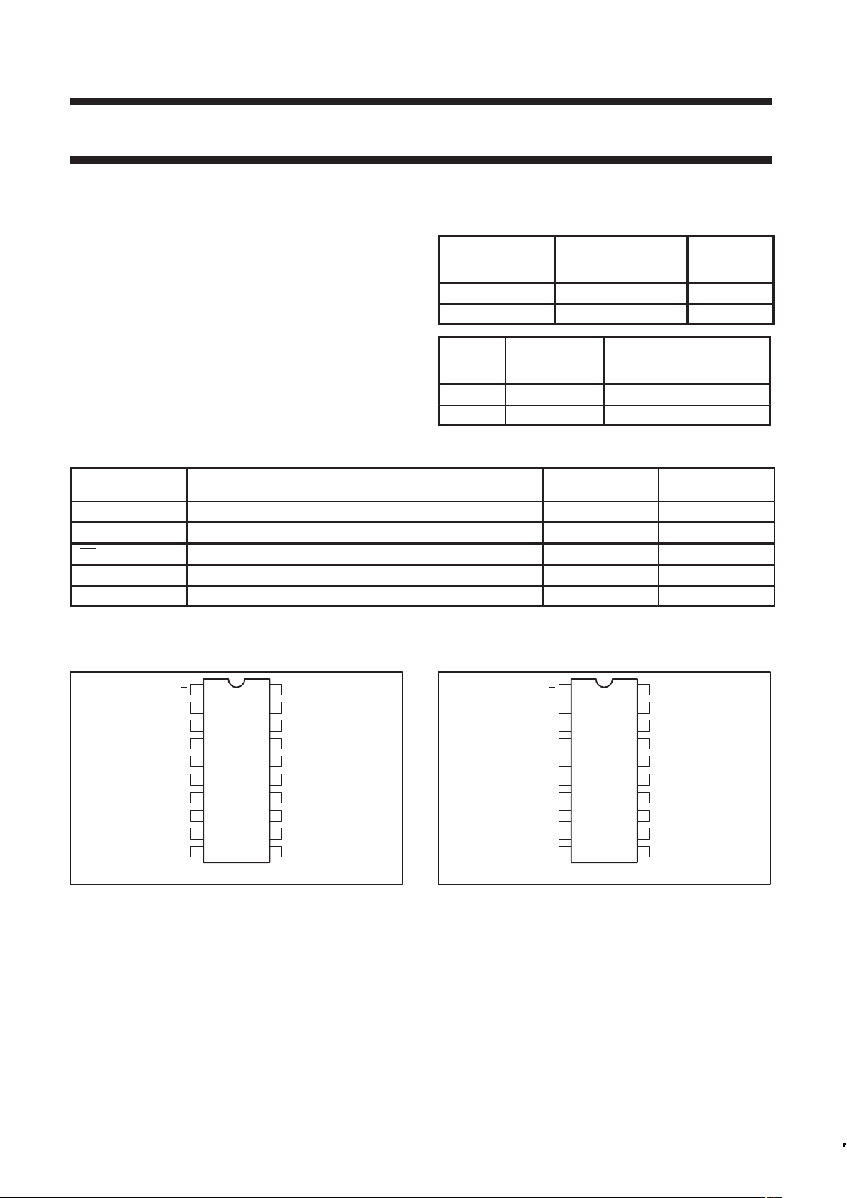
ORDERING INFORMATION
DESCRIPTION
COMMERCIAL RANGE
VCC = 5V ±10%,
T
amb
= 0°C to +70°C
PKG DWG #
20-pin plastic DIP N74F641N SOT146-1
20-pin plastic SOL N74F641D SOT163-1
TYPE
TYPICAL
PROPAGATION
DELA Y
TYPICAL SUPPL Y CURRENT
(TOT AL)
74F641 8.0ns 69mA
74F642 8.5ns 52mA
INPUT AND OUTPUT LOADING AND FAN-OUT TABLE
PINS DESCRIPTION
74F(U.L.)
HIGH/LOW
LOAD VALUE
HIGH/LOW
A0 - A7, B0 - B7 Data inputs 1.0/0.033 20µA/20µA
T/R Transmit/Receive input 2.0/0.067 40µA/40µA
OE Output Enable inputs 2.0/0.067 40µA/40µA
A0 - A7 Data outputs OC/40 OC/24mA
B0 - B7 Data outputs OC/106.7 OC/64mA
NOTE: One (1.0) FAST unit load is defined as: 20µA in the High state and 0.6mA in the Low state. OC = Open Collector.
PIN CONFIGURATION – 74F641
SF00198
1
2
3
4
5
6
7
8
9
10 11
12
13
14
15
16
17
18
19
20
T/R
A0
A1
A2
A3
A4
A5
A6
A7
GND
V
CC
OE
B0
B1
B2
B3
B4
B6
B5
B7
PIN CONFIGURATION – 74F642
SF00198
1
2
3
4
5
6
7
8
9
10 11
12
13
14
15
16
17
18
19
20
T/R
A0
A1
A2
A3
A4
A5
A6
A7
GND
V
CC
OE
B0
B1
B2
B3
B4
B6
B5
B7
Philips Semiconductors Product specification
74F641/74F642*Transceivers
1999 Jan 08
3
* Discontinued part. Please see the Discontinued Products List.
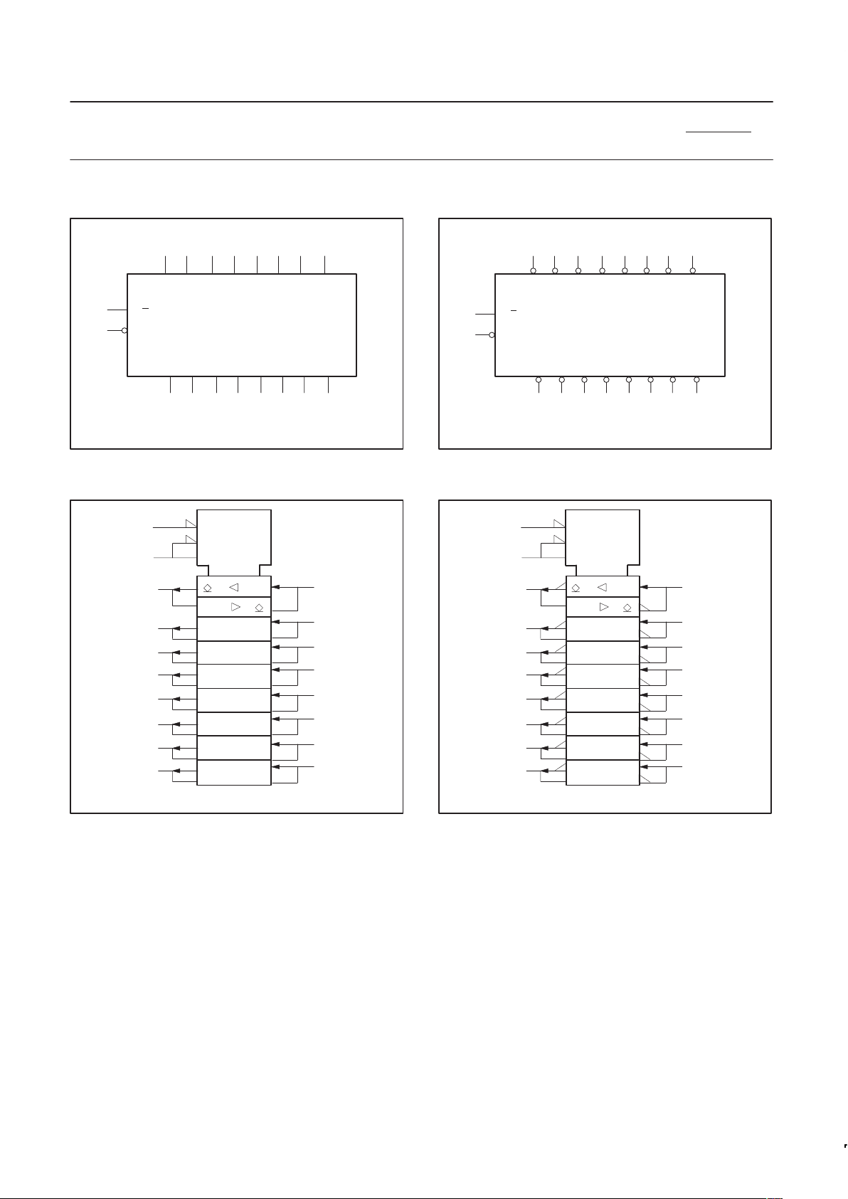
LOGIC SYMBOL – 74F641
B0 B1 B2 B3
19
1
T/R
OE
SF01154
VCC= Pin 20
GND = Pin 10
B4 B5 B6 B7
89
A2 A3
456
A4 A5 A67A7
23
A0 A1
18 17 16 15 14 13 12 11
LOGIC SYMBOL – 74F642
B0 B1 B2 B3
19
1
T/R
OE
SF01146
VCC= Pin 20
GND = Pin 10
B4 B5 B6 B7
89
A2 A3
456
A4 A5 A67A7
23
A0 A1
18 17 16 15 14 13 12 11
LOGIC SYMBOL (IEEE/IEC) – 74F641
SF01147
19
18
G3
3EN1
3EN2
1
17
16
15
14
13
12
11
2
3
4
5
6
7
8
9
2
1
LOGIC SYMBOL (IEEE/IEC) – 74F642
SF01148
19
18
G3
3EN1
3EN2
1
17
16
15
14
13
12
11
2
3
4
5
6
7
8
9
2
1
 Loading...