

INTEGRATED CIRCUITS
74F597
8-bit shift register with input storage
registers
Product specification
IC15 Data Handbook
1991 Sep 13
Philips Semiconductors Product specification
74F5978-bit shift register with input storage registers
FEA TURES
•High impedance PNP base inputs for reduced loading
(20µA in High and Low states)
•8-bit parallel storage register
•3-State output buffers
•Shift register has asynchronous direct overriding reset
•Shift load SHLD is functional when SHCP is Low and locked out
when SHCP is High
•Guaranteed shift frequency DC to 105MHz
DESCRIPTION
The 74F597 consists of an 8-bit storage register feeding a
parallel-in/serial-in, serial-out 8-bit shift register. The storage register
and shift register have separate positive edge triggered clocks. The
shift register has asynchronous reset and when SHCP is Low, it has
asynchronous load.
The shift register load function has been modified to load when both
SHLD
and SHCP are Low. When SHCP is High the shift register
load operation is not performed. Data will be properly shifted on the
rising edge of SHCP when SHLD
is High.
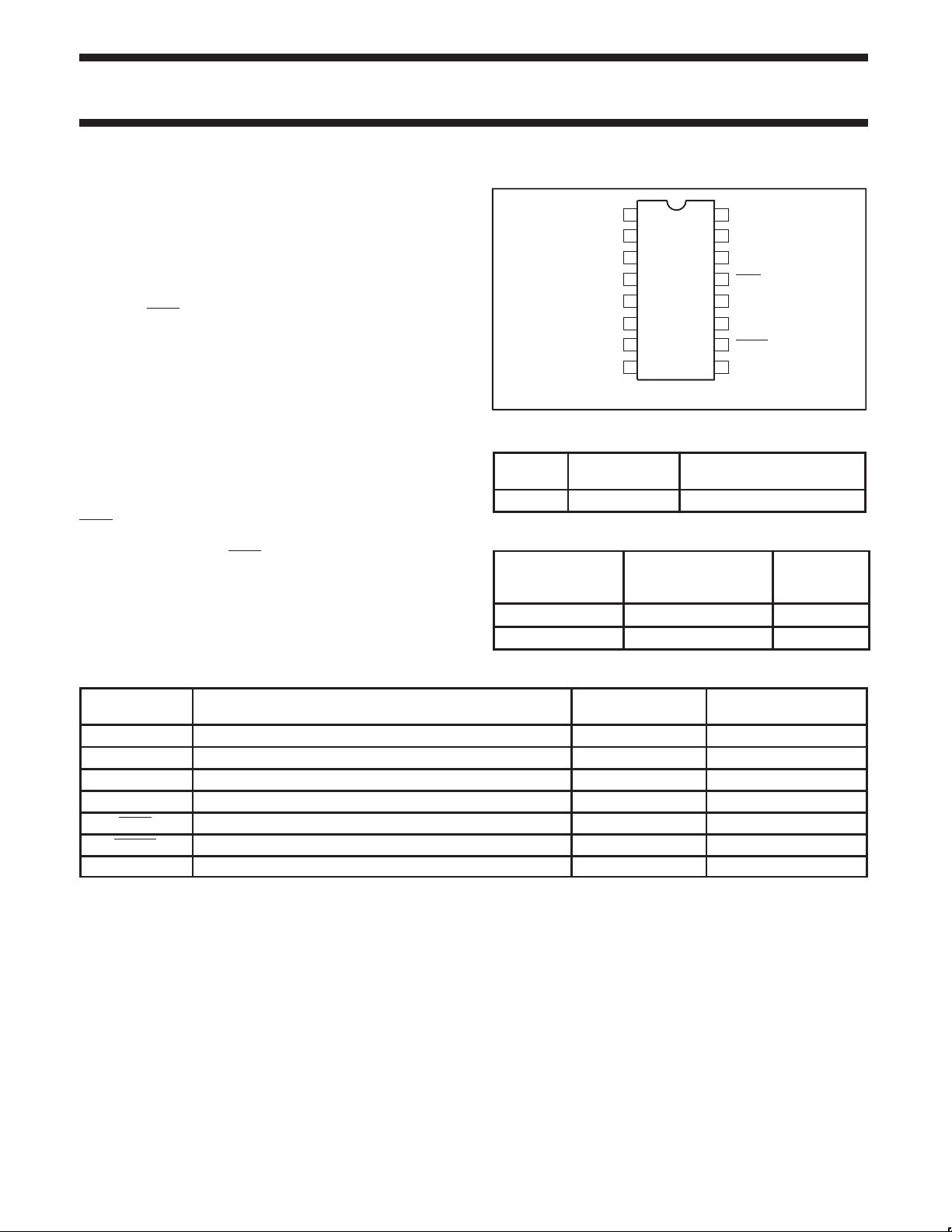
PIN CONFIGURATION
1
D1
2
D2
3
D3
4
D4
5
D5
6
D6
D7
GND
TYPE TYPICAL f
MAX
74F597 135MHz 42mA
16
V
CC
D0
15
D
14
S
SHLD
13
STCP
12
SHCP
11
SHRST
107
98
Q
S
SF00366
TYPICAL SUPPL Y CURRENT
(TOTAL)
ORDERING INFORMATION
COMMERCIAL RANGE
DESCRIPTION
16-pin plastic DIP N74F597N SOT38-4
16-pin plastic SO N74F597D SOT109-1
VCC = 5V ±10%,
T
= 0°C to +70°C
amb
PKG DWG #
INPUT AND OUTPUT LOADING AND FAN-OUT TABLE
PINS DESCRIPTION
Ds Serial data input 1.0/0.033 20µA/20µA
D0–D7 Parallel data inputs 1.0/0.033 20µA/20µA
SHCP Shift register clock pulse input 1.0/0.033 20µA/20µA
STCP Storage register clock pulse input 1.0/0.033 20µA/20µA
SHLD Shift register load input (active Low) 1.0/0.033 20µA/20µA
SHRST Shift register reset input (active Low) 1.0/0.033 20µA/20µA
Qs Serial data output 50/33 1.0mA/20mA
NOTE:
One (1.0) FAST unit load is defined as: 20µA in the High state and 0.6mA in the Low state.
74F (U.L.)
HIGH/LOW
LOAD VALUE
HIGH/LOW
1991 Sep 13 853–1556 03964
2
Philips Semiconductors Product specification
OPERATING MODES
74F5978-bit shift register with input storage registers
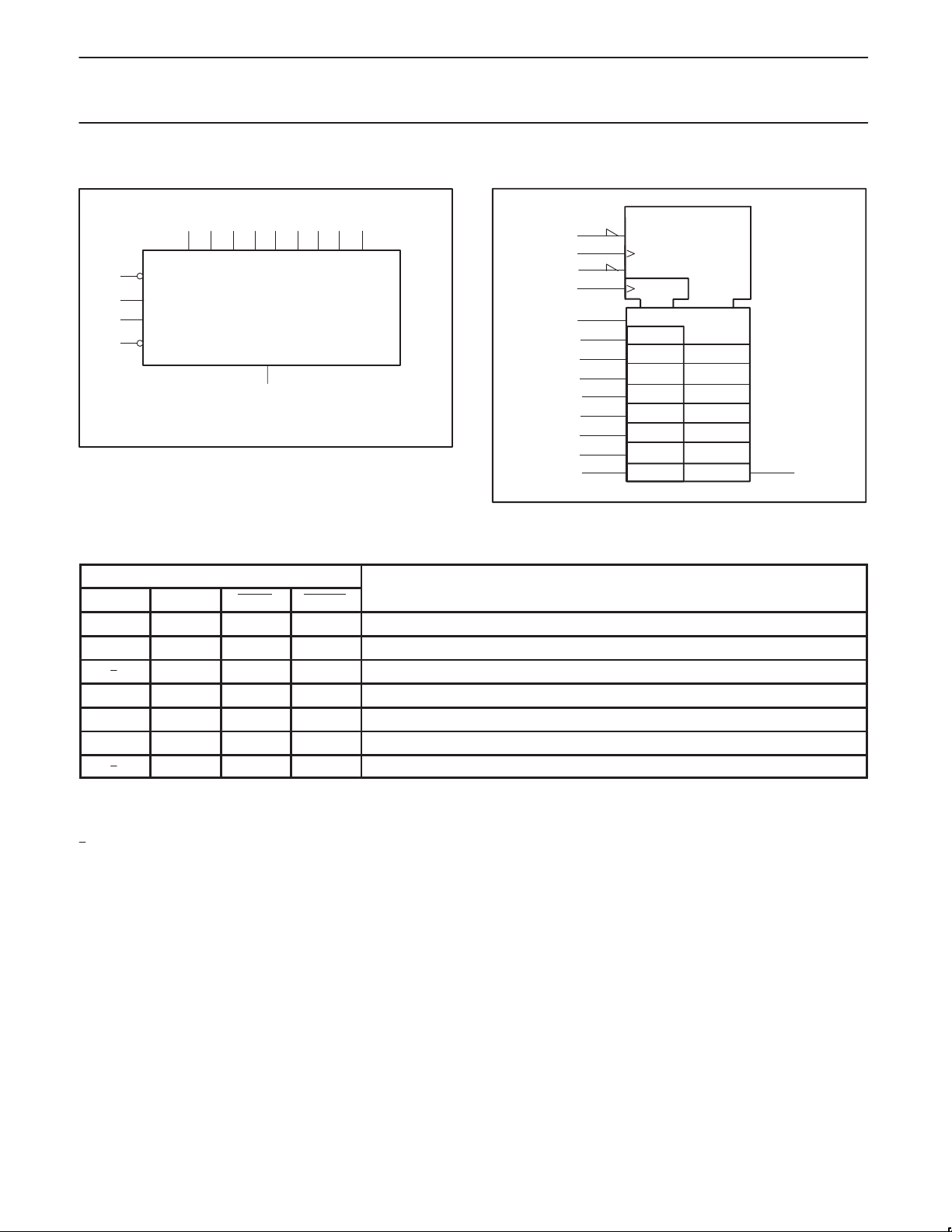
LOGIC SYMBOL
14
Ds
10
11
12
13
VCC= Pin 16
GND = Pin 8
SHRST
SHCP
STCP
SHLD
15 1 2 3
D0 D1 D2 D3
Qs
14
456
D4 D5 D67D7
SF01107
IEC/IEEE SYMBOL (IEEE/IEC)
10
11
13
12
14
15
1
2
3
4
5
6
7
SRG8
R
C3/
C2
C1
3D
1D
FUNCTION TABLE
INPUTS
STCP SHCP SHLD SHRST
↑ X X X Data loaded to storage registers
↑ L L H Data loaded from inputs to shift register
↑ L L H Data transferred from storage registers to shift registers
X L L L Invalid logic, state of shift register indeterminate when signals removed
X X H L Shift register cleared
X ↑ H H Shift register clocked, Qn=Qn–1, Q0=Ds
↑ H X H Hold
H = High voltage level
L = Low voltage level
X = Don’t care
↑ = Low-to-High clock transition
= Not a Low-to-High clock transition
↑
2D
9
SF01108
1991 Sep 13
3
Philips Semiconductors Product specification
74F5978-bit shift register with input storage registers
LOGIC DIAGRAM
10
SHRST
11
SHCP
13
SHLD
12
STCP
14
Ds
15
D0
1D
C2 2D
S
C1
1
D1
2
D2
3
D3
4
D4
5
D5
1D
C1
1D
C1
1D
C1
1D
C1
1D
C1
R
S
R
S
R
S
R
S
R
S
R
C2
C2 2D
C2 2D
C2 2D
C2 2D
2D
VCC = Pin 16
GND = Pin 8
1991 Sep 13
6
D6
7
D7
1D
C1
1D
C1
C2
S
R
C2 2D
S
R
2D
9
Qs
SF01109
4
 Loading...