

Philips N74F595N, N74F595D Datasheet
INTEGRATED CIRCUITS
74F595
8-bit shift register with output laches
(3-State)
Product specification
IC15 Data Handbook
1990 Apr 18
Philips Semiconductors Product specification
74F5958-bit shift register with output latches (3-State)
FEA TURES
•Low noise, now switching feedthrough current
•Controlled output edge rates
•High impedance PNP base inputs for reduced loading
(20µA in High and Low states)
•8-bit serial-in, parallel-out shift register with storage
•3-state outputs
•Shift register has direct clear
•Guaranteed shift frequency-DC to 100MHz
DESCRIPTION
The 74F595 contains an 8-bit serial-in, parallel-out shift register that
feeds an 8-bit D-type storage register. The storage register has
parallel 3-State outputs. Separate clocks are provided for both the
shift register and the storage register. The shift register has a direct
overriding clear, serial input and serial output pins for cascading.
Both the shift register and storage register clocks are positive
edge-triggered. If the user wishes to connect both clocks together,
the shift register state will always be one clock pulse ahead of the
storage register.
This device uses patented circuitry to control system noise and
internal ground bounce. This is done by eliminating switching
feedthrough current and controlling both Low-to-High and
High-to-Low slew rates.
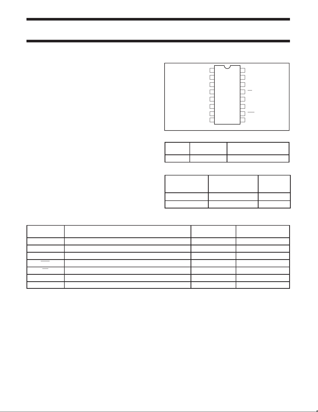
PIN CONFIGURATION
1
Q1
2
Q2
3
Q3
4
Q4
5
Q5
6
Q6
Q7
TYPE TYPICAL f
MAX
74F595 130MHz 65mA
16
V
CC
Q0
15
DS
14
OE
13
STCP
12
SHCP
11
SHR
107
98GND QS
SF01096
TYPICAL SUPPL Y CURRENT
(TOTAL)
ORDERING INFORMATION
COMMERCIAL RANGE
DESCRIPTION
16-pin plastic DIP N74F595N SOT38-4
16-pin plastic SO N74F595D SOT109-1
VCC = 5V ±10%,
= 0°C to +70°C
T
amb
PKG DWG #
INPUT AND OUTPUT LOADING AND FAN-OUT TABLE
PINS DESCRIPTION
Ds Serial data input 1.0/0.033 20µA/20µA
SHCP Shift register clock pulse input (active rising edge) 1.0/0.033 20µA/20µA
STCP Storage register clock pulse input (active rising edge) 1.0/0.033 20µA/20µA
SHR Shift register reset input (active Low) 1.0/0.033 20µA/20µA
OE Output Enable input (active Low) 1.0/0.033 20µA/20µA
Qs Serial expansion output 50/33 1.0mA/20mA
Q0–Q7 Data outputs 150/40 3.0mA/24mA
NOTE:
One (1.0) FAST unit load is defined as: 20µA in the High state and 0.6mA in the Low state.
74F (U.L.)
HIGH/LOW
LOAD VALUE
HIGH/LOW
1990 Apr 18 853–1096 99392
2
Philips Semiconductors Product specification
MODES
Shift
Store
Store, then Shift
74F5958-bit shift register with output latches (3-State)
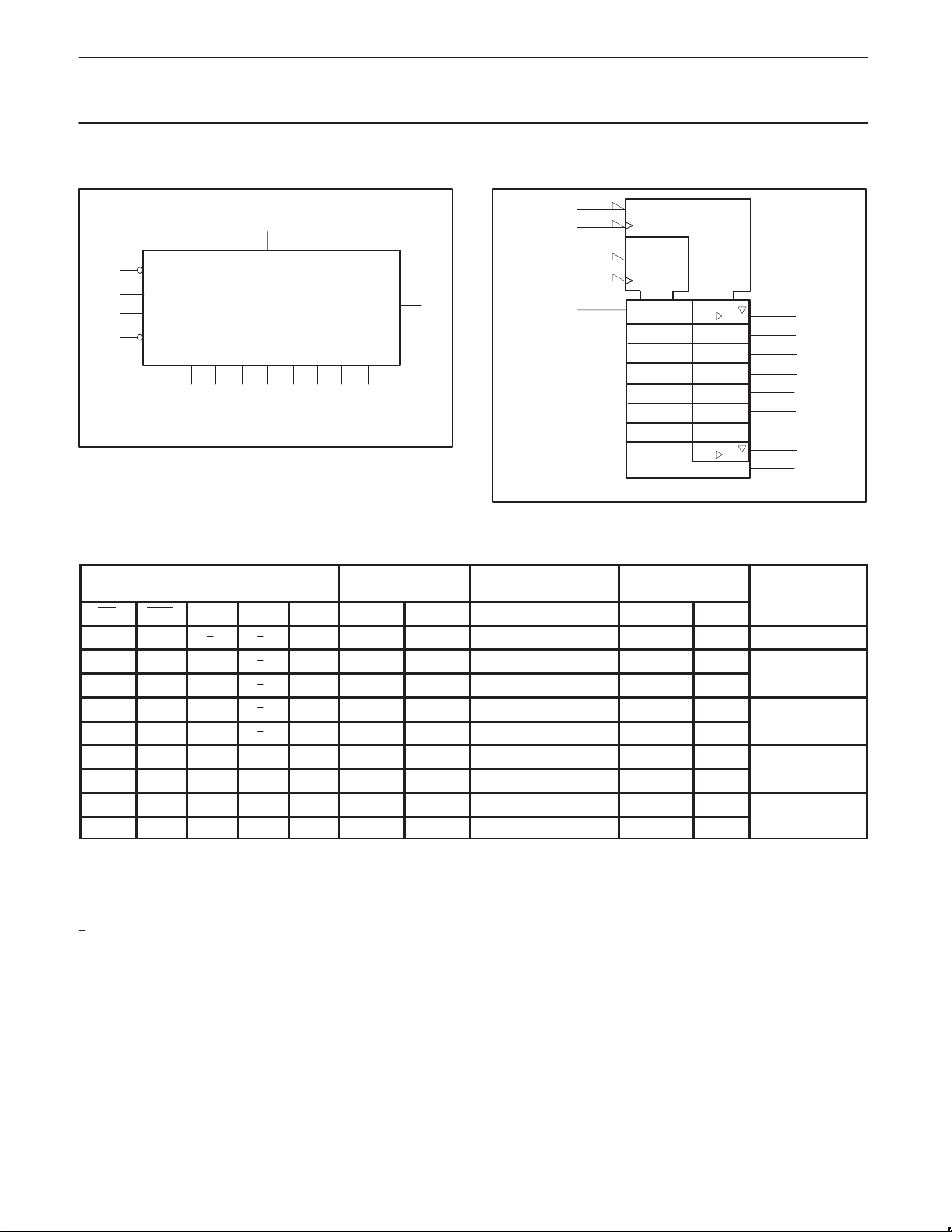
LOGIC SYMBOL
13
OE
12
STCP
11
SHCP
10
SHR
Q0 Q1 Q2 Q3
15 1 2 3
VCC= Pin 16
GND = Pin 8
14
Ds
Q4 Q5 Q67Q7
456
Qs
SF01097
9
IEC/IEEE SYMBOL (IEEE/IEC)
13
12
10
11
14
EN3
C2
SRG8
R
C1/
1D
3
2D
3
2D
15
1
2
3
4
5
6
7
9
SF01098
MODE SELECT – FUNCTION TABLE
INPUTS
INTERNAL SHIFT
REGISTERS
OE SHR SHCP STCP Dn O0 O1–O7 Q0–Q7 Q0–Q7 QS
H H ↑ ↑ X O0 O1–O7 Q0–Q7 Z Q7 No Change
H L X ↑ X L0 L Q0–Q7 Z L
L L X ↑ X L0 L Q0–Q7 Q0–Q7 L
H H ↑ ↑ ds Ds o0–o6 Q0–Q7 Z o6
L H ↑ ↑ ds Ds o0–o6 Q0–Q7 Q0–Q7 o6
H H ↑ ↑ X O0 O1–O7 o0–o7 Z Q7
L H ↑ ↑ X O0 O1–O7 o0–o7 o0–o7 Q7
H H ↑ ↑ ds Ds o0–o6 o0–o7* Z o6
L H ↑ ↑ ds Ds o0–o6 o0–o7* o0–o* o6
H = High voltage level
L = Low voltage level
X = Don’t care
Z = High impedance
dn (on)=Lower case letters indicate the state of the referenced input (or output) one setup time prior to the Low-to-High clock transition
↑ = Low-to-High clock transition
= Not a Low-to-High clock transition
↑
* = When clocking both SHCP and STCP simultaneously the Shift Register state will always be one clock pulse ahead of the Storage
Register
INTERNAL STORAGE
REGISTER
OUTPUTS
OPERATING
Clear shift
register, hold latch
1990 Apr 18
3
Philips Semiconductors Product specification
74F5958-bit shift register with output latches (3-State)
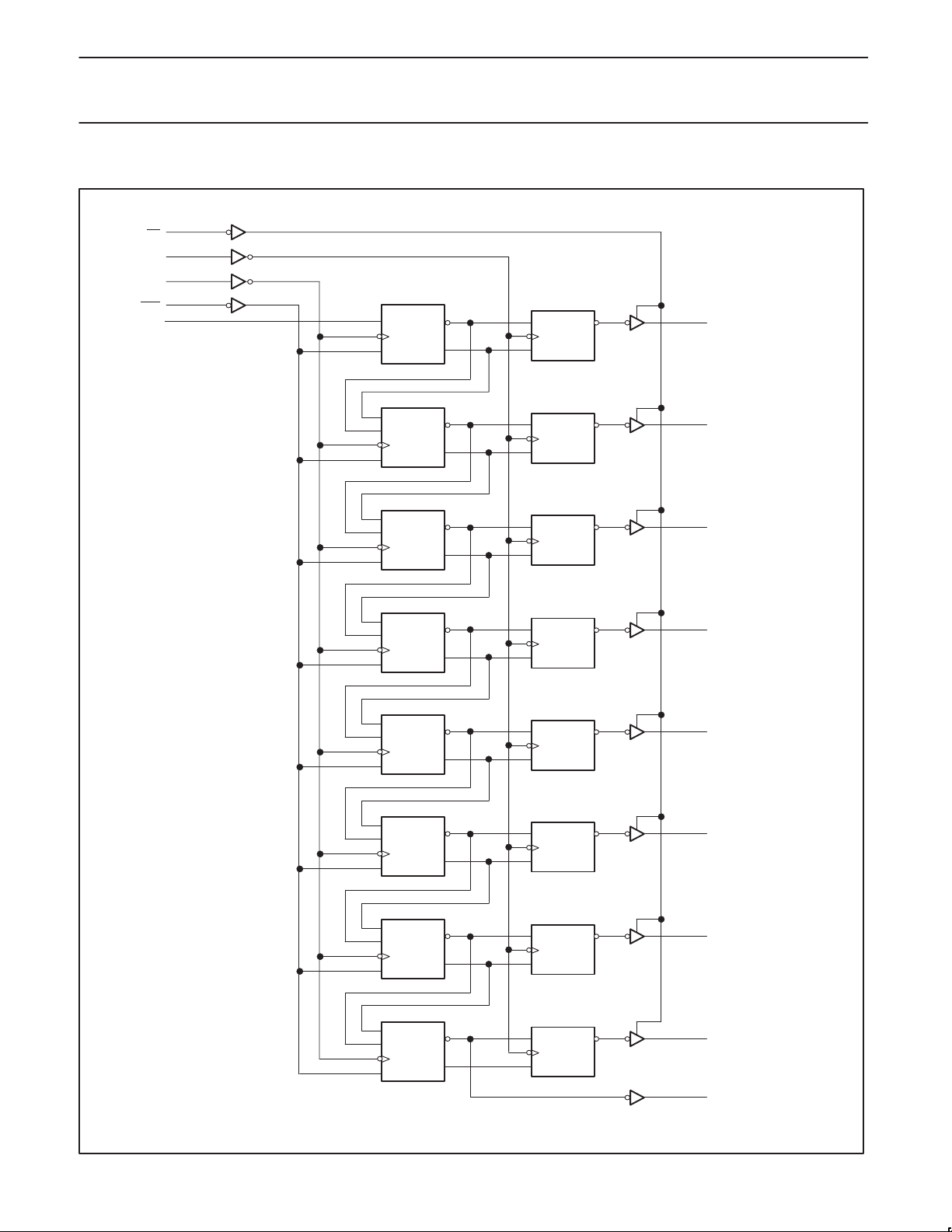
LOGIC DIAGRAM
13
OE
12
STCP
11
SHCP
10
SHR
14
Ds
D
CP
CLR
Q
Q
R
S
Q
CP
15
Q0
S
R
CP
CLR
S
R
CP
CLR
S
R
CP
CLR
S
R
CP
CLR
S
R
CP
CLR
1
Q
Q
Q
Q
Q
Q
Q
Q
Q
Q
CP
S
CP
S
CP
S
CP
S
CP
S
Q1RQ
2
Q2RQ
3
Q3RQ
4
Q4RQ
5
Q5RQ
VCC = Pin 16
GND = Pin 8
1990 Apr 18
S
R
CP
CLR
S
R
CP
CLR
6
7
9
SF01099
Q6RQ
Q7
Qs
Q
Q
Q
Q
CP
S
RQ
CP
S
4
 Loading...