

Philips N74F545N, N74F545D Datasheet

INTEGRATED CIRCUITS
74F545
Octal bidirectional transceiver (with
3-State inputs/outputs)
Product specification
IC15 Data Handbook
1990 Mar 01

Philips Semiconductors Product specification
74F545Octal bidirectional transceiver (with 3-State inputs/outputs)
FEA TURES
•High impedance NPN base inputs for reduced loading
(70µA in High and Low states) output
•8-bit bidirectional data flow reduces system package count
•3-State inputs/outputs for interfacing with bus oriented systems
•24mA and 64mA bus drive capability on A and B ports,
respectively
•Transmit/Receive and Output Enable simplify control logic
DESCRIPTION
The 74F545 is an 8-bit, 3-State, high speed transceiver. It provides
bidirectional drive for the bus-oriented microprocessor and digital
communications systems. Straight through bidirectional transceivers
are featured, with 24mA bus drive capability on the A ports and
64mA bus drive capability on the B ports. One input,
Transmit/Receive (T/R
through the bidirectional transceiver . Transmit enables data from A
ports to B ports; Receive enables data from B ports to A ports. The
Output Enable input disables both A and B ports by placing them in
a 3-State condition. The 74F545 performs the same function as the
74F245, the only difference being package pin assignment.
) determines the direction of logic signals
PIN CONFIGURATION
A0
1
A1
2
A2
3
A3
4
5
A4
A5
6
7
A6
A7
8
OE
9
10 11
GND
TYPE
TYPICAL
PROPAGATION DELAY
74F545 4.0ns 87mA
V
20
CC
B0
19
18
B1
17
B2
16
B3
B4
15
14
B5
13
B6
12
B7
T/R
SF01032
TYPICAL SUPPL Y
CURRENT
(TOTAL)
ORDERING INFORMATION
DESCRIPTION COMMERCIAL
RANGE
VCC = 5V ±10%,
T
= 0°C to +70°C
amb
20-Pin Plastic DIP N74F545N SOT146-1
20-Pin Plastic SOL N74F545D SOT163-1
PKG DWG #
INPUT AND OUTPUT LOADING AND FAN-OUT TABLE
PINS DESCRIPTION
74F(U.L.)
HIGH/LOW
A0–A7, B0–B7 Data inputs 3.5/0.1 17 70µA/70µA
OE Output Enable input (active Low) 2.0/0.067 40µA/40µA
T/R Transmit/Receive input 2.0/0.067 40µA/40µA
A0 - A7 Port A 3-State outputs 150/40 3.0mA/24mA
B0 - B7 Port B 3-State outputs 750/107 15mA/64mA
NOTE: One (1.0) FAST Unit Load is defined as: 20µA in the High state and 0.6mA in the Low state.
LOAD VALUE
HIGH/LOW
1990 Mar 01 853–0375 98992
2
Philips Semiconductors Product specification
74F545Octal bidirectional transceiver (with 3-State inputs/outputs)
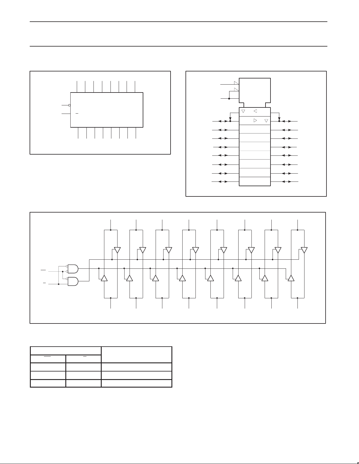
LOGIC SYMBOL
9
OE
11
T/R
= Pin 20
V
CC
GND = Pin 10
LOGIC DIAGRAM
234
A0 A1 A4 A5 A6 A7
B0 B1 B4 B5 B6 B7
18 17 16 15 14 13 12
19
56781
A3A2
B2 B3
SF01033
A0 A1 A4 A5 A6 A7
LOGIC SYMBOL (IEEE/IEC)
1
2
3
4
5
6
7
8
A3A2
234
9
11
56781
G3
3EN1
3EN2
1
2
19
18
17
16
15
14
13
12
SF01034
9
OE
11
T/R
19
VCC= Pin 20
GND = Pin 10
B0 B1 B4 B5 B6 B7
FUNCTION TABLE
INPUTS
OE T/R
L L Bus B data to Bus A
L H Bus A data to Bus B
H X Z
H = High voltage level
L = Low voltage level
X = Don’t care
Z = High impedance “off” state
18 17 16 15 14 13 12
B2 B3
SF01035
OUTPUTS
1990 Mar 01
3
 Loading...