

Philips N74F544D, N74F543D, N74F544N, N74F543N, N74F543DB Datasheet

INTEGRATED CIRCUITS
74F543
Octal registered transceiver,
non-inverting (3-State)
74F544
Octal registered transceiver,
inverting (3-State)
Product specification 1994 Dec 5
IC15 Data Handbook
Philips Semiconductors
Philips Semiconductors Product specification
74F543
74F543
74F544
74F543, 74F544Octal registered transceivers
74F543 Octal registered transceiver, non-inverting (3-State)
74F544 Octal registered transceiver, inverting 93-State)
FEA TURES
•Combines74F245 and 74F373 type functions in one chip
•8-bit octal transceiver with D-type latch
•74F543 Non-inverting
74F544 Inverting
•Back-to-back registers for storage
•Separate controls for data flow in each direction
•A outputs sink 20mA and source 3mA
•B outputs sink 64mA and source 15mA
•3-State outputs for bus-oriented applications
•74F543 available in SSOP Type II package
DESCRIPTION
The 74F543 and 74F544 Octal Registered Transceivers contain two
sets of D-type latches for temporary storage of data flowing in either
direction. Separate Latch Enable (LEAB
, OEBA) inputs are provided for each register to permit
(OEAB
independent control of inputting and outputting in either direction of
data flow. While the 74F543 has non-inverting data path, the 74F544
inverts data in both directions. The A outputs are guaranteed to sink
24mA, while the B outputs are rated for 64mA.
ORDERING INFORMATION
DESCRIPTION
24-pin plastic skinny DIP (300mil)
24-pin plastic SOL
24-pin plastic SSOP Type II 74F543DB SOT340-1
, LEBA) and Output Enable
COMMERCIAL RANGE
V
T
A
CC
= 0°C to +70°C
N74F543N,
N74F544N
N74F543D,
N74F544D
FUNCTIONAL DESCRIPTION
The 74F543 and 74F544 contain two sets of eight D-type latches,
with separate input and controls for each set. For data flow from A to
B, for example, the A-to-B Enable (EAB
to enter data from A0 - A7 or take data from B0 - B7, as indicated in
the Function Table. With EAB
Enable (LEAB
subsequent Low-to-High transition for the LEAB
A latches in the storage mode and their outputs no longer change
with the A inputs. With EAB
B output buffers are active and display the data present at the
outputs of the A latches. Control of data flow from B to A is similar,
but using the EBA
TYPE
74F543 6.0ns 80mA
74F544 6.5ns 95mA
= 5V ±10%,
) input makes the A-to-B latches transparent; a
, LEBA, and OEBA inputs.
TYPICAL
PROPAGATION
Low, a Low signal on the A-to-B Latch
and OEAB both Low, the 3-State
DELA Y
) input must be Low in order
signal puts the
TYPICAL
SUPPLY CURRENT
(TOTAL)
DRAWING
NUMBER
SOT222–1
SOT137-1
INPUT AND OUTPUT LOADING AND FAN-OUT TABLE
PINS DESCRIPTION
A0 - A7 Port A, 3-State inputs 3.5/1.0 70µA/0.6mA
B0 - B7 Port B, 3-State inputs 3.5/1.0 70µA/0.6mA
OEAB A-to-B Output Enable input (Active Low) 1.0/1.0 20µA/0.6mA
74F543
74F544
NOTE: One (1.0) FAST Unit Load is defined as: 20µA in the High State and 0.6mA in the Low state.
1994 Dec 5 853-0874 14379
OEBA B-to-A Output Enable input (Active Low) 1.0/1.0 20µA/0.6mA
EAB A-to-B Enable input (Active Low) 1.0/2.0 20µA/1.2mA
EBA B-to-A Enable input (Active Low) 1.0/2.0 20µA/1.2mA
LEAB A-to-B Latch Enable input (Active Low) 1.0/1.0 20µA/0.6mA
LEBA B-to-A Latch Enable input (Active Low) 1.0/1.0 20µA/0.6mA
A0 - A7 Port A, 3-State outputs 150/40 3.0mA/24mA
B0 - B7 Port B, 3-State outputs 750/106.7 15mA/64mA
A0 - A7 Port A, 3-State outputs 150/40 3.0mA/24mA
B0 - B7 Port B, 3-State outputs 750/106.7 15mA/64mA
2
74F(U.L.)
HIGH/LOW
LOAD VALUE
HIGH/LOW
Philips Semiconductors Product specification
74F543, 74F544Octal registered transceivers
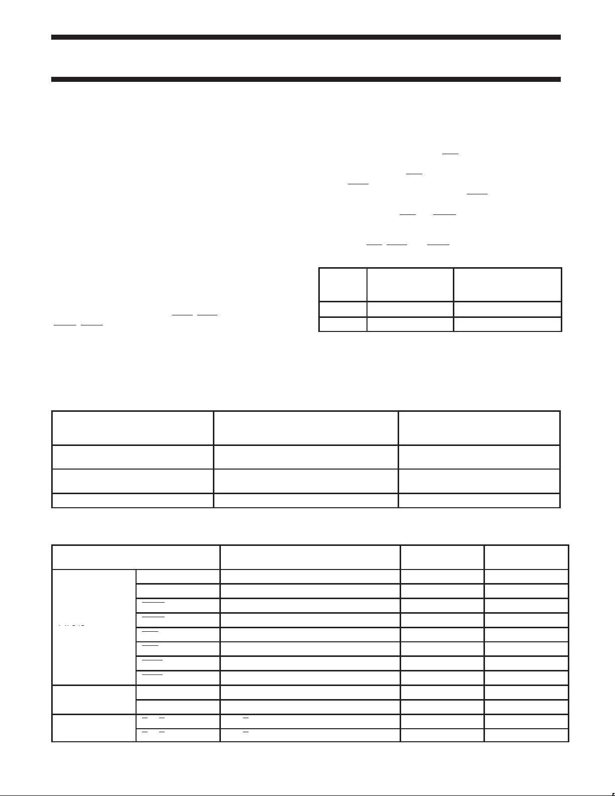
PIN CONFIGURATION – 74F543
LEBA
1
OEBA
2
3
A0
4
A1
5
A2
6
A3
7
A4
8
A5
9
A6
10
A7
EAB LEAB
11
GND
24
V
EBA
23
22
B0
21
B1
20
B2
19
B3
18
B4
17
B5
16
B6
15
B7
14
OEAB
1312
SF00237
CC
LOGIC SYMBOL (IEEE/IEC) – 74F543
2
23
1
13
11
14
IEN3
G1
1C5
2EN4
G2
2C6
LOGIC SYMBOL – 74F543
345678910
A0 A1 A2 A3 A4 A5 A6 A7
EAB
11
23
EBA
LEAB
14
LEBA
1
B0 B1 B2 B3 B4 B5 B6 B7
= Pin 24
V
CC
GND = Pin 12
22 21 20 19 18 17 16 15
OEAB
OEBA
13
2
SF00238
3
4
5
6
7
8
9
10
35D
46D
22
21
20
19
18
17
16
15
SF00239
1994 Dec 5
3
Philips Semiconductors Product specification
Disable +
Latch +
Transparent
74F543, 74F544Octal registered transceivers
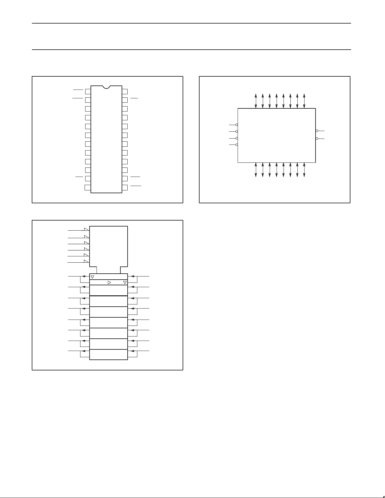
PIN CONFIGURATION – 74F544
LEBA
1
OEBA
2
3
A
0
4
A
1
5
2
A
6
A3
7
A
4
8
5
A
9
A
6
10
7
A
EAB LEAB
11
GND
24
V
EBA
23
22
B0
21
B
20
B
19
B3
18
B
17
B
16
B
15
B
14
OEAB
1312
SF00240
CC
1
2
4
5
6
7
LOGIC SYMBOL (IEEE/IEC) – 74F544
2
23
1
13
11
14
3
4
5
6
7
8
9
10
IEN3
G1
1C5
2EN4
G2
2C6
35D
46D
SF00241
LOGIC SYMBOL – 74F544
345678910
A0 A1 A2 A3 A4 A5 A6 A7
EAB
11
23
14
1
= Pin 24
V
CC
GND = Pin 12
EBA
LEAB
LEBA
B0 B1 B2 B3 B4 B5 B6 B7
22 21 20 19 18 17 16 15
OEAB
OEBA
13
2
SF00242
FUNCTION TABLE for 74F543 and 74F544
INPUTS OUTPUTS STATUS
OEXX EXX LEXX DATA 74F543 74F544
H X X X Z Z Disabled
X H X X Z Z Disabled
L ↑ L h Z Z
L ↑ L l Z Z
22
21
20
L L ↑ h H L
L L ↑ l L H
L L L H H L
L L L L L H
19
18
17
16
15
L L H X NC NC Hold
H = High voltage level
L = Low voltage level
h = High state must be present one setup time before the
Low-to-High transition of LEXX
or EXX (XX=AB or BA)
l = Low state must be present one setup time before the
Low-to-High transition of LEXX
↑ = Low-to-High transition of LEXX
or EXX (XX=AB or BA)
or EXX XX = AB or BA
X = Don’t care
NC = No change
Z = High impedance “off” state
Disable +
Latch
Latch +
Display
p
1994 Dec 5
4
Philips Semiconductors Product specification
74F543, 74F544Octal registered transceivers
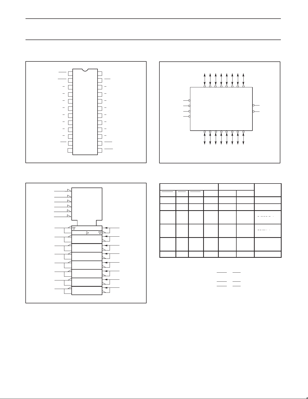
LOGIC DIAGRAM FOR 74F543
OEBA
EBA
VCC = Pin 24
GND = Pin 12
LEBA
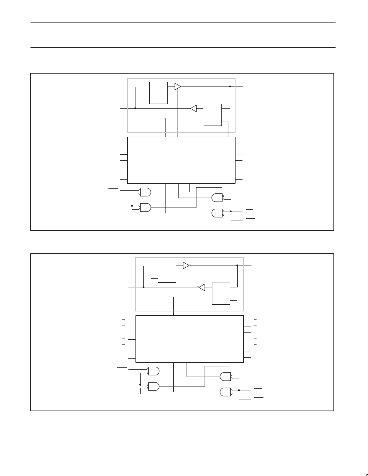
LOGIC DIAGRAM FOR 74F544
QD
LE
3
A0
4
A1
5
A2
6
A3
7
A4
8
A5
9
A6
10
A7
2
23
1
DETAIL A X 7
DETAIL A
QD
LE
22
B0
21
B1
20
B2
19
B3
18
B4
17
B5
16
B6
15
B7
13
OEAB
11
EAB
14
LEAB
SF00243
VCC = Pin 24
GND = Pin 12
OEBA
EBA
LEBA
QD
LE
3
0
A
4
A
1
5
A
2
6
A
3
7
4
A
8
A
5
9
6
A
10
A
7
2
23
1
DETAIL A X 7
DETAIL A
QD
LE
22
B0
21
B
20
B
19
B
18
B
17
B
16
B
15
B
13
OEAB
11
EAB
14
LEAB
SF00244
1
2
3
4
5
6
7
1994 Dec 5
5
 Loading...