

Philips N74F534D, N74F533D, N74F534N, N74F533N Datasheet

74F533*,74F534
Latch/flip-flop
Product specification
Supersedes data of 1989 May 11
IC15 Data Handbook
1999 Jan 08
INTEGRATED CIRCUITS
* Discontinued part. Please see the Discontinued Product List.
Philips Semiconductors Product specification
74F533,* 74F534Latch/flip-flop
74F533 Octal Transparent Latch, Inverting (3-State)
74F534 Octal D Flip-Flop, Inverting (3-State)
2
1999 Jan 08 853-0374 20616
* Discontinued part. Please see the Discontinued Products List.
FEA TURES
•8-bit positive edge-triggered register – 74F534
•3-State inverting output buffers
•Common 3-State Output register
•Independent register and 3-State buffer operation
DESCRIPTION
The 74F533 is an octal transparent latch coupled to eight 3-State
output buffers. The two sections of the device are controlled
independently by Enable (E) and Output Enable (OE) control gates.
The data on the D inputs is transferred to the latch outputs when the
Enable (E) input is High. The latch remains transparent to the data
input while E is High and stores the data that is present one setup
time before the High-to-Low enable transition.
The 3-State output buffers are designed to drive heavily loaded
3-State buses, MOS memories, or MOS microprocessors. The
active Low Output Enable (OE
) controls all eight 3-State buffers
independent of the latch operation. When OE
is Low, the latched or
transparent data appears at the outputs. When OE
is High, the
outputs are in high impedance “off” state, which means they will
neither drive nor load the bus.
The 74F534 is an 8-bit edge-triggered register coupled to eight
3-State output buffers. The two sections of the device are controlled
independently by the Clock (CP) and Output Enable (OE
) control
gates.
The register is fully edge-triggered. The state of each D input, one
setup time before the Low-to-High clock transition is transferred to
the corresponding flip-flop’s Q
output.
The 3-State output buffers are designed to drive heavily loaded
3-State buses, MOS memories, or MOS microprocessors. The
active Low Output Enable (OE
) controls all eight 3-State buffers
independent of the latch operation. When OE
is Low, the latched or
transparent data appears at the outputs. When OE
is High, the
outputs are in high impedance “off” state, which means they will
neither drive nor load the bus.
TYPE
TYPICAL
PROPAGATION DELAY
TYPICAL SUPPL Y
CURRENT
(TOT AL)
74F533 5.5ns 41mA
TYPE TYPICAL f
MAX
TYPICAL SUPPL Y
CURRENT
(TOT AL)
74F534 165MHz 51mA
ORDERING INFORMATION
DESCRIPTION
COMMERCIAL
RANGE
VCC = 5V ±10%,
T
amb
= 0°C to +70°C
PKG DWG #
20-Pin Plastic DIP N74F534N SOT146-1
20-Pin Plastic SOL N74F534D SOT163-1
INPUT AND OUTPUT LOADING AND FAN-OUT TABLE
PINS DESCRIPTION
74F (U.L.)
HIGH/LOW
LOAD VALUE
HIGH/LOW
D0 - D7 Data inputs 1.0/1.0 20µA/0.6mA
E (74F533) Enable input (active High) 1.0/1.0 20µA/0.6mA
OE Output Enable input (active Low) 1.0/1.0 20µA/0.6mA
CP (74F534) Clock Pulse input (active rising edge) 1.0/1.0 20µA/0.6mA
Q0 - Q7 Data outputs 150/40 3.0mA/24mA
Philips Semiconductors Product specification
74F533,* 74F534Latch/flip-flop
1999 Jan 08
3
* Discontinued part. Please see the Discontinued Products List.
NOTE: One (1.0) FAST Unit Load (U.L.) is defined as: 20µA in the High state and 0.6mA in the Low state.
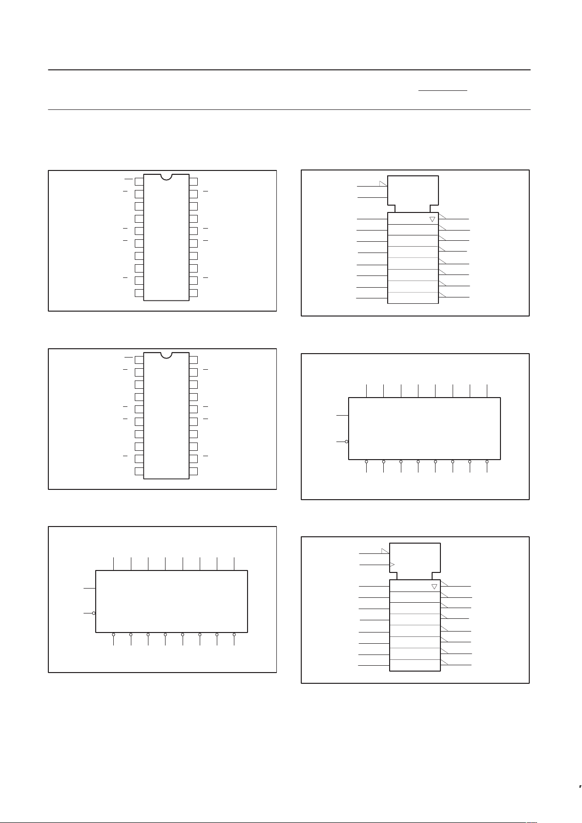
PIN CONFIGURATION – 74F533
1
2
3
4
5
6
7
8
9
10 11
12
13
14
15
16
17
18
19
20
OE
Q0
D0
D1
Q
1
Q
2
D2
D3
Q
3Q4
GND
D4
D5
Q
5
Q
6
D6
D7
Q
7
V
CC
E
SF00981
PIN CONFIGURATION – 74F534
1
2
3
4
5
6
7
8
9
10 11
12
13
14
15
16
17
18
19
20
OE
Q0
D0
D1
Q
1
Q
2
D2
D3
Q
3Q4
GND
D4
D5
Q
5
Q
6
D6
D7
Q
7
V
CC
CP
SF00982
LOGIC SYMBOL – 74F533
34781314
15129652
1
11
E
OE
Q0
D0 D1Q1D2
Q2 Q3D3Q4D4Q5
D5
17 18
1916
Q6D6Q7
D7
SF00983
VCC=Pin 20
GND=Pin 10
LOGIC SYMBOL (IEEE/IEC) – 74F533
3
4
7
8
13
14
17
18
1
11
2D
2
5
6
9
12
15
16
19
EN1
EN2
1
SF00985
LOGIC SYMBOL – 74F534
34781314
15129652
1
11 CP
OE
Q0
D0 D1Q1D2
Q2 Q3D3Q4D4Q5
D5
17 18
1916
Q6D6Q7
D7
SF00984
VCC=Pin 20
GND=Pin 10
LOGIC SYMBOL (IEEE/IEC) – 74F534
3
4
7
8
13
14
17
18
1
11
2D
2
5
6
9
12
15
16
19
EN1
C1
1
SF00986

Philips Semiconductors Product specification
74F533,* 74F534Latch/flip-flop
1999 Jan 08
4
* Discontinued part. Please see the Discontinued Products List.
LOGIC DIAGRAM – 74F533
D0 D1 D2 D3 D4 D5 D6 D7
Q
0Q1Q2Q3Q4Q5Q6Q7
E
OE
3 4 7 8 13 14 17 18
191615129652
1
11
EDQ EDQ EQDEDQ EDQ EDQ EDQ EDQ
VCC=Pin 20
GND=Pin 10
SF00987
LOGIC DIAGRAM – 74F534
D0 D1 D2 D3 D4 D5 D6 D7
Q
0Q1Q2Q3Q4Q5Q6Q7
CP
OE
3 4 7 8 13 14 17 18
191615129652
1
11
CPDQ CPDQ CP Q
D
CPDQ CPDQ CPDQ CPDQ CPDQ
VCC=Pin 20
GND=Pin 10
SF00988
FUNCTION TABLE – 74F533
INPUTS
INTERNAL
OUTPUTS
OE E Dn
REGISTER
Q0 – Q7
OPERATING MODES
L
L
H
H
L
H
L
H
H
L
Load and read register
L
L
↓
↓
l
h
L
H
H
L
Enable and read register
L L X NC NC Hold
H
H
L
H
X
Dn
NC
Dn
Z
Z
Disable outputs
H = High voltage level
h = High voltage level one setup time prior to the High-to-Low E transition
L = Low voltage level
l = Low voltage level one setup time prior to the High-to-Low E transition
NC= No change
X = Don’t care
Z = High impedance “off” state
↓ = High-to-Low E transition
 Loading...