

Philips N74ALS645A-1D, N74ALS645A-1N, N74ALS645AD, N74ALS645AN Datasheet
74ALS645A/74ALS645A–1
Octal transceiver (3–State)
Product specification
IC05 Data Handbook
1991 Jun 03
INTEGRATED CIRCUITS
Philips Semiconductors Product specification
74ALS645A/74ALS645A-1Octal transceiver (3-State)
2
1991 Jun 03 853–0597 02709
FEA TURES
•Octal bidirectional bus interface
•3-State buffer outputs sink 24mA and source 15mA
•Outputs are placed in high impedance state during power-off
conditions
•The -1 version sinks 48mA I
OL
within the +5% VCC range
DESCRIPTION
The 74ALS645A is an octal transceiver featuring non-inverting
3-State bus compatible outputs in both transmit and receive
directions. The device features an output enable (OE) input for easy
cascading and transmit/receive (R/T
) input for direction control.
The 74ALS645A-1 is the same as the 74ALS645A except that both
ports sink 48mA within the ±5% V
CC
range.
TYPE
TYPICAL
PROPAGATION
DELA Y
TYPICAL
SUPPLY CURRENT
(TOTAL)
74ALS645A 7.0ns 34mA
74ALS645A-1 7.0ns 34mA
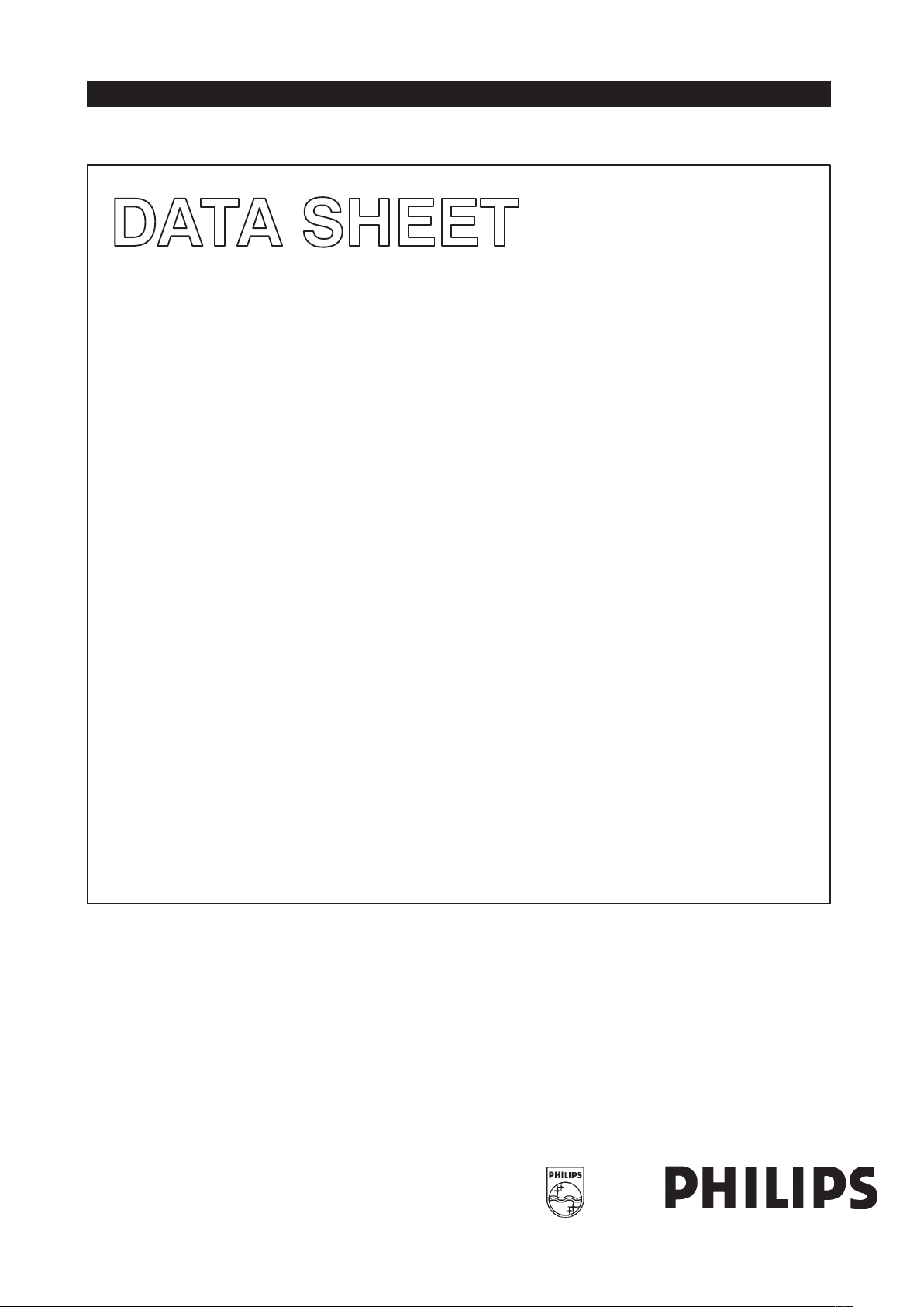
PIN CONFIGURATION
SF00198
1
2
3
4
5
6
7
8
9
10 11
12
13
14
15
16
17
18
19
20
T/R
A0
A1
A2
A3
A4
A5
A6
A7
GND
V
CC
OE
B0
B1
B2
B3
B4
B6
B5
B7
ORDERING INFORMA TION
ORDER CODE
DESCRIPTION
COMMERCIAL RANGE
V
CC
= 5V ±10%,
T
amb
= 0°C to +70°C
DRAWING
NUMBER
20-pin plastic DIP
74ALS645AN,
74ALS645A-1N
SOT146-1
20-pin plastic SOL
74ALS645AD,
744ALS645A-1D
SOT163-1
INPUT AND OUTPUT LOADING AND FAN-OUT TABLE
PINS DESCRIPTION
74ALS (U.L.)
HIGH/LOW
LOAD VALUE
HIGH/LOW
A0 – A7, B0 – B7 Data inputs 1.0/1.0 20µA/0.1mA
OE Output Enable input (active-Low) 1.0/1.0 20µA/0.1mA
T/R T ransmit/receive input 1.0/1.0 20µA/0.1mA
A0 – A7 A port outputs 750/240 15mA/24mA
B0 – B7 B port outputs 750/240 15mA/24mA
A0 – A7 A port outputs (-1 version) 750/480 15mA/48mA
B0 – B7 B port outputs (-1 version) 750/480 15mA/48mA
NOTE: One (1.0) ALS unit load is defined as: 20µA in the High state and 0.1mA in the Low state.
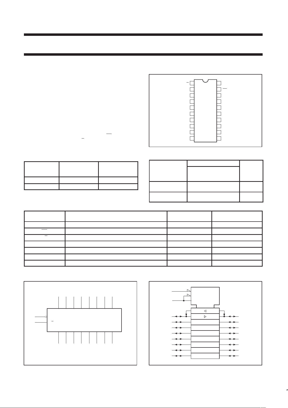
LOGIC SYMBOL
B2 B3 B4 B5
16 15 14 13
234
V
CC
= Pin 20
GND = Pin 10
SF00199
B1
17
B0
18
19
1
OE
T/R
A0 A1 A2 A3 A4 A5
567
B6 B7
12 11
A6 A7
89
IEC/IEEE SYMBOL
SC00097
G3
19
3EN1 [BA]
1
3EN2 [AB]
∇ 1
2 ∇
2
3
4
5
6
7
8
9
18
17
16
15
14
13
12
11
Philips Semiconductors Product specification
74ALS645A/74ALS645A-1Octal transceiver (3-State)
1991 Jun 03
3
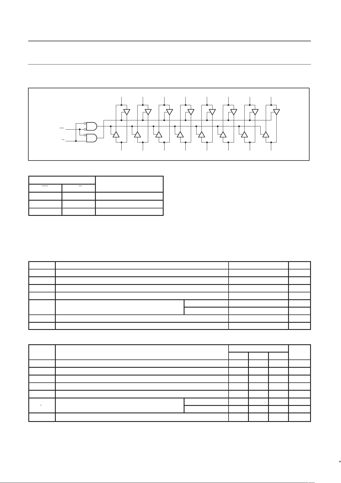
LOGIC DIAGRAM
SF00201
18
B0
17
B1
16
B2
15
B3
14
B4
13
B5
12
B6
11
B7
A0 A1 A2 A3 A4 A5 A6 A7
23456789
19
1
OE
T/R
VCC = Pin 20
GND = Pin 10
FUNCTION TABLE
INPUTS
OE T/R
OUTPUTS
L L Bus B data to Bus A
L H Bus A data to Bus B
H X Z
H = High voltage level
L = Low voltage level
X = Don’t care
Z = High impedance “off” state
ABSOLUTE MAXIMUM RATINGS
(Operation beyond the limit set forth in this table may impair the useful life of the device.
Unless otherwise noted these limits are over the operating free air temperature range.)
SYMBOL
PARAMETER RATING UNIT
V
CC
Supply voltage –0.5 to +7.0 V
V
IN
Input voltage –0.5 to +7.0 V
I
IN
Input current –30 to +5 mA
V
OUT
Voltage applied to output in High output state –0.5 to V
CC
V
pp
p
p
All versions 48 mA
I
OUT
Current applied to output in Low output state
-1 version 96 mA
T
amb
Operating free-air temperature range 0 to +70 °C
T
stg
Storage temperature range –65 to +150 °C
RECOMMENDED OPERATING CONDITIONS
LIMITS
SYMBOL
PARAMETER
MIN NOM MAX
UNIT
V
CC
Supply voltage 4.5 5.0 5.5 V
V
IH
High-level input voltage 2.0 V
V
IL
Low-level input voltage 0.8 V
I
IK
Input clamp current –18 mA
I
OH
High-level output current –15 mA
p
All versions 24 mA
IOLLow-level output current
-1 version 48
1
mA
T
amb
Operating free-air temperature range
0 +70 °C
NOTES:
1. The 48mA limit applies only under the condition of V
CC
= 5.0V ± 5%.
 Loading...