

Philips N74ALS157D, N74ALS158D, N74ALS158N Datasheet
74ALS157/74ALS158
Data selector/multiplexer
Product specification
IC05 Data Handbook
1991 Feb 08
INTEGRATED CIRCUITS
Philips Semiconductors Product specification
74ALS157/74ALS158Data selector/multiplexer
74ALS157 Quad 2-input data selector/multiplexer, non-inverting
74ALS158 Quad 2-input data selector/multiplexer, inverting
2
1991 Feb 08 853–1 129 01670
DESCRIPTION
The 74ALS157 is a quad 2-input multiplexer which selects 4 bits of
data from one of two sources under the control of a common select
input (S). The enable input (E
) is active when Low. When E is High,
all of the outputs (Yn) are forced Low regardless of all other input
conditions.
Moving data from two registers to a common output bus is a typical
use of the 74ALS157. The state of the select input determines the
particular register from which data comes.
The device is the logic implementation of 4-pole, 2-position switch
where the position of the switch is determined by the logic levels
supplied to the select input. The 74ALS158 is similar but has
inverting outputs (Y
n).
TYPE
TYPICAL
PROPAGATION DELAY
TYPICAL
SUPPLY CURRENT
(TOTAL)
74ALS157 6.0ns 6mA
74ALS158 6.0ns 6mA
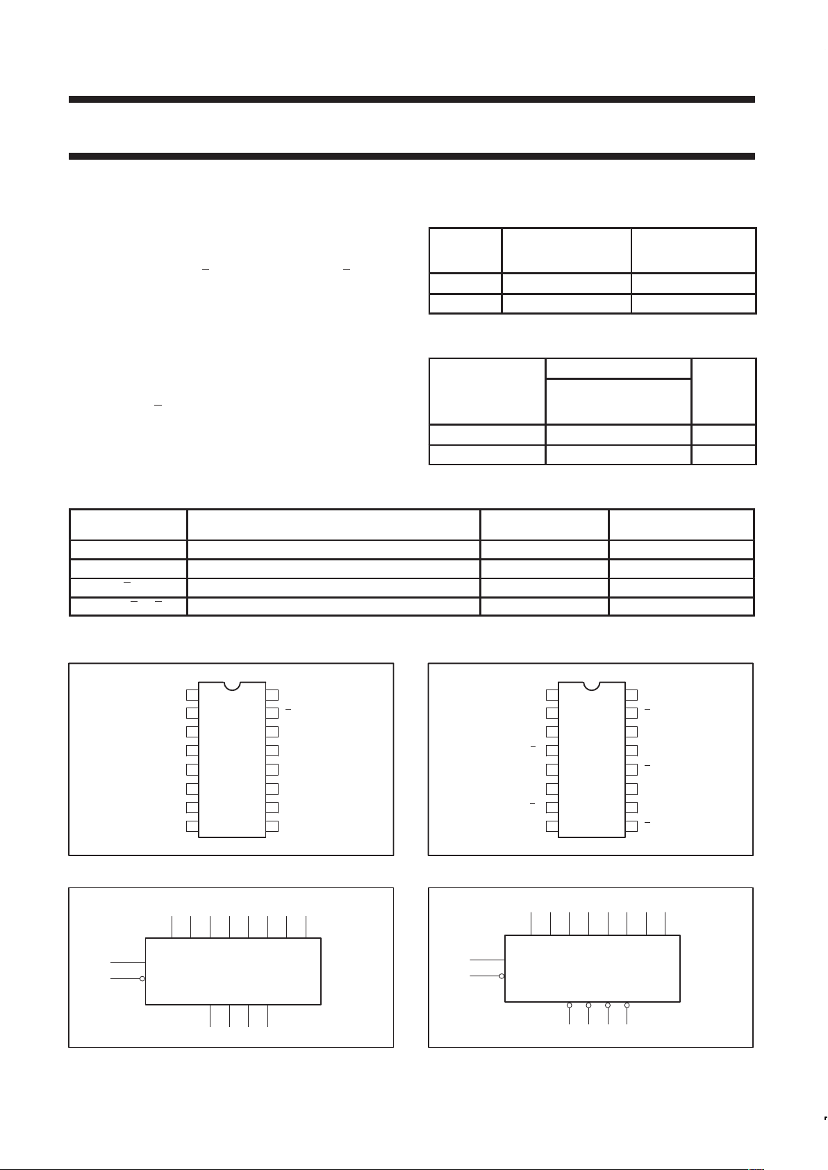
ORDERING INFORMATION
ORDER CODE
DESCRIPTION COMMERCIAL RANGE
V
CC
= 5V ±10%,
T
amb
= 0°C to +70°C
DRAWING
NUMBER
16-pin plastic DIP 74ALS157N, 74ALS158N SOT38-4
16-pin plastic SO 74ALS157D, 74ALS158D SOT109-1
INPUT AND OUTPUT LOADING AND FAN-OUT TABLE
PINS DESCRIPTION
74ALS (U.L.)
HIGH/LOW
LOAD VALUE
HIGH/LOW
Ina, Inb, Inc, Ind Data inputs 1.0/1.0 20µA/0.1mA
S Select input 1.0/1.0 20µA/0.1mA
E Enable input 1.0/1.0 20µA/0.1mA
Ya – Yd, Ya – Yd Data outputs 20/240 0.4mA/24mA
NOTE: One (1.0) ALS unit load is defined as: 20µA in the High state and 0.1mA in the Low state.
PIN CONFIGURATION – 74ALS157
16
15
14
13
12
11
107
6
5
4
3
2
1
Yb
V
CC
Yd
I0c
I1c
I1d
E
I0d
S
I0a
I1b
I1a
Ya
I0b
98GND Yc
SC00051
PIN CONFIGURATION – 74ALS158
16
15
14
13
12
11
107
6
5
4
3
2
1
Y
b
V
CC
Yd
I0c
I1c
I1d
E
I0d
S
I0a
I1b
I1a
Y
a
I0b
98GND Yc
SC00052
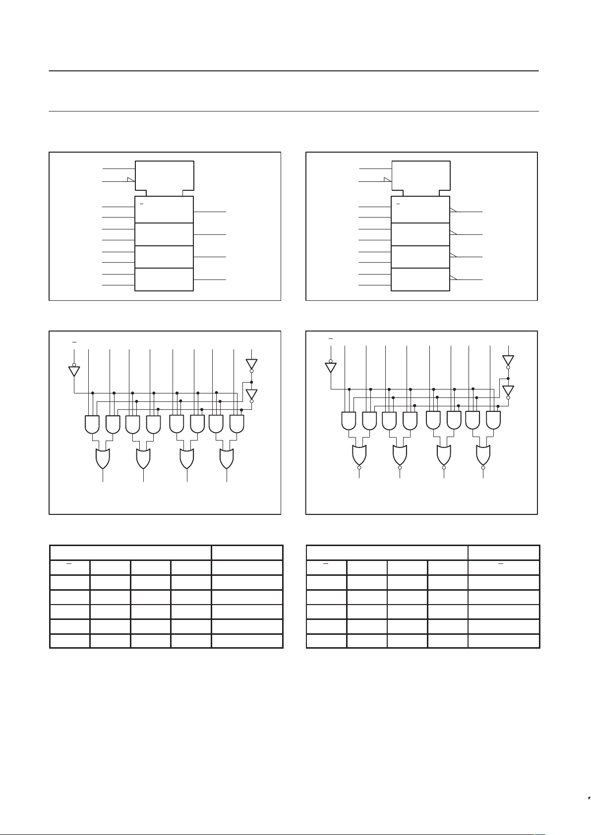
LOGIC SYMBOL – 74ALS157
VCC = Pin 16
GND = Pin 8
SC00053
1
15
S
E
2356111014
I0a I1a I0b I1b I0c I1c I0d
Ya Yb Yc Yd
47912
13
I1d
LOGIC SYMBOL – 74ALS158
VCC = Pin 16
GND = Pin 8
SC00054
1
15
S
E
2356111014
I0a I1a I0b I1b I0c I1c I0d
Ya Yb Yc Yd
47912
13
I1d
Philips Semiconductors Product specification
74ALS157/74ALS158Data selector/multiplexer
1991 Feb 08
3
IEC/IEEE SYMBOL – 74ALS157
SC00055
2
1
1
G1
15
EN
3
4
1
MUX
5
6
7
11
10
9
14
13
12
IEC/IEEE SYMBOL – 74ALS158
SC00056
2
1
1
G1
15
EN
3
4
1
MUX
5
6
7
11
10
9
14
13
12
LOGIC DIAGRAM – 74ALS157
VCC = Pin 16
GND = Pin 8
E I0a I1a I0b I1b I0c I1c I0d I0d S
15 2 3 5 6 11 10 14 13 1
47 912
Ya Yb Yc Yd
SC00057
LOGIC DIAGRAM – 74ALS158
VCC = Pin 16
GND = Pin 8
E I0a I1a I0b I1b I0c I1c I0d I0d S
15 2 3 5 6 11 10 14 13 1
47 912
Ya Yb Yc Yd
SC00058
FUNCTION T ABLE – 74ALS157
INPUTS OUTPUTS
E S I0n I1n Yn
H X X X L
L L L X L
L L H X H
L H X L L
L H X H H
H = High voltage level
L = Low voltage level
X = Don’t care
FUNCTION T ABLE – 74ALS158
INPUTS OUTPUTS
E S I0n I1n Yn
H X X X H
L L L X H
L L H X L
L H X L H
L H X H L
H = High voltage level
L = Low voltage level
X = Don’t care
 Loading...