

Philips N74ALS153D, N74ALS153DB, N74ALS153N Datasheet

74ALS153
Dual 4-input multiplexer
Product specification 1991 Feb 08
INTEGRATED CIRCUITS
IC05 Data Handbook
Philips Semiconductors Product specification
74ALS153Dual 4-input multiplexer
2
1991 Feb 08 853–1376 01670
FEA TURES
•Non–inverting outputs
•Common select outputs
•Separate enable for each section
•See 74ALS253 for 3–State version
DESCRIPTION
The 74ALS153 has two identical 4–input multiplexer with 3–State
outputs which selects two bits of data from four sources by using
common select inputs (S0, S1). The two 4–input multiplexer circuits
have individual active–Low enables (E
a, Eb) which can be used to
strobe the outputs independently. Outputs (Ya, Yb) are forced Low
when the corresponding enable is high.
The 74ALS153 is the logic implementation of a 2–pole, 4–position
switch where the position of the switch is determined by the logic
levels supplied to the common select inputs.
TYPE
TYPICAL
PROPAGATION DELAY
TYPICAL
SUPPLY CURRENT
(TOTAL)
74ALS153 7.0ns 6.5mA
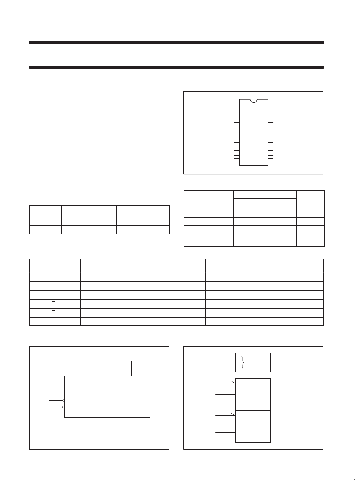
PIN CONFIGURATION
16
15
14
13
12
11
107
6
5
4
3
2
1
Ya
V
CC
I2b
I1b
I0b
I3b
E
b
S0
E
a
S1
I0a
I3a
I2a
I1a
98GND Yb
SF00146
ORDERING INFORMA TION
ORDER CODE
DESCRIPTION COMMERCIAL RANGE
V
CC
= 5V ±10%,
T
amb
= 0°C to +70°C
DRAWING
NUMBER
16-pin plastic DIP 74ALS153N SOT38-4
16-pin plastic SO 74ALS153D SOT109-1
16-pin plastic SSOP
Type II
74ALS153DB SOT338-1
INPUT AND OUTPUT LOADING AND FAN-OUT TABLE
PINS DESCRIPTION
74ALS (U.L.)
HIGH/LOW
LOAD VALUE
HIGH/LOW
Ioa – I3a Port A data inputs 1.0/1.0 20µA/0.1mA
Iob – I3b Port B data inputs 1.0/1.0 20µA/0.1mA
S0, S1 Common select inputs 1.0/1.0 20µA/0.1mA
Ea Port A enable input 1.0/1.0 20µA/0.1mA
Eb Port B enable input 1.0/1.0 20µA/0.1mA
Ya, Yb Data outputs 130/240 2.6mA/24mA
NOTE: One (1.0) ALS unit load is defined as: 20µA in the High state and 0.1mA in the Low state.
LOGIC SYMBOL
Ya
7
V
CC
= Pin 16
GND = Pin 8
14
2
1
15
S0
S1
Ea
Eb
I1a I2a
43
SF00147
I3aI0a
65
Yb
9
I1b I2b
12 13
I3bI0b
10 11
IEC/IEEE SYMBOL
SF00148
1
6
5
EN
0
1
14
0
2
1
7
G
0
3
MUX
4
3
2
3
15
10
11
9
12
13
Philips Semiconductors Product specification
74ALS153Dual 4-input multiplexer
1991 Feb 08
3
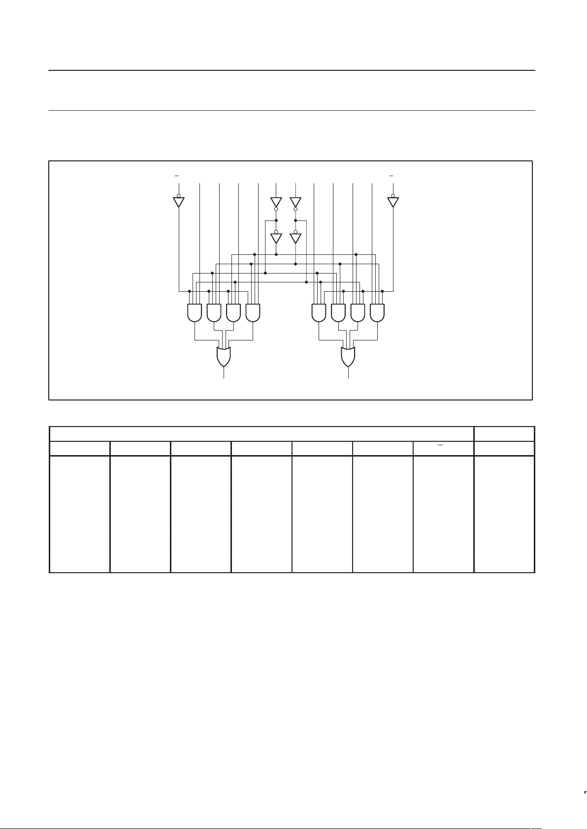
LOGIC DIAGRAM
7
Ya Yb
9
1 65432141011121315
V
CC
= Pin 16
GND = Pin 8
E
a EbI0a I1a I2a I3a S1 S2 I0b I0b I2b I3b
SF00149A
FUNCTION TABLE
INPUTS OUTPUT
S0 S1 I0n I1n I2n I3n En Yn
L L L X X X L L
L L H X X X L H
H L X L X X L L
H L X H X X L H
L H X X L X L L
L H X X H X L H
H H X X X L L L
H H X X X H L H
H = High voltage level
L = Low voltage level
X = Don’t care
 Loading...