

Philips N74ALS151D Datasheet
74ALS151
8-input multiplexer
Product specification 1991 Feb 08
INTEGRATED CIRCUITS
IC05 Data Handbook
Philips Semiconductors Product specification
74ALS1518-input multiplexer
2
1991 Feb 08 853–1022 01670
FEA TURES
•8-to-1 multiplexing
•On chip decoding
•Multi-function capability
•Complementary outputs
•See 74ALS251 for 3-State version
DESCRIPTION
The 74ALS151 is a logic implementation of a single 8-position
switch with the switch position controlled by the state of three select
(S0, S1, S2) inputs. True (Y) and complementary (Y
) outputs are
both provided.
The enable (E
) is active-Low. When E is High, Y output is Low and
the Y
output is High regardless of all other inputs.
TYPE
TYPICAL
PROPAGATION DELAY
TYPICAL
SUPPLY CURRENT
(TOTAL)
74ALS151 8.0ns 8.0mA
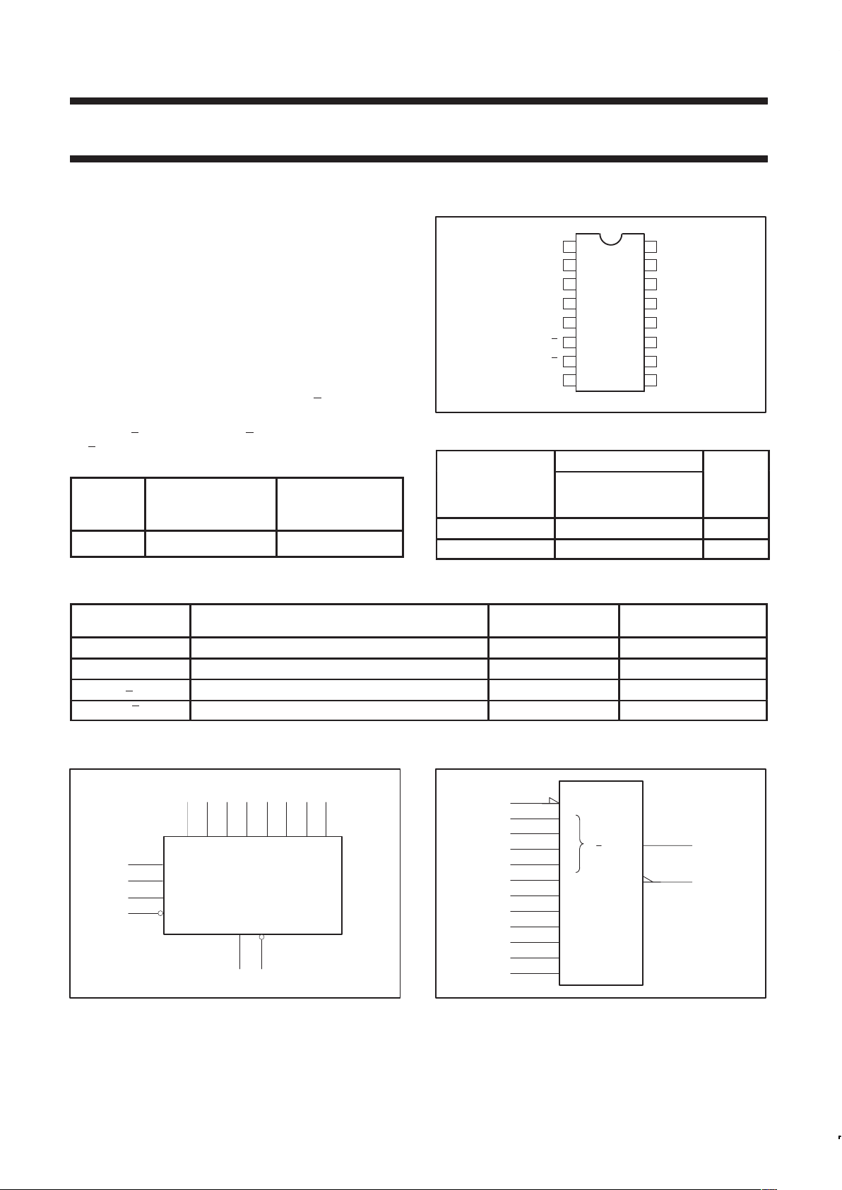
PIN CONFIGURATION
16
15
14
13
12
11
107
6
5
4
3
2
1
E
V
CC
I7
S0
S1
I6
I4
I5
I3
I2
Y
I1
I0
Y
98GND S2
SF00742
ORDERING INFORMA TION
ORDER CODE
DESCRIPTION COMMERCIAL RANGE
V
CC
= 5V ±10%,
T
amb
= 0°C to +70°C
DRAWING
NUMBER
16-pin plastic DIP 74ALS151N SOT38-4
16-pin plastic SO 74ALS151D SOT109-1
INPUT AND OUTPUT LOADING AND FAN-OUT TABLE
PINS DESCRIPTION
74ALS (U.L.)
HIGH/LOW
LOAD VALUE
HIGH/LOW
I0 – I7 Data inputs 1.0/1.0 20µA/0.1mA
S0 – S2 Select inputs 1.0/1.0 20µA/0.1mA
E Enable input (active-Low) 1.0/1.0 20µA/0.1mA
Y, Y Data outputs 130/240 2.6mA/24mA
NOTE: One (1.0) ALS unit load is defined as: 20µA in the High state and 0.1mA in the Low state.
LOGIC SYMBOL
123
V
CC
= Pin 16
GND = Pin 8
SF00743
65
11
10
9
S0
S1
S2
7
4 12131415
E
YY
I0 I1 I2 I3 I4 I5 I6 I7
IEC/IEEE SYMBOL
SF00744
MUX
7
11
3
2
1
5
6
0
G
0
7
10
2
EN
9
4
14
13
12
15
Philips Semiconductors Product specification
74ALS1518-input multiplexer
1991 Feb 08
3
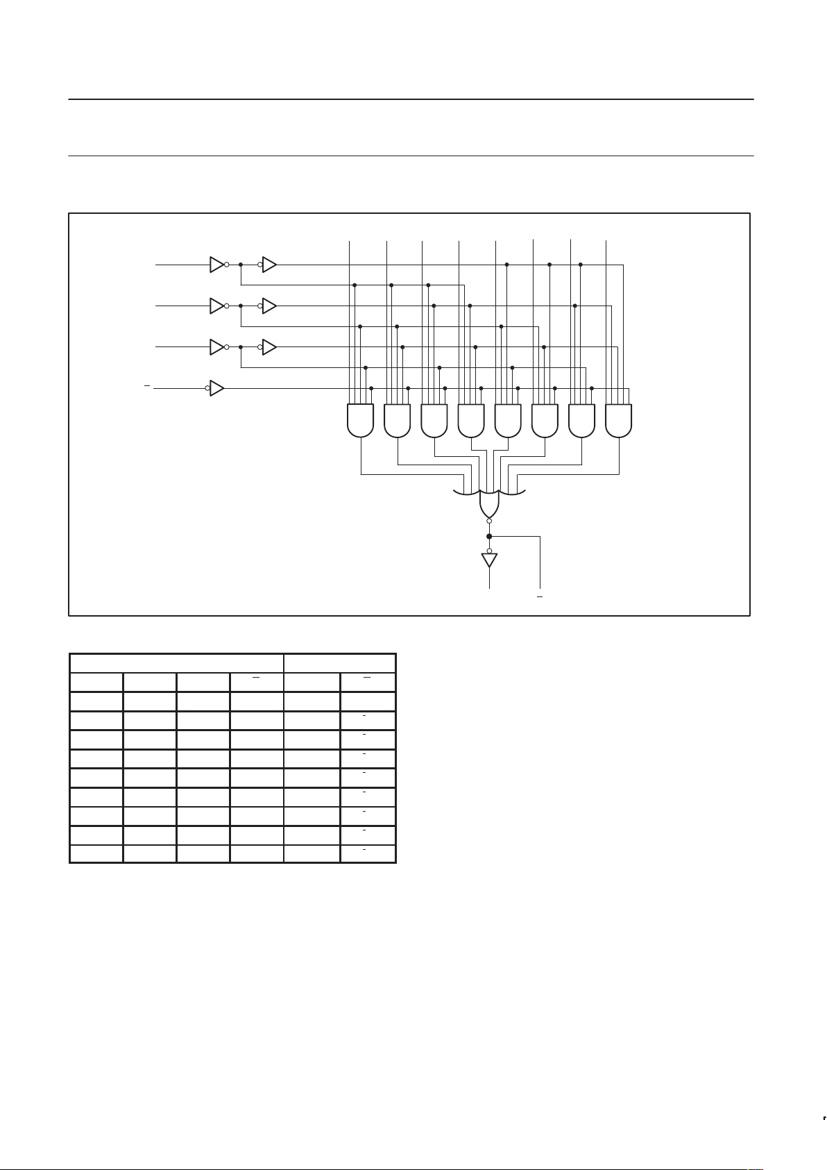
LOGIC DIAGRAM
9
10
11
V
CC
= Pin 16
GND = Pin 8
SF00741
YY
56
4 3 2 1 15 14 13 12
I0 I1 I2 I3 I4 I5 I6 I7
7
E
S0
S1
S2
FUNCTION TABLE
INPUTS OUTPUTS
S2 S1 S0 E Y Y
X X X H L H
L L L L I0 I0
L L H L I1 I1
L H L L I2 I2
L H H L I3 I3
H L L L I4 I4
H L H L I5 I5
H H L L I6 I6
H H H L I7 I7
H = High voltage level
L = Low voltage level
X = Don’t care
 Loading...